
1.0 V-0.18 µm CMOS Tunable Low Pass Filters with 73 dB DR for On-Chip Sensing Acquisition Systems


Abstract
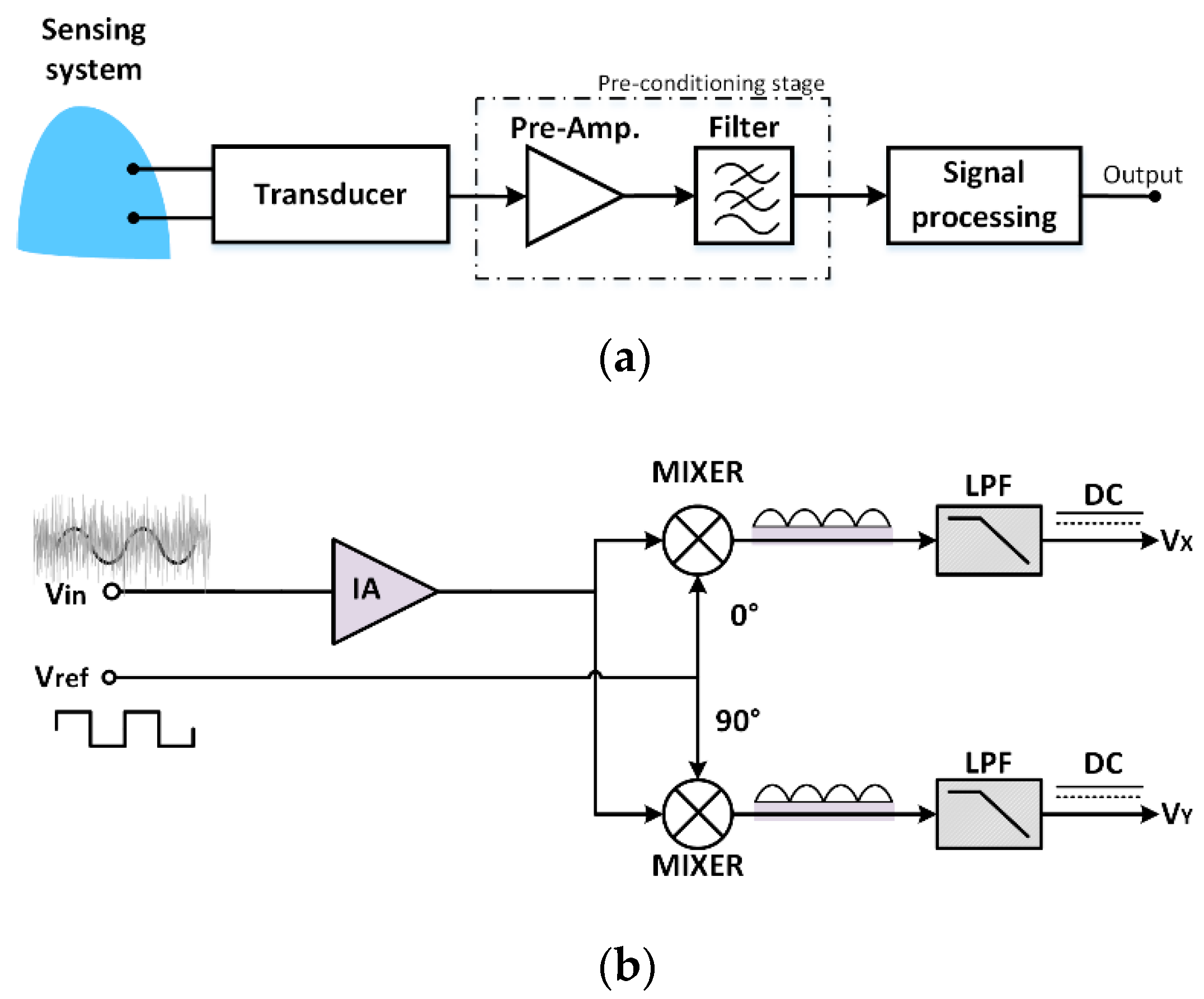
1. Introduction
2. Low Pass Filter Proposed Topology
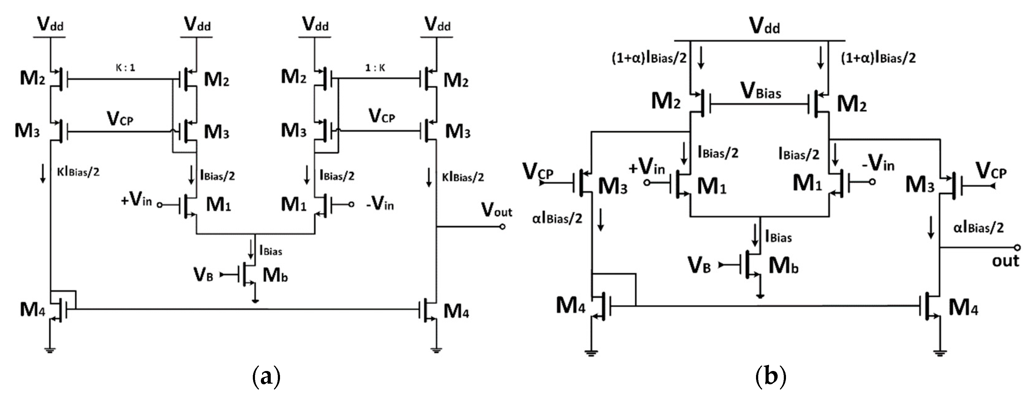
2.1. Core OTAs
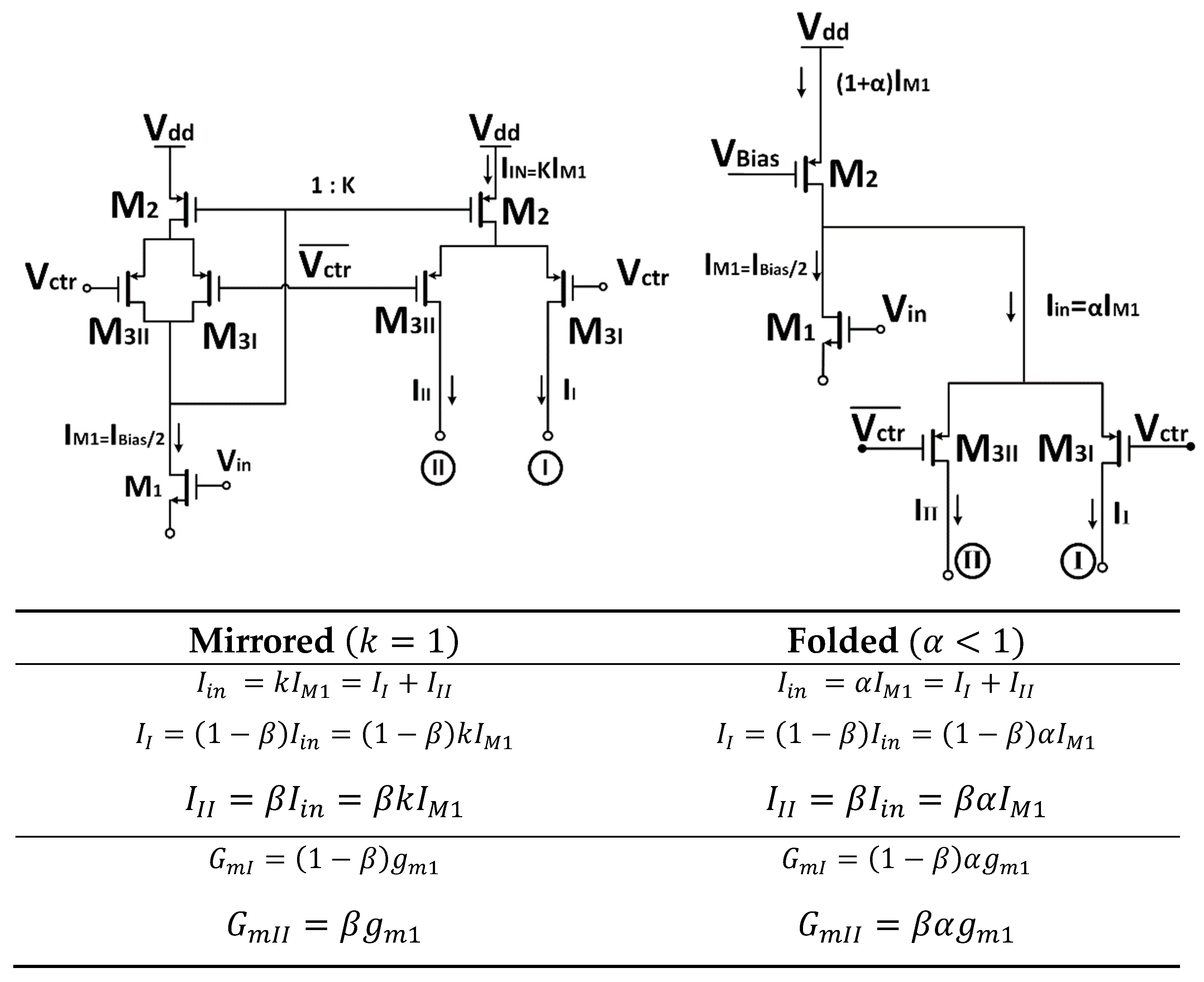
2.2. Gm Tuning Technique
2.3. Integrated Low Pass Filter
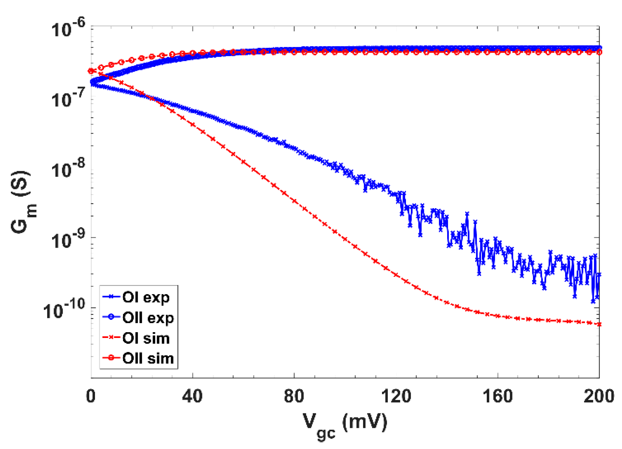
2.3.1. Mirrored-OTA Based Low Pass Filter
2.3.2. Folded-OTA Based Low Pass Filter
3. Experimental Characterization
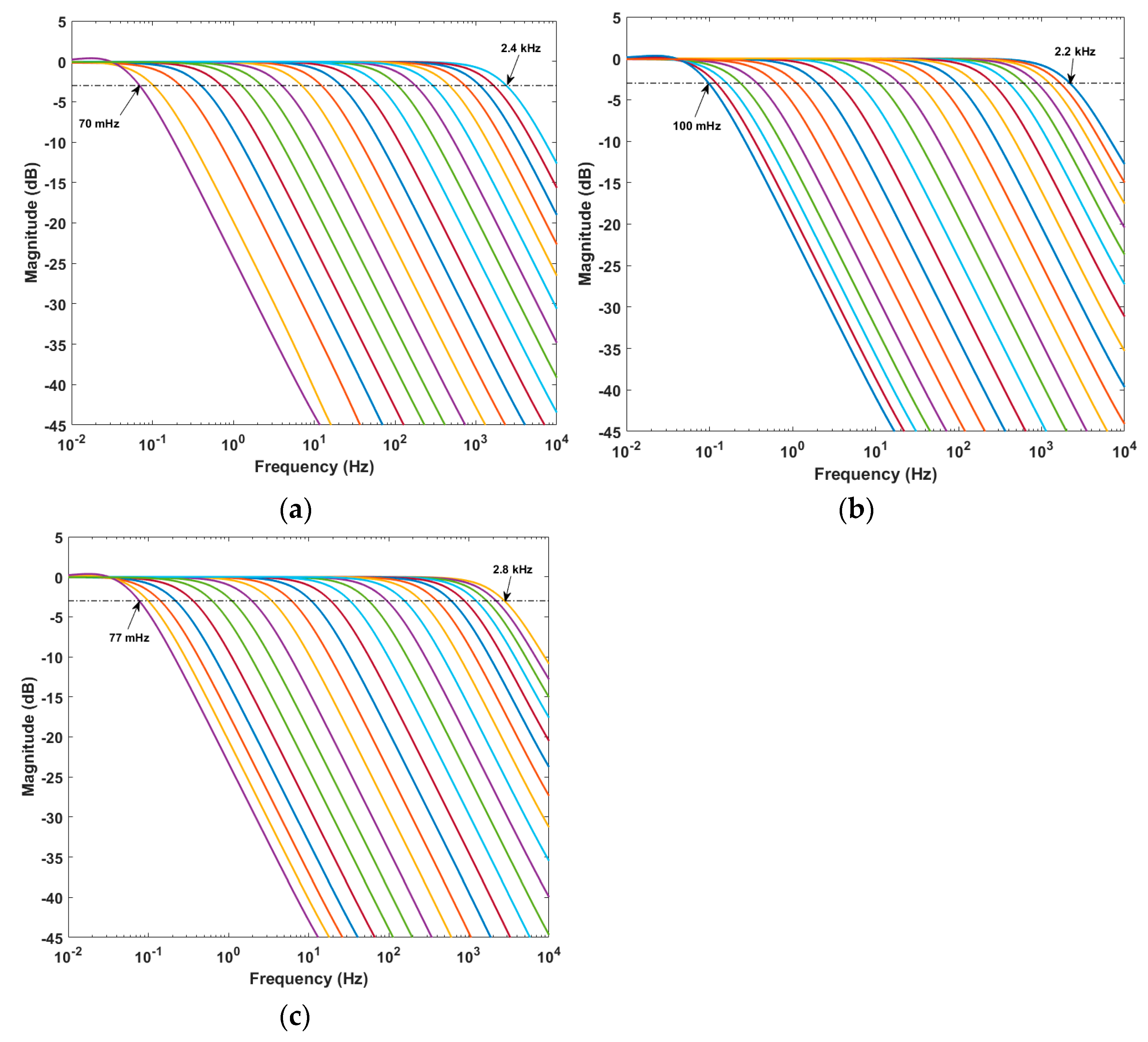
3.1. Cutoff Frequency Tunable Range
3.2. Input Common Mode Range (ICMR)
3.3. Linearity (@THD ≤ 1%)
3.4. Dynamic Range (DR)
3.5. Figure of Merit (FoM)
4. Conclusions
Author Contributions
Funding
Data Availability Statement
Acknowledgments
Conflicts of Interest
References
- Lee, S.; Wang, C.; Chu, Y. Low-Voltage OTA–C Filter With an Area- and Power-Efficient OTA for Biosignal Sensor Ap-plications. IEEE TBIOCAS 2019, 13, 56–67. [Google Scholar]
- Sawigun, C.; Thanapitak, S. A 0.9-nW, 101-Hz, and 46.3-µVrmsIRN Low-Pass Filter for ECG Acquisition Using FVF Bi-quads. IEEE TVLSI Syst. 2018, 26, 2290–2298. [Google Scholar] [CrossRef]
- Chang, S.-I.; Park, S.-Y.; Yoon, E. Low-Power Low-Noise Pseudo-Open-Loop Preamplifier for Neural Interfaces. IEEE Sens. J. 2017, 17, 4843–4852. [Google Scholar] [CrossRef]
- Xu, J.; Konijnenburg, M.; Ha, H.; Van Wegberg, R.; Lukita, B.; Asl, S.Z.; Van Hoof, C.; Van Helleputte, N. A 36μW reconfigurable analog front-end IC for multimodal vital signs monitoring. In Proceedings of the 2017 Symposium on VLSI Circuits, Kyoto, Japan, 5–8 June 2017; p. 170. [Google Scholar]
- Giaconia, G.C.; Greco, G.; Mistretta, L.; Rizzo, R. Exploring FPGA-Based Lock-In Techniques for Brain Monitoring Applications. Electronics 2017, 6, 18. [Google Scholar] [CrossRef]
- Sanchez-Gonzalez, A.; Medrano, N.; Calvo, B.; Martinez, P.A. A Multichannel FRA-Based Impedance Spectrometry Analyzer Based on a Low-Cost Multicore Microcontroller. Electronics 2019, 8, 38. [Google Scholar] [CrossRef]
- Chiriacò, M.S.; Parlangeli, I.; Sirsi, F.; Poltronieri, P.; Primiceri, E. Impedance Sensing Platform for Detection of the Food Pathogen Listeria monocytogenes. Electronics 2018, 7, 347. [Google Scholar] [CrossRef]
- Shaikh, M.O.; Srikanth, B.; Zhu, P.-Y.; Chuang, C.-H. Impedimetric Immunosensor Utilizing Polyaniline/Gold Nanocomposite-Modified Screen-Printed Electrodes for Early Detection of Chronic Kidney Disease. Sensors 2019, 19, 3990. [Google Scholar] [CrossRef]
- Li, H.; Liu, X.; Li, L.; Mu, X.; Genov, R.; Mason, A.J. CMOS Electrochemical Instrumentation for Biosensor Microsystems: A Review. Sensors 2016, 17, 74. [Google Scholar] [CrossRef]
- Ortiz-Aguayo, D.; Del Valle, M. Label-Free Aptasensor for Lysozyme Detection Using Electrochemical Impedance Spectroscopy. Sensors 2018, 18, 354. [Google Scholar] [CrossRef] [PubMed]
- Maya, P.; Calvo, B.; Sanz-Pascual, M.T.; Osorio, J. Low Cost Autonomous Lock-In Amplifier for Resistance/Capacitance Sensor Measurements. Electronics 2019, 8, 1413. [Google Scholar] [CrossRef]
- Maya-Hernandez, P.M.; Calvo-Lopez, B.; Sanz-Pascual, M.T. Ultralow-Power Synchronous Demodulation for Low-Level Sensor Signal Detection. IEEE Trans. Instrum. Meas. 2018, 68, 3514–3523. [Google Scholar] [CrossRef]
- De Marcellis, A.; Ferri, G.; D’Amico, A. One-Decade Frequency Range, In-Phase Auto-Aligned 1.8 V 2 mW Fully Analog CMOS Integrated Lock-In Amplifier for Small/Noisy Signal Detection. IEEE Sens. J. 2016, 16, 5690–5701. [Google Scholar] [CrossRef]
- Manickam, A.; Chevalier, A.; McDermott, M.; Ellington, A.D.; Hassibi., A. CMOS Electrochemical Impedance Spectros-copy (EIS) Biosensor Array. IEEE TBIOCAS 2010, 4, 379–390. [Google Scholar]
- Webster, J.G. Medical Instrumentation: Application and Design, 4th ed.; Wiley: New York, NY, USA, 1998. [Google Scholar]
- Liu, X.; Jiang, H. Construction and Potential Applications of Biosensors for Proteins in Clinical Laboratory Diagnosis. Sensors 2017, 17, 2805. [Google Scholar] [CrossRef] [PubMed]
- Wu, J.; Dong, M.; Santos, S.; Rigatto, C.; Liu, Y.; Lin, F. Lab-on-a-Chip Platforms for Detection of Cardiovascular Disease and Cancer Biomarkers. Sensors 2017, 17, 2934. [Google Scholar] [CrossRef] [PubMed]
- Arnaud, A.; Fiorelli, R.; Galup-Montoro, C. Nanowatt, Sub-nS OTAs, With Sub-10-mV Input Offset, Using Series-Parallel Current Mirrors. IEEE J. Solid-State Circuits 2006, 41, 2009–2018. [Google Scholar] [CrossRef]
- Solis-Bustos, S.; Silva-Martinez, J.; Maloberti, F.; Sanchez-Sinencio, E. A 60-dB dynamic-range CMOS sixth-order 2.4-Hz low-pass filter for medical applications. IEEE Trans. Circuits Syst. II Express Briefs 2000, 47, 1391–1398. [Google Scholar] [CrossRef]
- Rieger, R.; Demosthenous, A.; Taylor, J. A 230-nW 10-s time constant CMOS integrator for an adaptive nerve signal amplifier. IEEE J. Solid-State Circuits 2004, 39, 1968–1975. [Google Scholar] [CrossRef]
- Elfaramawy, T.; Rezaei, M.; Morissette, M.; Lellouche, F.; Gosselin, B. Ultra-low distortion linearized pseudo-RC low-pass filter. In Proceedings of the 2016 IEEE International Conference on Electronics, Circuits and Systems (ICECS), Monte Carlo, Monaco, 11–14 December 2016; pp. 221–224. [Google Scholar]
- Zhang, T.; Pui-In, M.; Mang-I, V.; Peng-Un, M.; Man-Kay, L.; Sio-Hang, P.; Fen, W.; Martins, R.P. 15-nW Biopotential LPFs in 0.35-µm CMOS Using Subthreshold-Source-Follower Biquads With and Without Gain Compensation. IEEE TBIOCAS 2013, 7, 690–702. [Google Scholar]
- M.K., J.R.; Polineni, S.; Tonse, L. 91dB Dynamic Range 9.5nW Low Pass Filter for Bio-Medical Applications. In Proceedings of the 2018 IEEE Computer Society Annual Symposium on VLSI (ISVLSI), Hong Kong, China, 8–11 July 2018; pp. 453–457. [Google Scholar]
- Peng, S.-Y.; Lee, Y.-H.; Wang, T.-Y.; Huang, H.-C.; Lai, M.-R.; Lee, C.-H.; Liu, L.-H. A Power-Efficient Reconfigurable OTA-C Filter for Low-Frequency Biomedical Applications. IEEE Trans. Circuits Syst. I Regul. Pap. 2017, 65, 543–555. [Google Scholar] [CrossRef]
- Lee, S.-Y.; Cheng, C.-J. Systematic Design and Modeling of a OTA-C Filter for Portable ECG Detection. IEEE Trans. Biomed. Circuits Syst. 2009, 3, 53–64. [Google Scholar] [CrossRef] [PubMed]
- Gosselin, B.; Sawan, M.; Kerherve, E. Linear-Phase Delay Filters for Ultra-Low-Power Signal Processing in Neural Re-cording Implants. IEEE TBIOCAS 2010, 4, 171–180. [Google Scholar]
- Sun, C.; Lee, S. A Fifth-Order Butterworth OTA-C LPF With Multiple-Output Differential-Input OTA for ECG Applica-tions. IEEE TCASII Express Briefs 2018, 65, 421–425. [Google Scholar]
- Valente, V.; Demosthenous, A. Wideband Fully-Programmable Dual-Mode CMOS Analogue Front-End for Electrical Impedance Spectroscopy. Sensors 2016, 16, 1159. [Google Scholar] [CrossRef]
- Badets, F.; Coutard, J.-G.; Russo, P.; Dina, E.; Glière, A.; Nicoletti, S. A 1.3 mW, 12-bit Lock-In Amplifier Based Readout Cir-cuit Dedicated to Photo-Acoustic Gas Sensing. In Proceedings of the IEEE Sensors 2016, Orlando, FL, USA, 30 October–3 November 2016; pp. 1–3. [Google Scholar]
- Pérez-Bailón, J.; Calvo, B.; Medrano, N. A CMOS Low Pass Filter for SoC Lock-in-Based Measurement Devices. Sensors 2019, 19, 5173. [Google Scholar] [CrossRef] [PubMed]
- Pérez-Bailón, J.; Márquez, A.; Calvo, B.; Medrano, N.; Sanz-Pascual, M.T. A 1V–1.75μW Gm-C low pass filter for bio-sensing applications. In Proceedings of the IEEE 9th Latin American Symposium on Circuits & Systems (LASCAS), Puerto Vallarta, Mexico, 25–28 February 2018; pp. 1–4. [Google Scholar]
- Ramírez-Angulo, J.; Sudha Gariemlla, S.R.; Lopez-Martin, A. New Gain Programmable Current Mirrors Based on Current Steering. In Proceedings of the IEEE International Midwest Symposium on Circuits and Systems (MWSCAS), San Juan, PR, USA, 6–9 August 2006. [Google Scholar]
- Sawigun, C.; Serdijn, W.A. A modular transconductance reduction technique for very low-frequency Gm-C filters. In Proceedings of the 2012 IEEE International Symposium on Circuits and Systems, Seoul, Korea, 20–23 May 2012; pp. 1183–1186. [Google Scholar]
- Tajalli, A.; Leblebici, Y. Low-Power and Widely Tunable Linearized Biquadratic Low-Pass Transconductor-C Filter. IEEE Trans. Circuits Syst. II Express Briefs 2011, 58, 159–163. [Google Scholar] [CrossRef]
- Ferreira, L.H.C.; Pimenta, T.C.; Moreno, R.L. An Ultra-Low-Voltage Ultra-Low-Power Weak Inversion Composite MOS Transistor: Concept and Applications. IEICE Trans. Electron. 2008, E91, 662–665. [Google Scholar] [CrossRef]
- Naik, S.; Bale, S.; Dessai, T.R.; Kamat, G.; M.H., V.; Vasantha, M. 0.5 V, 225 nW, 100 Hz Low pass filter in 0.18 µm CMOS process. In Proceedings of the 2015 IEEE International Advance Computing Conference (IACC), Banglore, India, 12–13 June 2015; pp. 590–593. [Google Scholar]


| Technique | Signal | Frequency Range |
|---|---|---|
| Biosignal front-end interface [1,15] | Blood flow | DC–20 |
| EMG | 10–200 | |
| ECG | 0.01–250 | |
| Phonocardiography | 5–2 k | |
| Nerve potential | DC–10 k | |
| Impedance Spectroscopy [9,16,17] | Gas detection, Molecular diagnosis, Cell evaluation | Sub-Hz–10 |
| Parameter | Filt-1 | Filt-2 | Filt-3 | Filt-2 | Filt-3 | [36] ‘15 | [21] ‘16(c) | [23] ‘18 | [24] ‘18 | [1] ‘19 |
|---|---|---|---|---|---|---|---|---|---|---|
| Results | Exp. | Exp. | Exp. | Exp. | Exp. | Lay. | Lay. | Sim. | Exp. | Sim. |
| Tech. (µm) | 0.18 | 0.18 | 0.18 | 0.18 | 0.18 | 0.18 | 0.18 | 0.18 | 0.35 | 0.18 |
| Fully-integrated | Yes | Yes | Yes | Yes | Yes | No | Yes | Yes | Yes | Yes |
| Vsupply (V) | 1.0 | 1.0 | 1.0 | 1.0 | 1.0 | 0.5 | 1.8 | 1.8 | 1.8 | 1 |
| Order | 1 | 1 | 1 | 1 | 1 | 2 | 2 | 2 | 2 | 5 |
| Gain offset (dB) | <0.5 | <0.5 | <0.5 | <0.5 | <0.5 | −0.5 | NA | −3.2; −7.2 | NA | −7 |
| Area (mm2) | 0.0137 | 0.0135 | 0.0136 | 0.0135 | 0.0136 | NA | 0.062 | NA | 0.12 | 0.24 |
| T range (°C) | −40–100 | −40–100 | −40–100 | −40–100 | −40–100 | NA | NA | NA | NA | 0–80 |
| IBias (nA) | 500 | 100 | 100 | 500 | 500 | 37.5 | NA | 1 | 14.9–182.3 | NA |
| Power (nW) | 1750 | 180 | 180 | 960 | 960 | 250 | 2.33*105 | 9.5 | 107.2–1310 | 41 |
| Tunable | Yes | Yes | Yes | Yes | Yes | No | Yes | Yes | Yes | No |
| fc (Hz) | 82.5 m–1.179 k | 109 m–152 | 104 m–141 | 94 m–1.475 k | 129 m–1.757 k | 100 | 34–20 k | 4–100 | 2 k–20 k | 250 |
| ICMR (V) | 0.4–0.97; 0.35–0.97(a) | 0.2–0.74; 0.15–0.76(a) | 0.15–0.85; 0.14–0.87(a) | 0.31–0.94; 0.35–0.95(a) | 0.19–0.94; 0.21–0.95(a) | NA | NA | NA | NA | NA |
| noise (µVrms) | 12.2; 15.5(a) | 9.48; 10.28(a) | 8.11; 8.81(a) | 7.75; 8.48(a) | 6.40; 7.33(a) | NA | 91.2 | 10.24(d) | 86.3–84.3 | 134 |
| Linearity (Vpp) | 0.167; 0.28(a) | 0.3; 0.236(a) | 0.248; 0.205(a) | 0.251; 0.222(a) | 0.246; 0.19(a) | 0.15 | NA | 1.03(d) | NA | NA |
| DR (dB) | 73.7; 76.1(a) | 81.0; 78.2(a) | 80.7; 78.3(a) | 81.2; 79.3(a) | 82.7; 79.2(a) | 74.62(b) | NA | 91(d) | 52.7; 54.6(e) | 61.2 |
| NP (FoM1) (10−9) | 1458 | 150 | 150 | 800 | 800 | 2500 | 46230 | 1.88 | 22.2; 271.6 | 34.2 |
| NA (FoM2) | 0.423 | 0.417 | 0.420 | 0.417 | 0.420 | NA | 1.914 | NA | 0.98 | 7.4 |
| FoM1 (10−12) | 301; 228(a) | 13.4; 18.5(a) | 13.4; 18.5(a) | 70; 87(a) | 59; 88(a) | 232 | NA | 0.0265 | 26; 253 | 5.96 |
| FoM2 (10−12) | 76.4; 580(a) | 3.34; 46.2(a) | 3.48; 46(a) | 17.4; 217(a) | 14.8; 221(a) | NA | NA | NA | 245; 23905 | 13.21 |
Publisher’s Note: MDPI stays neutral with regard to jurisdictional claims in published maps and institutional affiliations. |
© 2021 by the authors. Licensee MDPI, Basel, Switzerland. This article is an open access article distributed under the terms and conditions of the Creative Commons Attribution (CC BY) license (http://creativecommons.org/licenses/by/4.0/).
Share and Cite
Pérez-Bailón, J.; Calvo, B.; Medrano, N. 1.0 V-0.18 µm CMOS Tunable Low Pass Filters with 73 dB DR for On-Chip Sensing Acquisition Systems. Electronics 2021, 10, 563. https://doi.org/10.3390/electronics10050563
Pérez-Bailón J, Calvo B, Medrano N. 1.0 V-0.18 µm CMOS Tunable Low Pass Filters with 73 dB DR for On-Chip Sensing Acquisition Systems. Electronics. 2021; 10(5):563. https://doi.org/10.3390/electronics10050563
Chicago/Turabian StylePérez-Bailón, Jorge, Belén Calvo, and Nicolás Medrano. 2021. "1.0 V-0.18 µm CMOS Tunable Low Pass Filters with 73 dB DR for On-Chip Sensing Acquisition Systems" Electronics 10, no. 5: 563. https://doi.org/10.3390/electronics10050563
APA StylePérez-Bailón, J., Calvo, B., & Medrano, N. (2021). 1.0 V-0.18 µm CMOS Tunable Low Pass Filters with 73 dB DR for On-Chip Sensing Acquisition Systems. Electronics, 10(5), 563. https://doi.org/10.3390/electronics10050563