Article

Customizable Vector Acceleration in Extreme-Edge Computing: A RISC-V Software/Hardware Architecture Study on VGG-16 Implementation

Department of Information Engineering, Electronics and Telecommunications (DIET), Sapienza University of Rome, 00185 Rome, Italy
*
Author to whom correspondence should be addressed.
Electronics 2021, 10(4), 518; https://doi.org/10.3390/electronics10040518
Submission received: 26 January 2021 / Revised: 14 February 2021 / Accepted: 19 February 2021 / Published: 23 February 2021
(This article belongs to the Special Issue Advanced Embedded HW/SW Development)

Abstract

:
Computing in the cloud-edge continuum, as opposed to cloud computing, relies on high performance processing on the extreme edge of the Internet of Things (IoT) hierarchy. Hardware acceleration is a mandatory solution to achieve the performance requirements, yet it can be tightly tied to particular computation kernels, even within the same application. Vector-oriented hardware acceleration has gained renewed interest to support artificial intelligence (AI) applications like convolutional networks or classification algorithms. We present a comprehensive investigation of the performance and power efficiency achievable by configurable vector acceleration subsystems, obtaining evidence of both the high potential of the proposed microarchitecture and the advantage of hardware customization in total transparency to the software program.

1. Introduction

The cloud-edge continuum computing paradigm relies on the possibility of local processing in the edge of the IoT whenever it is convenient for reasons of energy efficiency, reliability, or data security. As a consequence, there is a gradual shift of artificial intelligence (AI) algorithm execution from the cloud down low power embedded IoT devices on the edge, to be used in real-time for example to take voice commands or extract image features, for biometric, security, or filtering purposes [1].
The resultant demand for very high processing speed on extreme edge computing devices turns into unprecedented design challenges, especially because of the usually limited energy budget. Therefore, the implementation of hardware acceleration on edge devices in the IoT hierarchy has become a major trend to reach the speed and energy efficiency requirements.
Vector computing acceleration was a major stream in high performance computing systems for decades and is gaining renewed interest in recent development in the supercomputing sector [2]. Yet, it is easy to note that the vector computing paradigm can also be applied to AI computing kernels that are run in embedded IoT devices on the edge. Nonetheless, the limited hardware budget usually available in edge devices makes it interesting to explore the possibility of configurable acceleration sub-systems to optimally exploit the available hardware resources according to the specific computation kernels being run during the application execution.
We implemented such exploration addressing the execution of the VGG-16 deep convolutional neural network inference, widely known for its image recognition performance as well as for its high computing power and storage demand. The VGG-16 execution is composed of consecutive layers having different computational characteristics. Therefore, it well represents a stress-test of the hardware micro-architecture with a time-variant workload profile. Our target micro-architecture is an open-source RISC-V [3] processor core supporting multi-threaded execution and featuring a highly customizable vector acceleration subsystem [4].
The contributions of this work to the reader interested in advanced embedded system design for IoT extreme-edge computing, are manifold:
  • We report the quantitative evidence of the trade-offs in vector co-processor design and configuration targeting simple edge-computing soft-cores;
  • We present details on the small custom RISC-V compliant instruction extension sufficient to support typical vector operations in a tiny soft-core;
  • We present a complete yet very simple library of intrinsic functions to support application development, and we discuss the full detail of source code exploiting the co-processor instructions in each VGG-16 layer execution;
  • We give insights into the open-source Klessydra processor core microarchitecture.
The rest of this article is organized as follows: Section 2 covers the related works on hardware acceleration for embedded computing on the IoT edge, including configurable solutions, Section 3 introduces the Klessydra T1 processor soft-core featuring configurable hardware acceleration subsystem. Section 4 describes the fundamental features of the VGG-16 application case and its implementation on Klessydra T1. Section 5 reports and discusses the results obtained for the different sub-parts of the chosen application cases, and Section 6 summarizes the outcomes of the work.

2. Related Works

Several previous works reported the design of hardware accelerated microcontroller cores implemented in edge-computing silicon chips. In [5], a RISC-V processor with DSP hardware support is presented, targeting near-threshold voltage operation. The Diet-SODA design implements a similar approach by running its DSP accelerator in near-threshold regime [6]. In [7,8,9] application specific accelerators are reported, based on highly parallel operation and minimized off-chip data movements for energy efficiency.
All of the above works focus on silicon implementation of units tailored to specific computations. As opposed to this view, the proposed hardware architecture study is independent of technology assumptions, such as the supply voltage, and addresses any physical implementation, particularly soft-cores on commercial FPGA devices, in the view of exploiting application-driven configurability. Regarding FPGA-based implementations, in [10] the authors present a cluster of RISC-V cores connected to a tightly-coupled scratchpad memory and a special purpose engine dedicated to convolutions only. Thanks to FPGA implementation, the convolution engine can be configured at synthesis time to optimize the execution of each convolutional layers, yet exhibiting a severe performance degradation when executing layers it was not built to optimize.
A recently published work [11] presents a SIMD configurable CNN coprocessor connected to a 32-bit RV32IM RISC-V processor. Compared to the pure SIMD Klessydra configuration, that uses 11678 LUTs and takes 824 clock cycles for a 4 × 4 matrix convolution, the work in [11] reports 12872 LUTs and 2070 clock cycles.
In [12] the authors present a coprocessor soft-core at the edge of IoT, designed to be energy efficient in executing CNN as well as other machine learning algorithms. In particular, they explore the potential impact of data parallelism on the energy efficiency due the increased memory bandwidth. In our study, memory traffic as well as the memory static power consumption are taken into account in energy estimations.
The works in [13,14] present a pipelined CNN coprocessor capable of accelerating convolutions based on the extremely high parallelism in the coprocessor, yet limited to convolutional computation kernels.
In [15] the authors present different coprocessor configurations integrated with a parallel cluster of RISC-V cores and evaluated which of the configurations is the fastest and most energy efficient. They introduce special co-processing cores dedicated to the standard instruction subset RV32M, without exploring more sophisticated co-processor operations.
In [16] the authors provide a DCNN accelerator for IoT. The accelerator itself is designed to work with 3 × 3 kernels, and being not configurable, in order to support larger kernels they use a technique called kernel decomposition, which in fact increases the waste in computational resources and decreases in the energy efficiency, similarly to the convolution engine in [10].
The coprocessor architecture proposed in this work is general purpose in nature, being based on vector operations, and can be tailored to support a given computation kernel in the most efficient way. Our work builds on the preliminary developments reported in [17,18] and complements the analysis presented in [4].
The standard “V” vector extension of RISC-V—supported for example by SiFive products [19] and by the EPAC accelerator within the European Processor Initiative project [2] is a large and complex instruction set extension, to cover applications ranging from embedded systems to HPC, which goes far beyond the scope of the lightweight Klessydra soft-core vector extension. Additionally, the standard “V” extension adopts a vector processing scheme based on a Vector Register File, while we explicitly chose to use generic Scratchpad Memories (SPMs) as local storage for more flexibility, at the price of losing compliance with any standard ISA extension. Rather than identifying vectors with a vector number chosen among 32 vector registers, we use pointers within the SPM address space to address vectors or portions of vectors. Additionally, as the number of SPMs available to the programmer in the microarchitecture is configurable.
The Ara processor [20], as well as the Xuantie-910 processor [21] and the dual core presented in [22], are all silicon ASIC implementations (thus not configurable as a soft-core is) of micro-architectures, which are actually not compliant with the “V” standard extension, yet they are still based on fixed Vector Register Files. Additionally, the Xuantie-910 processor addresses high performance superscalar execution of general-purpose non-vectorizable code, which is out of the scope of the Klessydra architecture.
The processor reported in [23] adopts an interesting approach based on directly converting ARM SVE vectorized code into a non-standard vector RISC-V extension, thus it is explicitly based on the same operation and storage scheme of ARM SVE. Klessydra diverges from this approach, favoring a broader exploration through configurability. The processor presented in [24] is a soft-core as Klessydra is, but it is again based on a Vector Register File rather than on a configurable SPM-based acceleration.

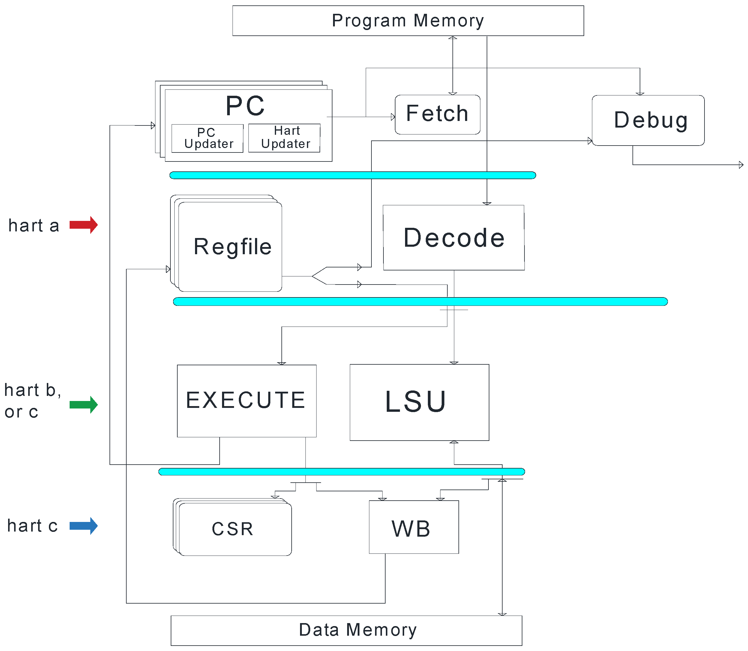
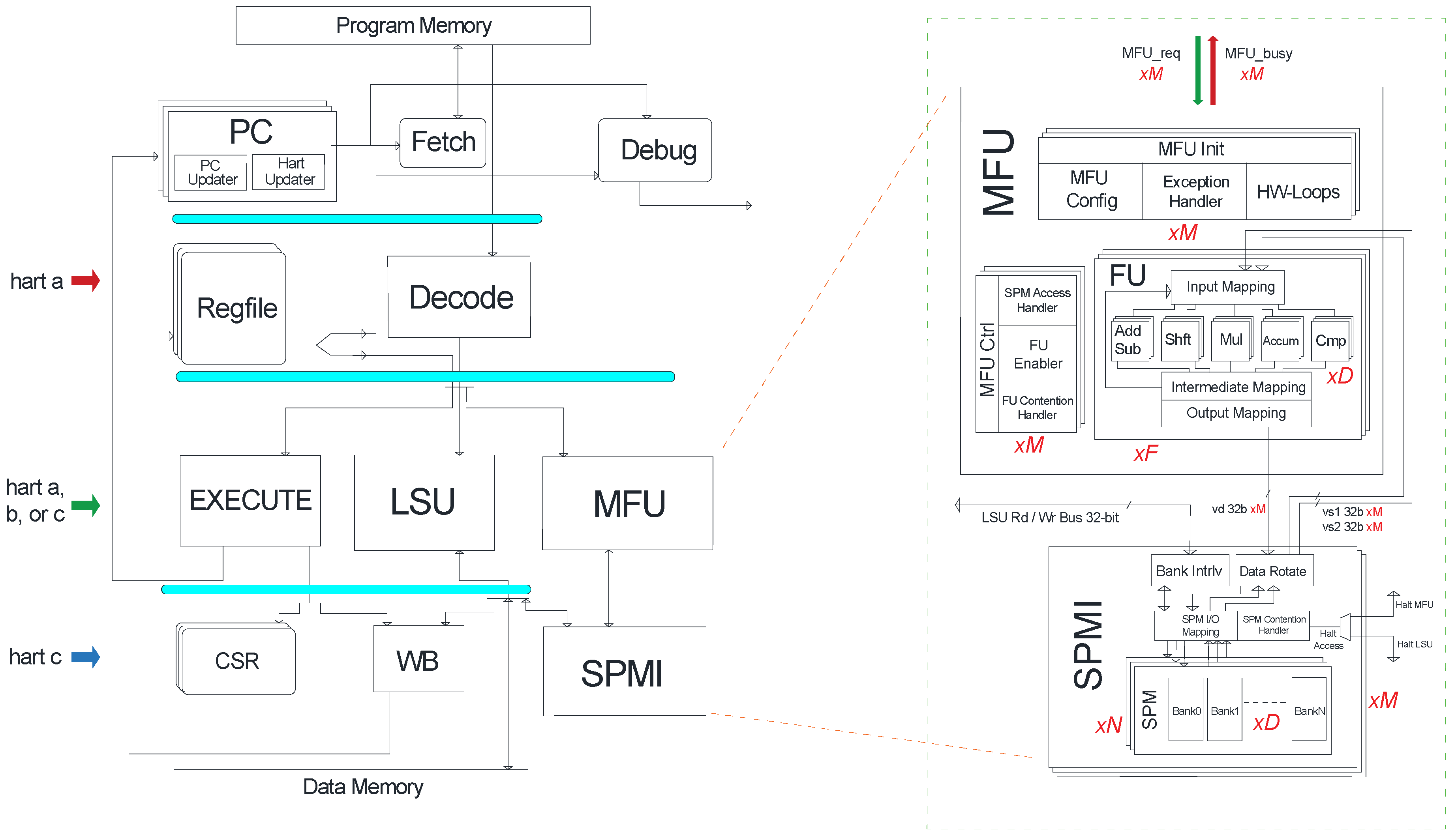
3. The Klessydra T1 Customizable Architecture

3.1. Hardware Microarchitecture

Klessydra is a family of open-source, RISC-V compliant and PULPino [25] compatible cores, which includes basic processors (T0 sub-family), hardware accelerated processors (T1 sub-family), and fault-tolerant processors (F0 sub-family) [26]. A characteristic feature of all Klessydra cores is the hardware support for interleaved multi-threading on a single core [27]. The RTL code and manuals of the Klessydra family are available in the Supplementary Materials.
The hardware accelerated T1 cores are an extension of the basic T0 core, that is sketched in Figure 1.
The T0 microarchitecture resembles a classic four-stage RISC pipeline, except for having multiple Program Counters to support multi-threading, and replicated register files and Control/Status Registers. Differently from a multi-core implementation, an interleaved multi-threading single core shares all the combinational logic constituting the instruction processing pipeline among the hardware threads (“harts” [3]), by interleaving threads in time, while maintaining separate PCs and registers to keep the state of each thread.
In each clock cycle a different Program Counter is used for instruction fetching, on a rotation basis. As a result, instructions belonging to different threads of execution are interleaved in the core pipeline, so that it is never possible that any two instructions in the pipeline manifest any register, structural or branch dependency. By fetching an instruction from a new thread in each clock cycle, pipeline hazards are eliminated, while if the same thread run for several clock cycles, its own data hazard or branching hazard would impose introducing dependency-check logic and pipeline stalling. The only dependency in the instruction pipeline can occur between two threads on explicit shared memory access, which is responsibility of the programmer.
The supported number of interleaved threads is a parameter of the synthesizable RTL code of the core.
The T1 microarchitecture (Figure 2) is derived from the T0 by adding the Vector Co-processing Unit (VCU), being internally comprised of Multi-Purpose Functional Units (MFU) and Scratch-Pad Memory Interface (SPMI).
At the instruction level, the T1 architecture supports the parallel execution of instructions of different types, belonging to the same hart. In fact, the LSU works in parallel with the other units when executing memory store instructions, that cannot cause a write-back conflict on the register file. The MFU is allowed to read operands from the register file but can only write its results to local scratchpad memories (SPMs), thus keeping the SPMs and the Registerfile decoupled and allowing parallel execution between instructions writing to each of these memories simultaneously. Scalar instructions of a hart are processed by the “Execution” unit and operate on data in the Register File, while vector instructions are processed by the VCU and operate on data in the SPMs. Data transfers to/from the data memory from/to the SPMs are managed by the LSU via dedicated instructions.
The MFUs execute vector arithmetic instructions, whose latency is proportional to the vector length. In an in-order interleaved-multi-threading pipeline, a hart requesting access to the busy MFUs may result in stalling the whole pipeline, stalling other harts that may not need to access the MFU. To circumvent this, in the T1 architecture, the waiting hart executes a self-referencing jump so that the PC for that hart does not advance until the MFU becomes free, avoiding unnecessary stalls of harts that are independent from the MFU being busy. Figure 3 demonstrates a cycle accurate diagram of the mechanism.
When deploying Klessydra T1 in a IoT edge device, one can configure the number of parallel lanes D in the MFU, the number of MFUs F, the SPM capacity, the number of independently accessible SPMs N in each SPMI, the number of SPMIs M, as well as the way the MFUs and SPMI are shared between the harts. Representative configurations are the following:
  • Thread-Shared coprocessor: All harts in the core share a single MFU/SPM subsystem. Harts in this scheme are required to execute an infinite jump when trying to access the MFU when its busy. In this approach, instruction level parallelism is limited to occur only between coprocessor instructions writing to the SPM and non-coprocessor instructions writing to the main memory or register file. To mitigate the delays on a hart executing an infinite jump, the coprocessor here may exploit pure data level parallelism (DLP) acceleration, by SIMD execution.
  • Thread-Dedicated coprocessor: Each hart is appointed a full MFU/SPM subsystem, eliminating inter-hart coprocessor contention and allowing inter-coprocessor parallel execution. Stalls can only happen if the next instruction of the same hart that is using the MFU requests an MFU operation. DLP by SIMD execution can still be exploited in this approach, but also thread level parallelism (TLP) by fully symmetric MIMD execution, allowing execution of multiple vector instructions in parallel.
  • Thread-Dedicated SPMIs with a Shared MFU: The harts here maintain a dedicated SPM address space, yet they share the functional units in the MFU. This scheme still allows inter-hart parallel execution of coprocessor instructions, provided they use different internal functional units (FU) of the MFU (e.g., adder, multiplier). Harts that request a busy internal unit in the MFU will be stalled, and their access will be serialized until the contended unit becomes free, while harts that request a free functional unit can work in parallel with the other active harts in the MFU. DLP by SIMD execution can still be exploited in this approach, but also TLP by heterogeneous MIMD execution.
Table 1 summarizes the design parameters and corresponding configurations, whose names will be used as references in reporting performance results.

3.2. Programming Paradigm

By default, a Klessydra core runs the maximum number of hardware threads (which is a synthesis parameter) allowed by the microarchitecture. The function Klessydra_get_coreID() can read the id number of the thread executing the function from the MHARTID CSR register, so this allows to distinguish threads and possibly have each thread to execute a different piece of program. Figure 4 shows a generic C program skeleton in which each of the three threads executes its own instruction flow. The functions sync_barrier_thread_registration() and sync_barrier() allow implementing a synchronization barrier by based on inter-thread software interrupts, to synchronize thread execution at certain points of the program.
Figure 5 gives a representation of the memory map assumed by the Klessydra T1 operation.
The SPM local storage is visible to the programmer as a specific address region in the memory map. The programmer can move data to/from any point of the SPM address space with no constraint except the total capacity of the SPMs, which in turn is a parameter of the microarchitecture design.
Inter-thread data transfers may happen via shared global static variables allocated in the main data memory or, in the case of a shared coprocessor configuration, via shared SPM address space. As in any multi-threading execution scheme, access to shared data must be accompanied by explicit thread synchronization, which is available in Klessydra by means of specific intrinsic functions implementing semaphore locks compliant with RISC-V atomic instructions, not in the scope of this work.
The custom instruction extension supported by the VCU and LSU is summarized in Table 2. The instructions supported by the coprocessor sub-system are exposed to the programmer in the form of very simple intrinsic functions, fully integrated in the RISC-V gcc compiler toolchain. The compiler does not have knowledge of the hardware configuration, so it only translates the intrinsic functions into the corresponding dedicated vector instructions, which are then executed by the hardware according to the chosen hardware configuration. The instructions implement vector operations working on the memory space mapped on the local SPMs. The vector length applied by MFU operations is encoded in a user accessible custom control/status register (CSR) named MVSIZE.

4. VGG-16 Implementation on Klessydra T1

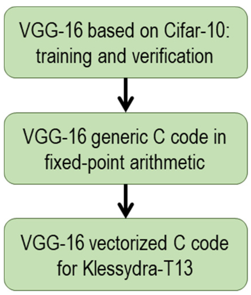
4.1. Implementation Workflow

VGG-16 is a deep Convolutional Neural Network (CNN) used in computer vision for classification and detection tasks, consisting of 13 convolutional layers, 5 maxpooling layers, 2 fully-connected layers and one output/softmax layer. The original VGG-16 can label a 224 × 224 pixel RGB image to one class out of 1000, using approximately 554 MB space for 32-bit floating-point weights and bias values.
In the view of a realistic IoT edge embedded scenario, we implemented a VGG-16 derivation based on the widely known CIFAR-10 dataset, targeting 10 classes and 32 × 32 pixel RGB images and requiring 135 MB for weights and bias values. Table 3 reports the breakdown of the inference algorithm layers constituting the Cifar-10 VGG-16. The layers 19 to 21 do not compute operations on matrices, rather they implement dot-product operations between vectors of different sizes, similarly, layer 22 implements a Softmax function on a vector of length 10.
Figure 6 illustrates the workflow to implement a Cifar-10 VGG-16 application on the Klessydra processor platform. Notably, since the target hardware platform supports fixed-point arithmetic, we based the implementation on fixed-point weights and data. We set the integer part to 11 bits and the fractional part to 21 bits, which leads an accuracy drop from 98.04% to 84.01% on the of output results of the inference. We remark that re-training the network, as well as further algorithmic optimizations, such as quantization and compression techniques, are not in the scope of the present work. The verification phase of the network in fixed point arithmetic was done via MATLAB (The MathWorks, Natick, MA, USA) Deep Learning Toolbox. In order to be able to exploit the C language intrinsic functions of the Klessydra platform, the original MATLAB code for VGG-16 was ported to C code. This generic C code implementation was used as the basis for the subsequent vectorization to exploit the hardware co-processor, and it was also used to run the same algorithm on the reference platforms used for performance comparison. We verified that no additional loss of quality is introduced by the proposed hardware architecture, which produces an identical output to the C fixed-point version executed on a general purpose computer.

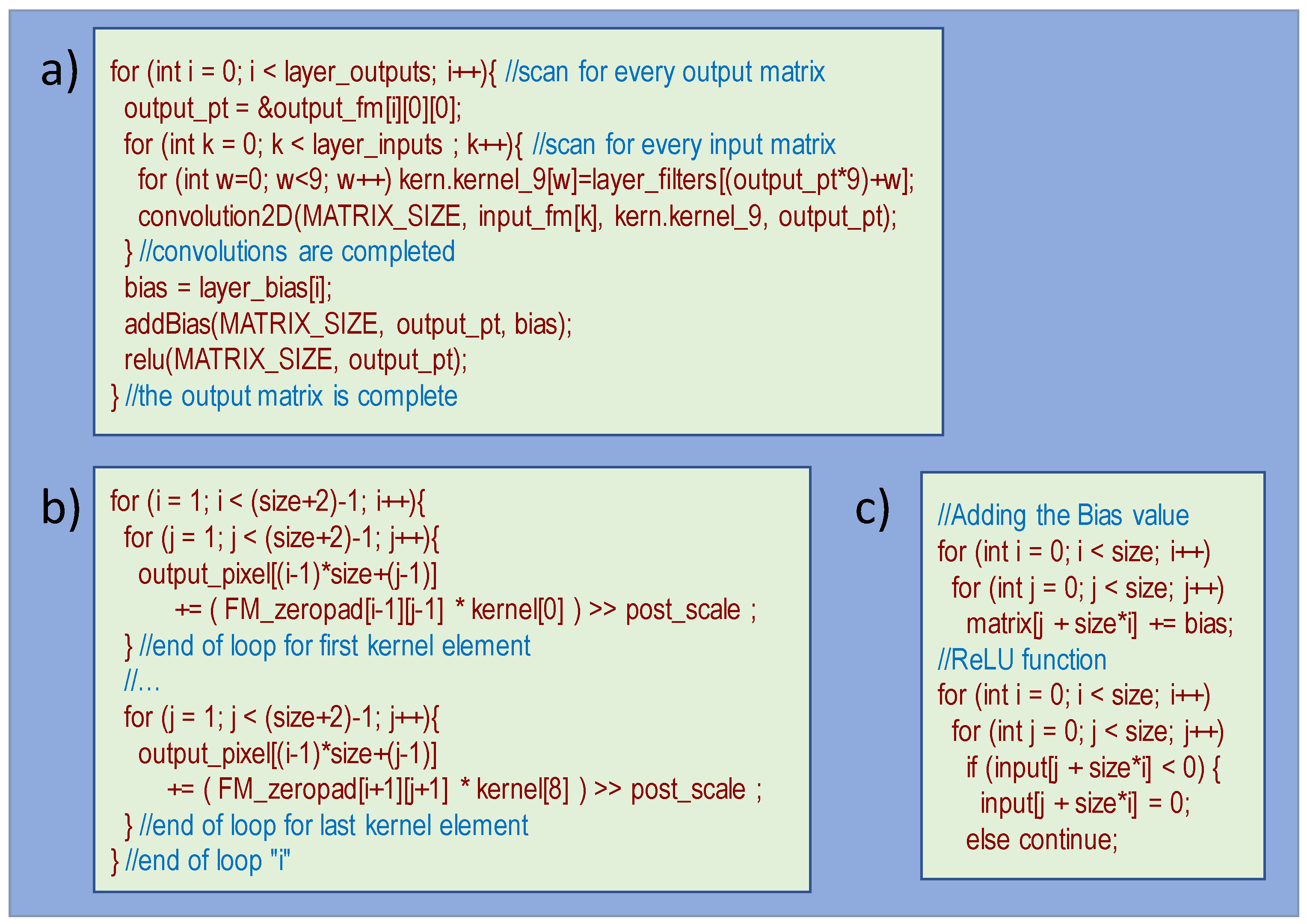
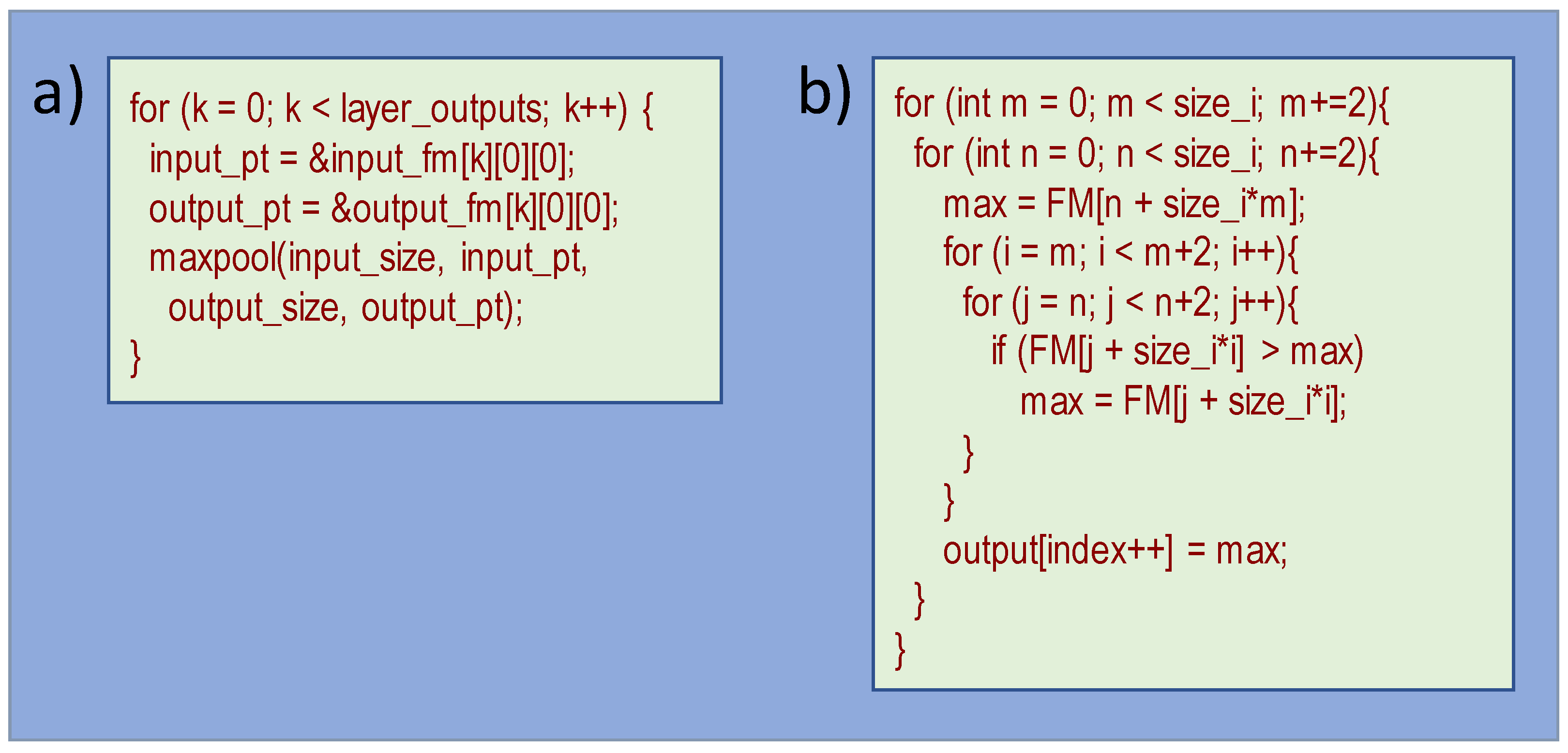
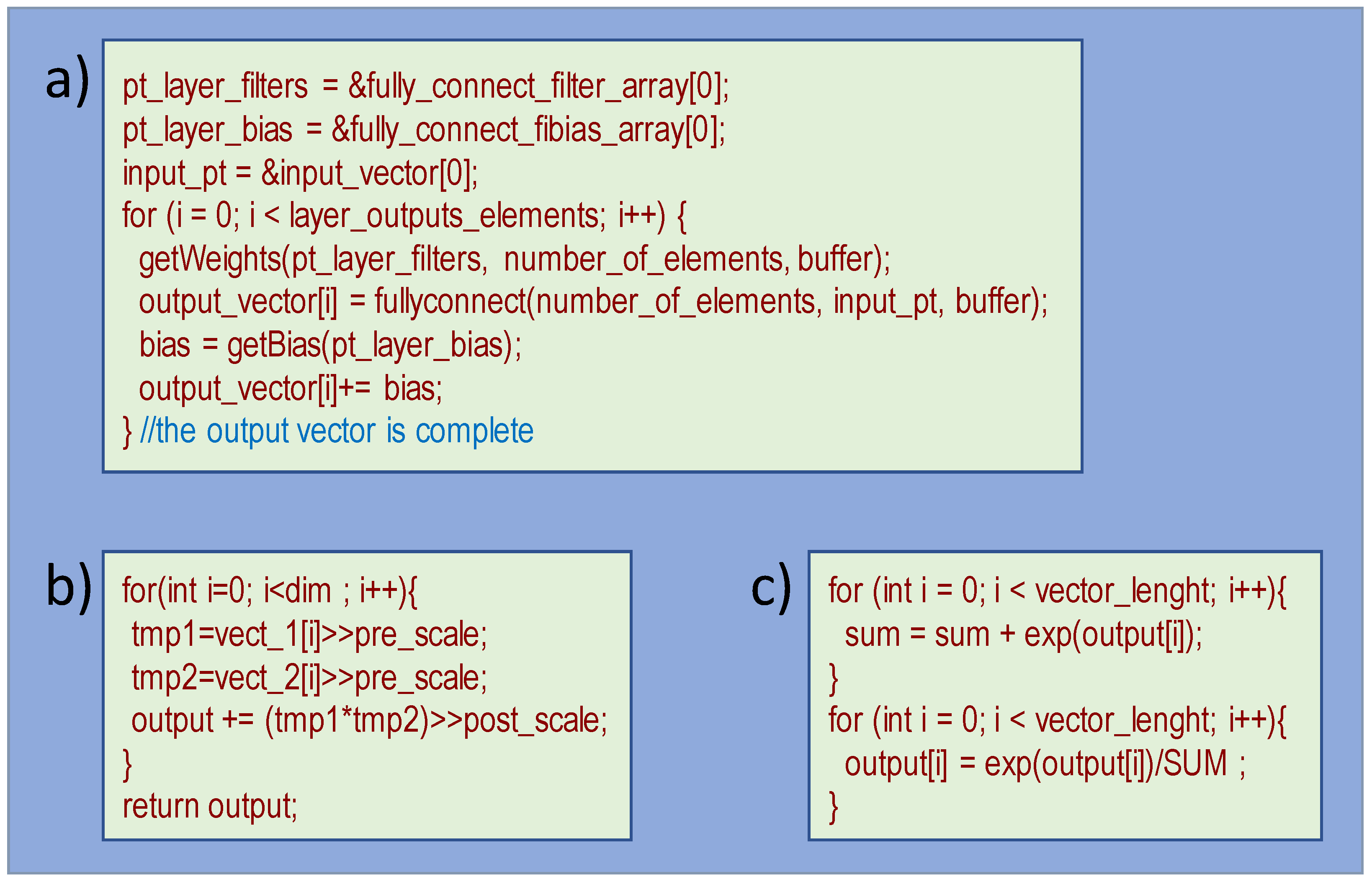
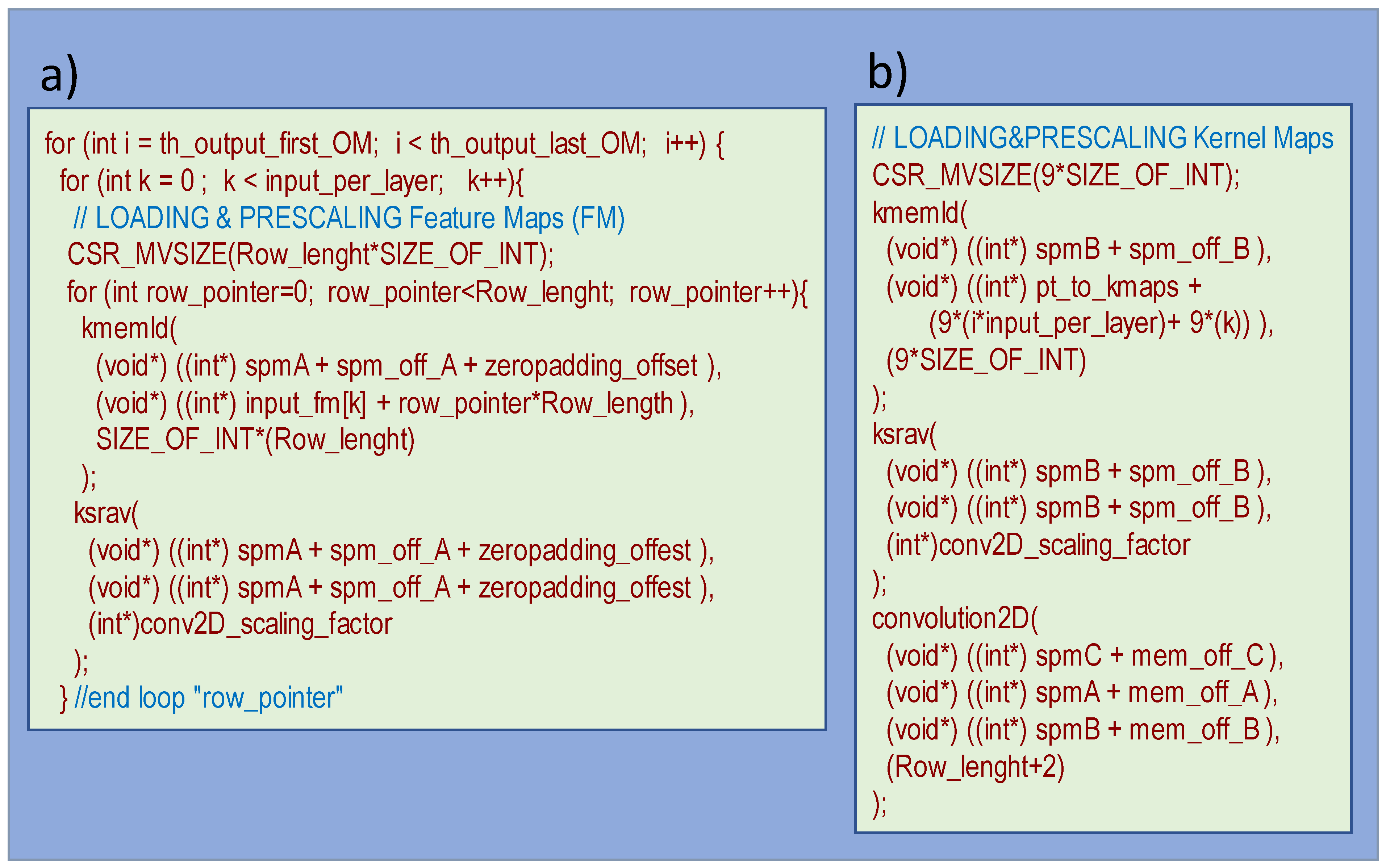
4.2. Generic Fixed-Point C Code Porting

The generic C code used for convolutional layers is reported in Figure 7. Image convolutions are implemented using the zero-padding technique: the feature map (FM) matrix is converted into a new matrix having two additional rows and columns of zeros on its borders, to avoid having filter elements without corresponding pixel values when the centroid element of the 3 × 3 kernel slides along the borders. As a general feature of the implementation, multiplications always need a pre-scaling and post-scaling operation in order to re-align the fixed-point representation of the result. The convolution2D() function performs the pre-scaling when creating the zero-padded matrix and also pre-scales the kernel values. The convolution is carried out by nested for loops, by which the Kernel map (KM) matrix slides across the input image with a stride of one element. The partial result of each multiplication is pre-scaled and added to the corresponding output pixel, completing the multiply and accumulate step. After the convolution is complete, a bias value is added to the output feature map, and the ReLU non-linear activation function is executed across all the matrix elements to conclude the convolutional layer.
Figure 8 reports the C code adopted for Maxpool layers. The Maxpool layer halves the width and height of the FMs, sliding across them a 2 × 2 window, with a stride equal to two, filtering all the values except for the highest of the batch. In this way the most important features detected from the image are passed at the successive layers.
The last three layers of the network are Fully Connected, corresponding to the code in Figure 9. The fully-connected layer is implemented by a dot-product, doing the pre-scaling of the inputs and post scaling of the results from every multiplication, needed for fixed point alignment. This is accomplished by the fullyconnect() function after putting the weights into local buffers and adding a bias to the output value. The results are passed through a Softmax layer, in which the network produces the classification of the image with a given probability.

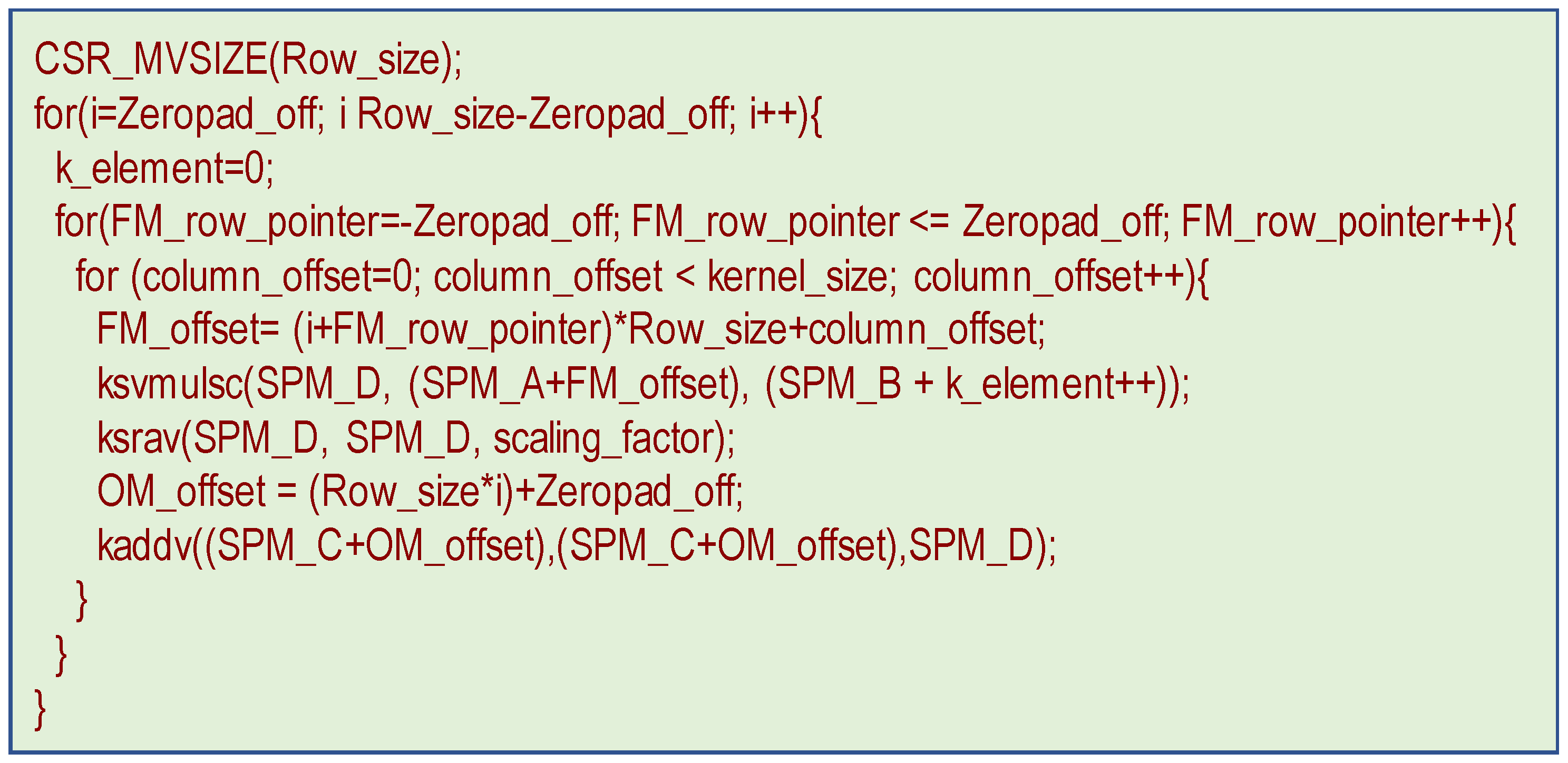
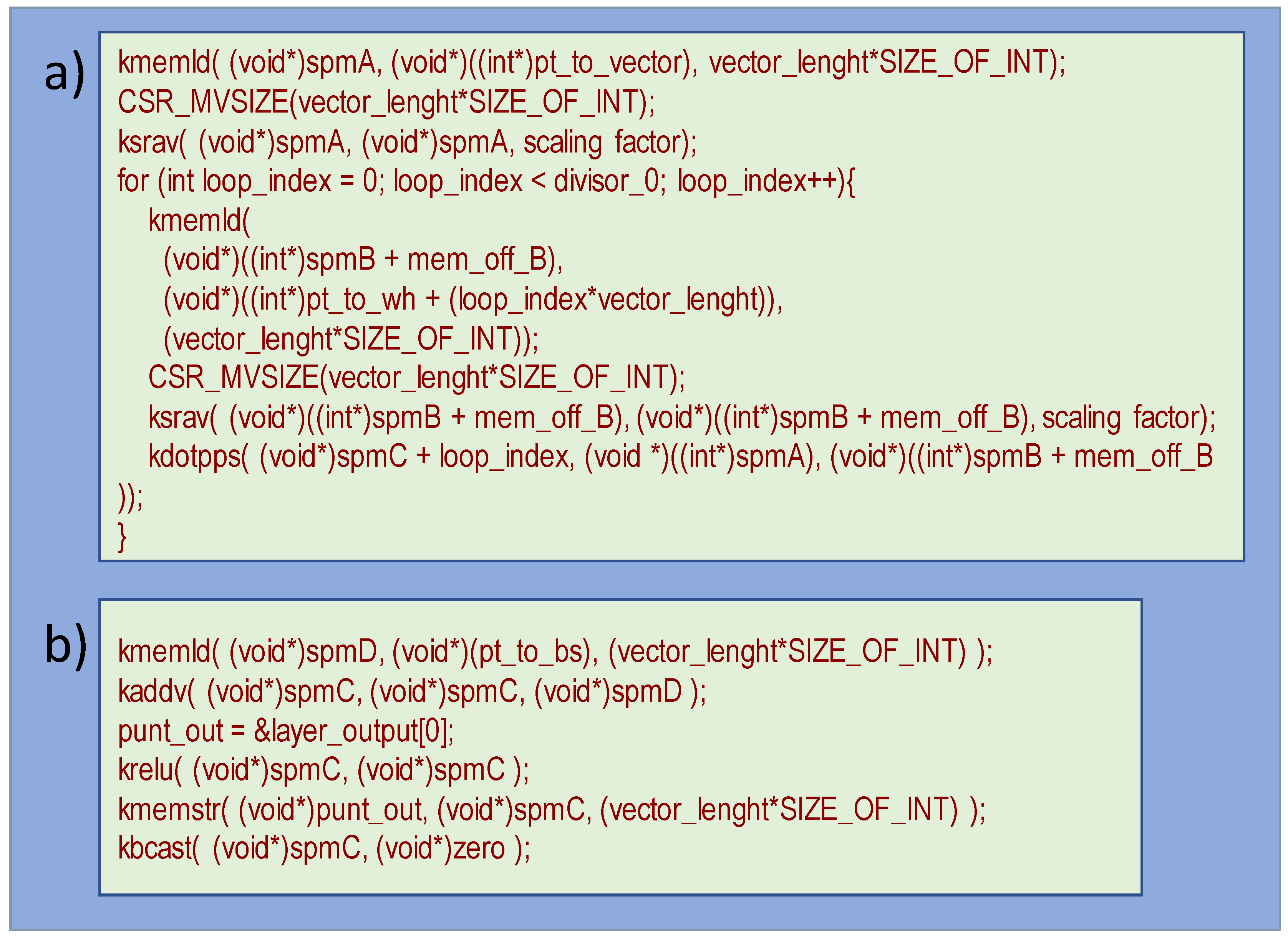
4.3. Vectorized C Code Implementation

Program code vectorization targeting the Klessydra intrinsic function library is based on two types of intervention: data movement to efficiently exploit the scratchpad memory sub-system, and vector arithmetic operation exploiting the accelerator functional unit.
A loop of kmemld() functions transfer the FM and KMs operands into two SPMs, that we refer to as spmA and spmB, from the main memory. To implement zero-padding, when loading the feature maps into spmA, we first reset the SPM content to zero and then proceed with loading bursts of data from the FM rows, with exact offsets that grant the correctness of zero-padding. Figure 10a displays the code executed to set up the FM in spmA. The offsets added to the pointers passed to the Kmemld() function allow for the implementation zero-padding. The ksrav() function implements fixed-point pre-scaling by performing an arithmetic right shift operation of a vector. It requires a pointer to the vector, a pointer to store the resulting vector and a shift amount Figure 10b similarly shows the loading and pre-scaling of the 9-element KM into spmB and also the calling sequence of the convolution2D() function.
The Convolution2D() function requires the addresses of the FM and KM first elements in spmA and spmB, an address pointing to a region in spmD for temporary value storage, and the address to store the output matrix in spmC. Figure 11 reports the internal operations, which are built upon knowing which vectors are to be multiplied as the kernel map slides across all the input map pixels. Taking into account which elements will be multiplied when the kernel completely slides across a row of the FM, and the fact that this process is replicated for every row, we can multiply the FM row values with the corresponding scalar from the KM, and update the output matrix (OM) row with a vector of partial results. This process is straightforward and allows to fully exploit the vector coprocessor capabilities by using matrix rows as vector operands.
Referring to Figure 11, after setting the vector length, the loop with index “i” scans the rows of the output matrix (OM); the FM_row_pointer loop and the column_offset loop iterates three times each to cover the necessary vector-scalar product required for the 3 × 3 kernel matrix. The FM_offset variable points to the proper FM row in spmA, from which the source vector is fetched. The ksvmulsc() function performs the scalar-vector multiplication between an FM row vector and a KM scalar, and the result is post-scaled by the ksrav() function for fixed-point alignment. The kaddv() function performs the vector addition, updating the OM row in spmC.
After the convolutions are done, the OM is updated with the addition of the bias value (Figure 12a). A kmemld() is required to have the single scalar value in the scratchpad memory, then the whole matrix is updated by ksvaddsc_v2(), which performs the vector plus scalar operation and includes a fourth parameter to adjust the vector length prior to doing the calculation.
As the last part of the convolutional layers, the ReLU non-linear function is applied to all the OM pixels, which is stored back in main memory. The SPM region is cleared for the next iteration of the loop by broadcasting a zero value into the target memory region with kbcast() (Figure 12b).
The maxpooling layer is executed on the OM in main memory, through conventional scalar instructions, following the same implementation of the generic C code.
The fully-connected layer is comprised of a computation kernel based on dot products (Figure 13a). The source vector is moved into spmA as a single burst of data using the kmemld() function, and pre-scaled by ksrav(). A loop handles the properly transposed loading of the neurons parameters into spmB. The two vectors in the SPMs are processed by the dot-product function kdotpps(), which includes a post-scaling of the product before accumulation for fixed point alignment.
After the end of the loop, the vector of bias values is moved into spmD then added to the output vector of the layer. The result vector is processed by the krelu() function, and then it is stored back to the main memory. The kbcast() function clears the spmC memory space (Figure 13b).
The softmax layer is executed in main memory through conventional scalar instructions, with the same implementation of the generic C code.
The exact execution of the vectorized VGG-16 inference program running on Klessydra T1 cores was verified by comparing the full output produced by RTL simulation against the general purpose VGG-16 fixed-point C code running on an X86 server.

5. Performance and Power Analysis
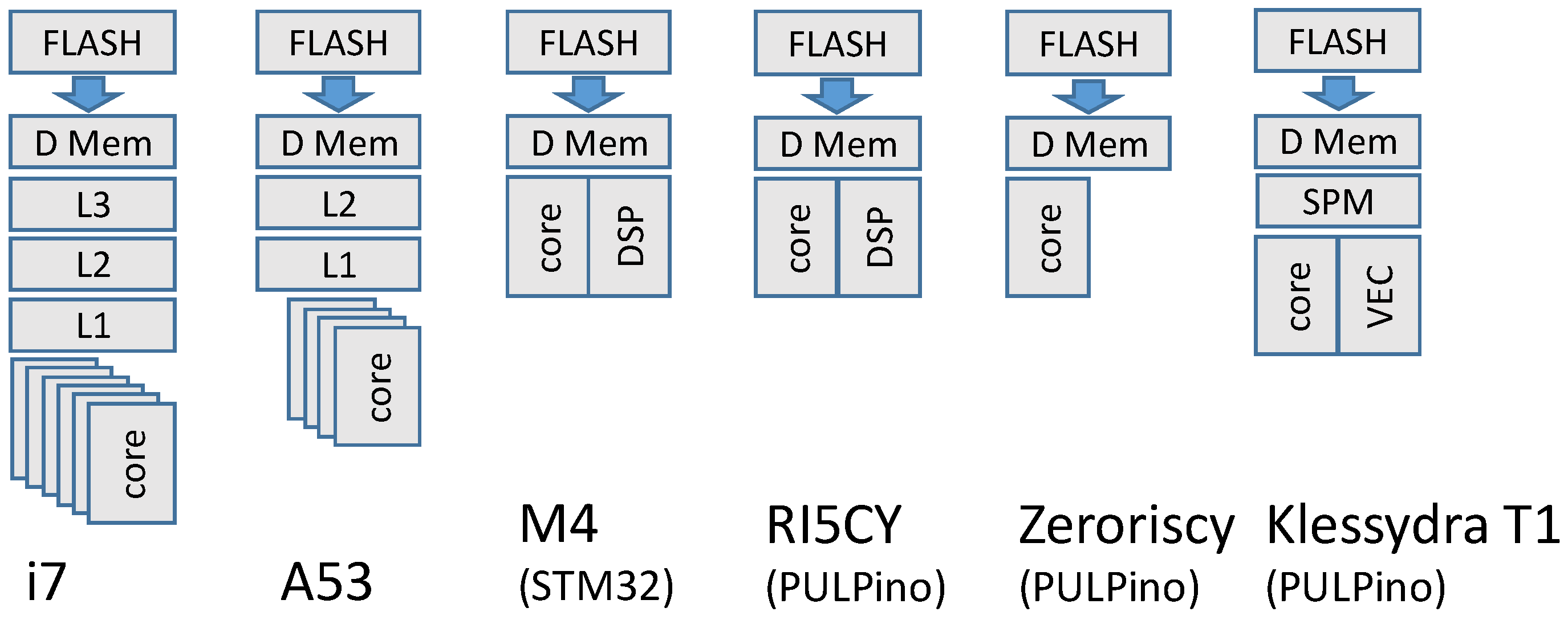
5.1. Setup

All Klessydra cores are compatible with the PULPino processor platform [25]. Yet, the original PULPino memory subsystem cannot support the execution of the full VGG-16 inference algorithm, which requires 255 MB storage for the constant data consisting of the neural network weights, and at least 1 MB memory space for global and local variables. Thus, we extended the PULPino memory sub-system to include 256 MB of addressable physical data memory, partitioned into a 1 cycle latency 1 MB RAM to be mapped on the FPGA BRAM, and a 6 cycle latency 255 MB space mapped on an external flash memory device, connected via SPI interface. The 1 MB RAM is the physical mapping of the portion of the data memory address space that is dedicated to dynamically allocated data.
The program memory is 32 KB mapped in the FPGA BRAM.
The modified PULPino platform featuring Klessydra T1 processor cores was synthesized on a Kintex7 FPGA from Xilinx integrated on the Genesys2 board from Digilent [28], using the Vivado tool flow. The design entry was the RTL VHDL/SystemVerilog description of the platforms under analysis. The C code of the VGG16 application was compiled by the RISC-V gcc tool chain to produce the binary code executable by the target processors. The execution of the application on the target processors was simulated both as RTL and post-synthesis gate level, to verify the correct functionality and to extract the signal activity for power estimation in Vivado. Table 4 reports the hardware resource utilization and the maximum clock frequency producing zero or positive slack, for all the processor configurations under analysis.
The VGG-16 inference fixed-point code was also implemented on the following alternative computing systems, to accomplish a comprehensive comparative analysis:
  • An FPGA board featuring a soft-processor comprised of the extended PULPino platform equipped with the DSP-accelerated RI5CY core, reaching 65 MHz clock frequency;
  • An FPGA board featuring a soft-processor comprised of the extended PULPino platform equipped with a Zeroriscy core [29], reaching 77 MHz clock frequency;
  • An STM32 single board computer featuring an 84 MHz ARM Cortex M4 core with DSP extension, 96 KB data memory;
  • A Raspberry-PI 3b+ single board computer featuring a 1.4 GHz ARM Cortex A53 quad-core CPU, 16 KB L1 cache and 512 KB L2 cache, 1 GB LPDDR2 main memory;
  • An x86 single board computer featuring a 3 GHz exa-core, 12-thread i7 CPU, 384 KB L1 cache, 1.5 MB L2 cache, 9 MB LLC, 8 GB DDR4 main memory.
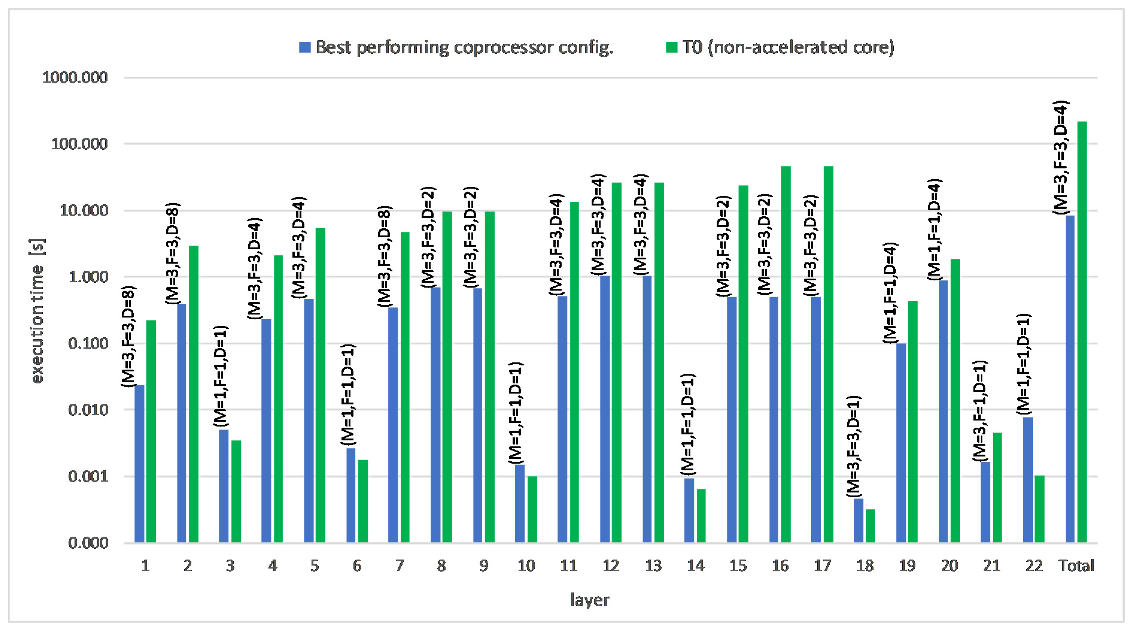
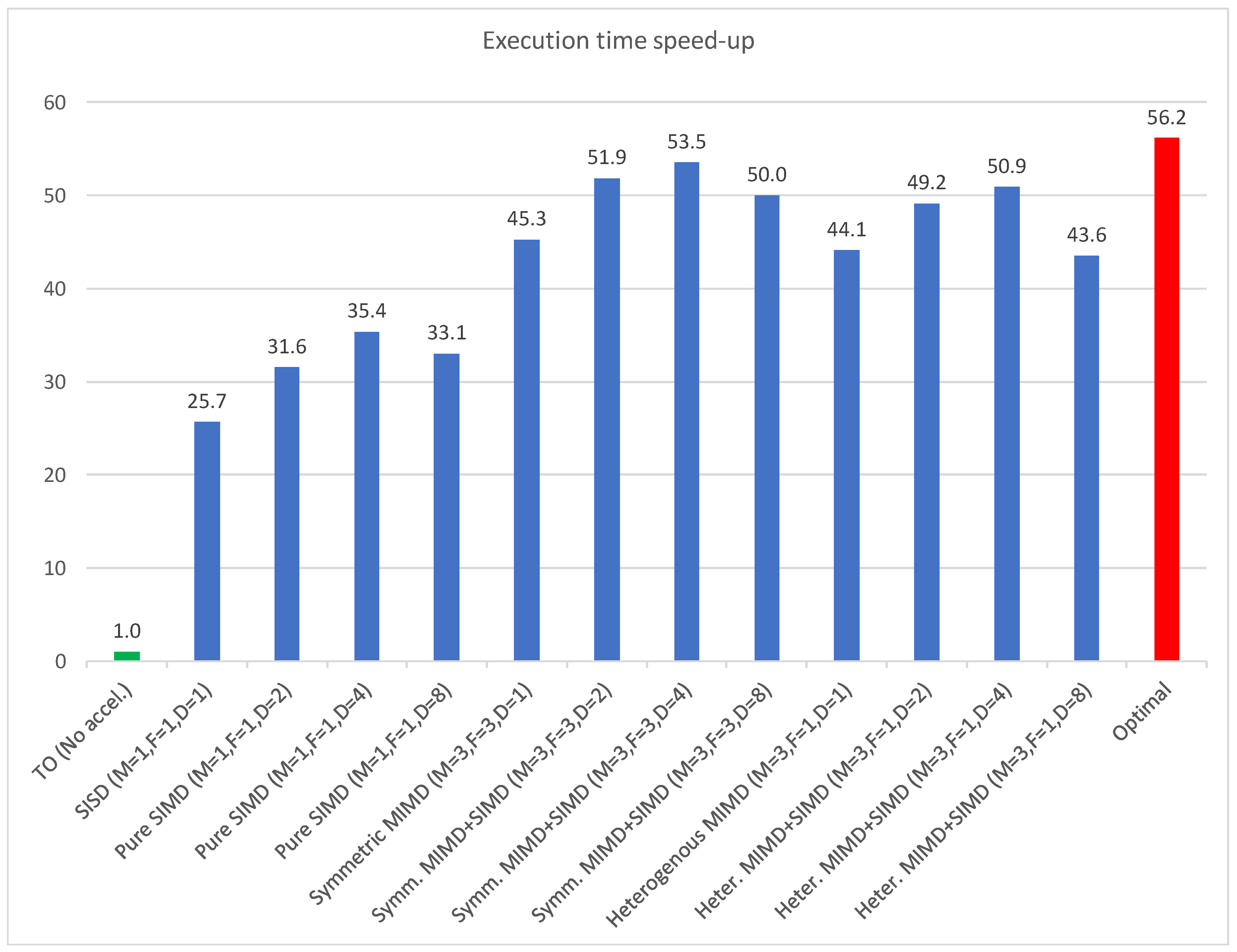
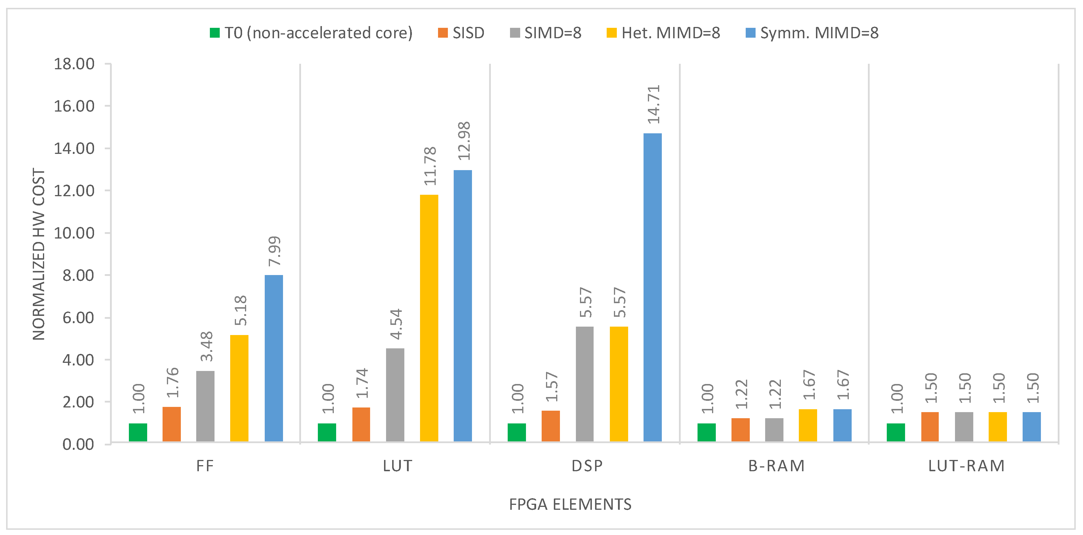
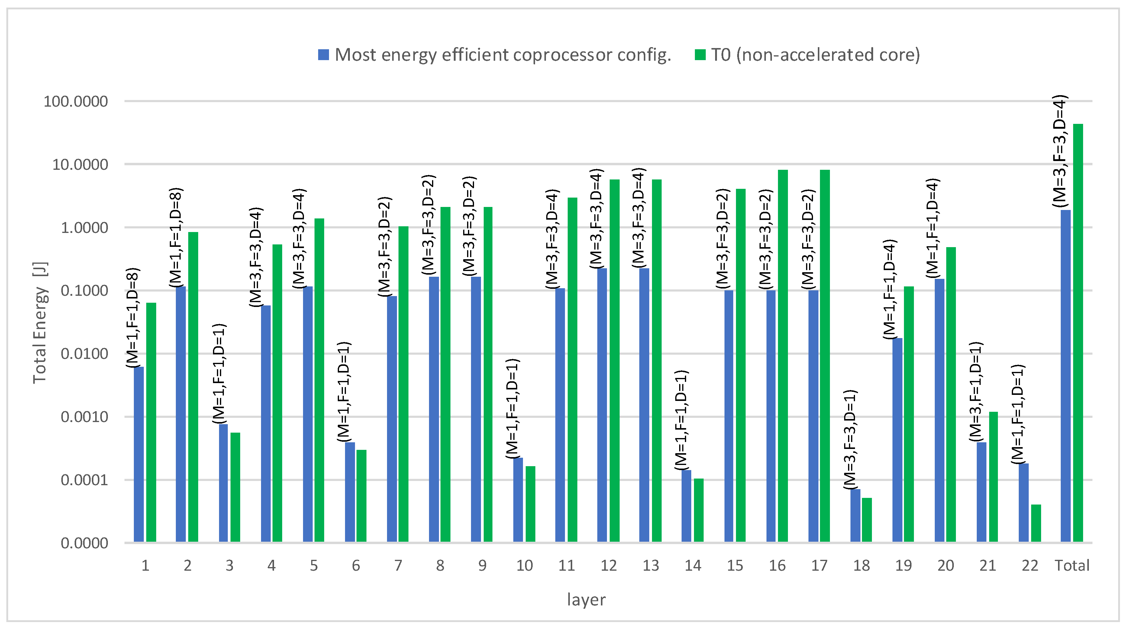
The system architecture organization corresponding to the devices under comparison are sketched in Figure 14. The read-only storage space dedicated to the VGG-16 weights is hosted by an SPI-connected Flash memory expansion board in all the considered architectures, and the weights are preemptively loaded into the main RAM space for the inference algorithm execution.

5.2. Results

The first phase of performance analysis targeted the detailed account of the performance of each coprocessor hardware microarchitecture.
Figure 15 shows the execution time obtained by the best performing of all the explored T1 coprocessor configurations and by the non-accelerated T0 core, for each VGG-16 layer. The results give evidence to the fact that the performance of the coprocessor hardware configurations varies with the algorithm layer it executes. The Symmetrical MIMD configurations with D ranging between 2 and 8 result to be the best performing for the convolutional layers, while the pure SIMD configurations with D = 4 results to be the optimal choice for the largest Fully Connected layers. Notably, the Maxpool and Softmax layers exhibit worse execution time in the accelerated cores than with in the non-accelerated T0 core, because in the present software implementation they are executed as scalar computation, and so the data transfer to/from the SPMs constitutes an overhead with no corresponding vector computation acceleration. Nonetheless, the relative impact of those layers on the overall execution time is negligible, as shown by the logarithmic scale.
Figure 16 presents the total VGG16 inference execution time speed-up obtained by each coprocessor configuration over the non-accelerated T0 core. The diagram also includes the ideal speed-up obtained assuming to use the optimal configuration for each layer. Figure 17 represents the hardware cost of the configurations that exhibit the highest speed-up, normalized to the non-accelerated T0 core hardware cost, for a direct comparison. The resulting hardware utilization efficiency is notable, as the maximum speed-up is over 50X, while the maximum hardware cost overhead is well below 15X.
Figure 18 shows the total energy consumed by the most efficient of all the explored T1 coprocessor configurations and by the non-accelerated T0 core, for each VGG-16 layer. Again, the optimal coprocessor configuration for energy efficiency depends on the layer being executed. Optimal energy efficiency, unlike absolute performance, swings between Pure SIMD and Symmetrical MIMD configurations. Similarly to the execution time analysis, for pure scalar computation layers the energy consumption worsens in the vector-accelerated microarchitecture, due to the SPM data transfer overhead. Yet, the overall impact of those layers on the total energy is negligible as shown by the logarithmic scale.
Figure 19 gives significance of the total energy saving obtained by each coprocessor configuration over the non-accelerated T0 core. The energy saving is expressed as the fraction of the energy consumed in the accelerated core over the energy consumed in the non-accelerated core, obtaining energy consumption between 6.4% and 4% of the non-accelerated core (energy saving between 93.6% and 96%). The diagram also includes the ideal energy reduction obtained assuming to use the optimal configuration for each layer.
Figure 16 and Figure 19 evidence the ideal performance limit achievable by dynamically changing the coprocessor microarchitecture at no overhead, via software controlled Dynamic Partial Reconfiguration (DPR) of the FPGA, so that the system always uses the optimal hardware scheme for speed or energy efficiency according to the computation kernel being executed. The storage, power and time overhead associated to DPR is not included in the analysis, and should be the subject of specific experiments.
The second phase of performance analysis aimed at comparing the efficiency of the proposed soft-processor architecture with the alternative hardware architecture solutions for the execution of the same application. In this analysis, the proposed solution consisted of the extended PULPino platform equipped with the Klessydra T1 core + optimal vector coprocessor for each layer being executed.
Table 5 summarizes the performance comparison results, expressed as total execution time, total energy consumption, and average energy consumed per algorithmic operation. Algorithmic operations are the data multiplications and additions that are inherent to the algorithm being computed, and do not depend on the actual software implementation. The absolute execution time obviously favors high-end computing devices, yet the results give evidence of the effectiveness of the Klessydra T1 customizable vector coprocessor sub-system with respect to other single-core PULPino soft-processor FPGA implementations. Additionally, the energy efficiency results show the potential advantage of a Klessydra T1 vector-accelerated soft-processor FPGA implementation, with respect to general purpose single-board computers.

6. Conclusions

The validation of the VGG-16 inference output data produced by Klessydra processors against conventional processors demonstrated how the Klessydra open-source infrastructure can be used for implementing configurable RISC-V soft-cores equipped with hardware acceleration for vector computing on FPGA. The detailed porting of the target application routines has been documented in this work. Performance results show the effectiveness of the Klessydra microarchitecture scheme, built upon interleaved multi-threading and vector coprocessor hardware acceleration, with respect to other FPGA-based single-core solutions. Looking at energy efficiency, the Klessydra FPGA soft-core solution shows superior performance with respect to commercial single-board computers that may be used as IoT extreme-edge devices.
The results of the performance analysis conducted on the Klessydra T1 vector coprocessor schemes demonstrate the dependency of the optimal hardware configuration on the algorithm’s layer being executed. This evidence opens the way to the development of software configurable accelerators and further to the implementation of self-adapting coprocessor microarchitectures in IoT extreme-edge nodes.

Supplementary Materials

The Klessydra processor core family and accelerators are openly available online at https://www.github.com/klessydra.

Author Contributions

Conceptualization, M.O.; methodology, M.O. and A.C.; hardware design and Synthesis, A.C.; software, S.S.; validation, A.C. and S.S.; formal analysis, S.S.; investigation, A.C.; data curation, A.C. and S.S.; tool maintenance, A.M.; writing—original draft preparation, M.O.; writing—review and editing, A.C., A.M., and F.M.; visualization, A.C.; supervision, M.O.; project administration, M.O.; funding acquisition, M.O. All authors have read and agreed to the published version of the manuscript.

Funding

This research was supported by a Sapienza University internal research grant.

Data Availability Statement

Data is contained within the article.

Conflicts of Interest

The authors declare no conflict of interest.

References

  1. Samie, F.; Bauer, L.; Henkel, J. From Cloud Down to Things: An Overview of Machine Learning in Internet of Things. IEEE Internet Things J. 2019, 4662, 1. [Google Scholar] [CrossRef]
  2. European Processor Intiative (EPI). EU H2020 Research and Innovation Programme GA No 826647. Available online: https://www.european-processor-initiative.eu/project/epi/ (accessed on 26 January 2021).
  3. RISC-V. Instruction Set Specifications. Available online: https://riscv.org/specifications/ (accessed on 26 January 2021).
  4. Cheikh, A.; Sordillo, S.; Mastrandrea, A.; Menichelli, F.; Scotti, G.; Olivieri, M. Klessydra-T: Designing Vector Coprocessors for Multi-Threaded Edge-Computing Cores. IEEE Micro 2021, 1. [Google Scholar] [CrossRef]
  5. Gautschi, M.; Schiavone, P.; Traber, A.; Loi, I.; Pullini, A.; Rossi, D.; Flamand, E.; Gürkaynak, F.; Benini, L. Near-threshold RISC-V core with DSP extensions for scalable IoT endpoint devices. IEEE Trans. Very Large Scale Integr. (VLSI) Syst. 2017, 25, 2700–2713. [Google Scholar] [CrossRef] [Green Version]
  6. Seo, S.; Dreslinski, R.G.; Woh, M.; Chakrabarti, C.; Mahlke, S.; Mudge, T. Diet SODA: A power-efficient processor for digital cameras. In Proceedings of the 16th ACM/IEEE International Symposium on Low Power Electronics and Design, Austin, TX, USA, 18–20 August 2010; pp. 79–84. [Google Scholar]
  7. Chen, Y.H.; Krishna, T.; Emer, J.S.; Sze, V. Eyeriss: An energy-efficient reconfigurable accelerator for deep convolutional neural networks. IEEE J. Solid-State Circuits 2016, 52, 127–138. [Google Scholar] [CrossRef] [Green Version]
  8. Moini, S.; Alizadeh, B.; Emad, M.; Ebrahimpour, R. A resource-limited hardware accelerator for convolutional neural networks in embedded vision applications. IEEE Trans. Circuits Syst. II Express Briefs 2017, 64, 1217–1221. [Google Scholar] [CrossRef]
  9. Conti, F.; Benini, L. A ultra-low-energy convolution engine for fast brain-inspired vision in multicore clusters. In Proceedings of the IEEE Design, Automation and Test in Europe Conference and Exhibition (DATE), Grenoble, France, 9–13 March 2015; pp. 683–688. [Google Scholar]
  10. Meloni, P.; Deriu, G.; Conti, F.; Loi, I.; Raffo, L.; Benini, L. Curbing the roofline: A scalable and flexible architecture for CNNs on FPGA. In Proceedings of the ACM International Conference on Computing Frontiers, Como, Italy, 16–18 May 2016; pp. 376–383. [Google Scholar]
  11. Wu, N.; Jiang, T.; Zhang, L.; Zhou, F.; Ge, F. A Reconfigurable Convolutional Neural Network-Accelerated Coprocessor Based on RISC-V Instruction Set. Electronics 2020, 9, 1005. [Google Scholar] [CrossRef]
  12. Watanabe, D.; Yano, Y.; Izumi, S.; Kawaguchi, H.; Takeuchi, K.; Hiramoto, T.; Iwai, S.; Murakata, M.; Yoshimoto, M. An Architectural Study for Inference Coprocessor Core at the Edge in IoT Sensing. In Proceedings of the 2nd IEEE International Conference on Artificial Intelligence Circuits and Systems (AICAS), Genoa, Italy, 23–25 March 2020; pp. 305–309. [Google Scholar]
  13. Wu, Y.; Wang, J.J.; Qian, K.; Liu, Y.; Guo, R.; Hu, S.G.; Yu, Q.; Chen, T.P.; Liu, Y.; Rong, L. An energy-efficient deep convolutional neural networks coprocessor for multi-object detection. Microelectron. J. 2020, 98, 104737. [Google Scholar] [CrossRef]
  14. Chang, M.C.; Pan, Z.G.; Chen, J.L. Hardware accelerator for boosting convolution computation in image classification applications. In Proceedings of the 2017 IEEE 6th Global Conference on Consumer Electronics (GCCE), Nagoya, Japan, 24–27 October 2017; pp. 1–2. [Google Scholar]
  15. Lima, P.; Vieira, C.; Reis, J.; Almeida, A.; Silveira, J.; Goerl, R.; Marcon, C. Optimizing RISC-V ISA Usage by Sharing Coprocessors on MPSoC. In Proceedings of the 2020 IEEE Latin-American Test Symposium (LATS), Maceio, Brazil, 30 March–2 April 2020; pp. 1–5. [Google Scholar]
  16. Du, L.; Du, Y.; Li, Y.; Su, J.; Kuan, Y.C.; Liu, C.C.; Chang, M.C.F. A reconfigurable streaming deep convolutional neural network accelerator for Internet of Things. IEEE Trans. Circuits Syst. I Regul. Pap. 2018, 65, 198–208. [Google Scholar] [CrossRef] [Green Version]
  17. Olivieri, M.; Cheikh, A.; Cerutti, G.; Mastrandrea, A.; Menichelli, F. Investigation on the optimal pipeline organization in RISC-V multi-threaded soft processor cores. In 2017 New Generation of CAS (NGCAS); IEEE: New York, NY, USA, 2017; pp. 45–48. [Google Scholar]
  18. Cheikh, A.; Sordillo, S.; Mastrandrea, A.; Menichelli, F.; Olivieri, M. Efficient Mathematical Accelerator Design Coupled with an Interleaved Multi-threading RISC-V Microprocessor. In Proceedings of the International Conference on Applications in Electronics Pervading Industry, Environment and Society, Pisa, Italy, 11–13 September 2019; Springer: Cham, Switzerland, 2019; pp. 529–539. [Google Scholar]
  19. Lattner, C. RISC-V Vector Extension Intrinsic Support. Available online: https://www.sifive.com/blog/risc-v-vector-extension-intrinsic-support (accessed on 26 January 2021).
  20. Cavalcante, M.; Schuiki, F.; Zaruba, F.; Schaffner, M.; Benini, L. Ara: A 1-GHz+ Scalable and Energy-Efficient RISC-V Vector Processor with Multiprecision Floating-Point Support in 22-nm FD-SOI. IEEE Trans. Very Large Scale Integr. (VLSI) Syst. 2020, 28, 530–543. [Google Scholar] [CrossRef] [Green Version]
  21. Chen, C.; Xiang, X.; Liu, C.; Shang, Y.; Guo, R.; Liu, D.; Lu, Y.; Hao, Z.; Luo, J.; Chen, Z.; et al. Xuantie-910: A Commercial Multi-Core 12-Stage Pipeline Out-of-Order 64-bit High Performance RISC-V Processor with Vector Extension: Industrial Product. In Proceedings of the 2020 ACM/IEEE 47th Annual International Symposium on Computer Architecture (ISCA), Valencia, Spain, 30 May–3 June 2020; pp. 52–64. [Google Scholar]
  22. Wright, J.C.; Schmidt, C.; Keller, B.; Dabbelt, D.P.; Kwak, J.; Iyer, V.; Mehta, N.; Chiu, P.-F.; Bailey, S.; Asanovic, K.; et al. A Dual-Core RISC-V Vector Processor with On-Chip Fine-Grain Power Management in 28-nm FD-SOI. IEEE Trans. Very Large Scale Integr. (VLSI) Syst. 2020, 28, 2721–2725. [Google Scholar] [CrossRef]
  23. Kimura, Y.; Kikuchi, T.; Ootsu, K.; Yokota, T. Proposal of Scalable Vector Extension for Embedded RISC-V Soft-Core Processor. In Proceedings of the 7th International Symposium on Computing and Networking Workshops (CANDARW), Nagasaki, Japan, 26–29 November 2019; pp. 435–439. [Google Scholar]
  24. Johns, M.; Kazmierski, T.J. A Minimal RISC-V Vector Processor for Embedded Systems. In Proceedings of the 2020 Forum for Specification and Design Languages (FDL), Kiel, Germany, 15–17 September 2020. [Google Scholar]
  25. Traber, A.; Gautschi, M. PULPino: Datasheet; ETH: Zurich, Switzerland; University of Bologna: Bologna, Italy, 2017; Available online: https://pulp-platform.org/docs/pulpino_datasheet.pdf (accessed on 26 January 2021).
  26. Blasi, L.; Vigli, F.; Cheikh, A.; Mastrandrea, A.; Menichelli, F.; Olivieri, M. A RISC-V Fault-Tolerant Microcontroller Core Architecture Based on a Hardware Thread Full/Partial Protection and a Thread-Controlled Watch-Dog Timer. In Proceedings of the International Conference on Applications in Electronics Pervading Industry, Environment and Society, Pisa, Italy, 11–13 September 2019; Springer: Cham, Switzerland, 2019; pp. 505–511. [Google Scholar]
  27. Cheikh, A.; Cerutti, G.; Mastrandrea, A.; Menichelli, F.; Olivieri, M. The microarchitecture of a multi-threaded RISC-V compliant processing core family for IoT end-nodes. In Proceedings of the International Conference on Applications in Electronics Pervading Industry, Environment and Society, Rome, Italy, 21–22 September 2017; Springer: Cham, Switzerland, 2017; pp. 89–97. [Google Scholar]
  28. Genesys 2 Kintex-7 FPGA Development Board. Available online: https://reference.digilentinc.com/reference/programmable-logic/genesys-2/start?redirect=1 (accessed on 26 January 2021).
  29. Schiavone, P.D.; Conti, F.; Rossi, D.; Gautschi, M.; Pullini, A.; Flamand, E.; Benini, L. Slow and steady wins the race? A comparison of ultra-low-power risc-v cores for internet-of-things applications. In Proceedings of the 27th International Symposium on Power and Timing Modeling, Optimization and Simulation (PATMOS), Thessaloniki, Greece, 25–27 September 2017; pp. 1–8. [Google Scholar]
Figure 1. Klessydra T0 core microarchitecture.
Electronics 10 00518 g001
Figure 2. Klessydra T1 core microarchitecture.
Electronics 10 00518 g002
Figure 3. Hart interleaving and hart stall timing diagram.
Electronics 10 00518 g003
Figure 4. Code for multi-threaded execution on Klessydra-T1.
Electronics 10 00518 g004
Figure 5. Klessydra T1 memory map.
Electronics 10 00518 g005
Figure 6. Workflow for the VGG-16 implementation.
Electronics 10 00518 g006
Figure 7. (a) Convolutional layer in generic C code; (b) Convolution2D function inner operations; (c) Bias addition and ReLU function inner operations (Layers: 1, 2, 4, 5, 7, 8, 9, 11, 12, 13, 15, 16, 17).
Electronics 10 00518 g007
Figure 8. (a) Maxpool layer in generic C code; (b) Maxpool function inner operations (Layers: 3, 6, 10, 14, 18).
Electronics 10 00518 g008
Figure 9. (a) Fully-connected layer in generic C code; (b) Fully-connect inner operations; (c) Softmax layer inner operations (Fully-connected Layer: 19, 20, 21; Softmax Layer: 22).
Electronics 10 00518 g009
Figure 10. (a) Zero-padded, pre-scaled FM setup in SPM; (b) Pre-scaled KM collection in SPM and calling sequence of convolution2D() (Layers: 1, 2, 4, 5, 7, 8, 9, 11, 12, 13, 15, 16, 17).
Electronics 10 00518 g010
Figure 11. Convolution2D inner loops operations (Layers: 1, 2, 4, 5, 7, 8, 9, 11, 12, 13, 15, 16, 17).
Electronics 10 00518 g011
Figure 12. (a) Adding the bias to the Output Matrix; (b) Applying the ReLu function to the Output Matrix (Layers: 1, 2, 4, 5, 7, 8, 9, 11, 12, 13, 15, 16, 17).
Electronics 10 00518 g012
Figure 13. Fully-connected layer operations. (a) Dot-product kernel; (b) Bias addition and ReLu (Fully-connected Layer: 19, 20, 21).
Electronics 10 00518 g013
Figure 14. System architecture organization of the compared boards.
Electronics 10 00518 g014
Figure 15. Absolute execution time [s] of the best performing accelerated configuration and of the non-accelerated T0 core, per layer.
Electronics 10 00518 g015
Figure 16. Total execution time speed-up over non-accelerated core obtained by each coprocessor configuration, along with the speed-up obtained by using the optimal configuration for each layer.
Electronics 10 00518 g016
Figure 17. Hardware overhead normalized to the non-accelerated T0 core.
Electronics 10 00518 g017
Figure 18. Total energy consumption [J] of the most energy efficient coprocessor configuration and of the non-accelerated T0 core, per layer.
Electronics 10 00518 g018
Figure 19. Energy reduction factor with respect to non-accelerated core (lower is better) obtained by each coprocessor configuration, along with the energy obtained by using the optimal configuration for each layer.
Electronics 10 00518 g019
Table 1. Summary of explored hardware configurations.
M (Number of SPMI Units)F (Number of FUs)D (Number of Lanes in Each FU)Execution Paradigm
111SISD
112, 4, 8Pure SIMD
331Symmetric MIMD
332, 4, 8Symmetric MIMD + SIMD
311Heterogenous MIMD
312, 4, 8Heterogenous MIMD + SIMD
Table 2. RISC-V instruction set custom extension for Klessydra-T processors.
Assembly Syntax—(r) Denotes Memory Addressing via Register rFunction DeclarationShort Description
kmemld (rd), (rs1), (rs2)kmemld((void*) rd, (void*) rs1, (int) rs2)load vector into scratchpad region
kmemstr (rd), (rs1), (rs2)kmemstr((void*) rd, (void*) rs1, (int) rs2)store vector into main memory
kaddv (rd), (rs1), (rs2)kaddv((void*) rd, (void*) rs1, (void*) rs2)adds vectors in scratchpad region
ksubv (rd), (rs1), (rs2)ksubv((void*) rd, (void*) rs1, (void*) rs2)subtract vectors in scratchpad region
kvmul (rd), (rs1), (rs2)kvmul((void*) rd, (void*) rs1, (void*) rs2)multiply vectors in scratchpad region
kvred (rd), (rs1)kvred((void*) rd, (void*) rs1)reduce vector by addition
kdotp (rd), (rs1), (rs2)kdotp((void*) rd, (void*) rs1, (void*) rs2)vector dot product into register
ksvaddsc (rd), (rs1), (rs2)ksvaddsc((void*) rd, (void*) rs1, (void*) rs2)add vector + scalar into scratchpad
ksvaddrf (rd), (rs1), rs2ksvaddrf((void*) rd, (void*) rs1, (int) rs2)add vector + scalar into register
ksvmulsc (rd), (rs1), (rs2)ksvmulsc((void*) rd, (void*) rs1, (void*) rs2)multiply vector + scalar into scratchpad
ksvmulrf (rd), (rs1), rs2ksvmulrf((void*) rd, (void*) rs1, (int) rs2)multiply vector + scalar into register
kdotpps (rd), (rs1), (rs2)kdotpps((void*) rd, (void*) rs1, (void*) rs2)vector dot product and post scaling
ksrlv (rd), (rs1), rs2ksrlv((void*) rd, (void*) rs1, (int) rs2)vector logic shift within scratchpad
ksrav (rd), (rs1), rs2ksrav((void*) rd, (void*) rs1, (int) rs2)vector arithmetic shift within scratchpad
krelu (rd), (rs1)krelu((void*) rd, (void*) rs1)vector ReLu within scratchpad
kvslt (rd), (rs1), (rs2)kvslt((void*) rd, (void*) rs1, (void*) rs2)compare vectors and create mask vector
ksvslt (rd), (rs1), rs2ksvslt((void*) rd, (void*) rs1, (int) rs2)compare vector-scalar and create mask
kvcp (rd), (rs1)ksrlv((void*) rd, (void*) rs1)copy vector within scratchpad region
csr MVSIZE, rs1mvsize((int) rs1)vector length setting
csr MVTYPE, rs1mvtype((int) rs1)element width setting (8, 16, 32 bits)
csr MPSCLFAC, rs1mpsclfac((int) rs1)post scaling factor (kdotpps instruction)
Table 3. Cifar-10 VGG-16 inference layers.
Layer NumberComputation TypeMatrix Size
1Convolution32 × 32
2Convolution32 × 32
3Max Pool16 × 16
4Convolution16 × 16
5Convolution16 × 16
6Max Pool8 × 8
7Convolution8 × 8
8Convolution8 × 8
9Convolution8 × 8
10Max Pool4 × 4
11Convolution4 × 4
12Convolution4 × 4
13Convolution4 × 4
14Max Pool2 × 2
15Convolution2 × 2
16Convolution2 × 2
17Convolution2 × 2
18Max Pool1 × 1
19Fully connected512 × 512
20Fully connected4096 × 4096
21Fully connected4096 × 4096
22Softmax10
Table 4. Area and frequency summary of the Klessydra-T cores equipped with to 1 MB Data Mem.
ConfigurationHardware UtilizationTop Freq. [MHz]
FFLUTDSPB-RAMLUT-RAM
SISD (M = 1, F = 1, D = 1)248270831188264132.1
Pure SIMD (M = 1, F = 1, D = 2)266490101588264127.0
Pure SIMD (M = 1, F = 1, D = 4)351011,6782388264125.5
Pure SIMD (M = 1, F = 1, D = 8)490418,5313988264112.6
Symmetric MIMD (M = 3, F = 3, D = 1)350910,70119120264114.2
Symmetric MIMD+SIMD (M = 3, F = 3, D = 2)465916,55631120264113.9
Symmetric MIMD+SIMD (M = 3, F = 3, D = 4)674627,48555120264108.9
Symmetric MIMD+SIMD (M = 3, F = 3, D = 8)11,25352,93010312026496.3
Heterogenous MIMD (M = 3, F = 1, D = 1)302510,65511120264119.9
Heterogenous MIMD+SIMD (M = 3, F = 1, D = 2)374117,16115120264115.7
Heterogenous MIMD+SIMD (M = 3, F = 1, D = 4)476725,53523120264110.4
Heterogenous MIMD+SIMD (M = 3, F = 1, D = 8)730348,0663912026491.5
T0 (No accl)14094079772176194.6
RI5CY13076351672065.1
Zeroriscy16052834172077.2
Table 5. Performance comparison with alternative solutions.
ProcessorTime [s]Energy [J]Energy per op [pJ/op]
Core i7 PC board0.082.9021
Cortex A53 Raspberry Pi 30.892.3217
Cortex M4 STM32117.787.7755
RI5CY PULPino on FPGA444.3040.06285
Zeroriscy PULPino on FPGA548.0438.90277
Klessydra-T1 PULPino on FPGA7.911.7412
Publisher’s Note: MDPI stays neutral with regard to jurisdictional claims in published maps and institutional affiliations.

