Abstract
The high frequency transformer in single-phase full-bridge DC-DC converter is prone to saturation because of the asymmetry of circuit parameters. Transformer saturation will increase power consumption, accelerate the aging of winding insulation, and even damage power switches. In order to prevent this risk, a DC bias suppression strategy is presented in this article, and the main advantage of this strategy is that the problem of transformer saturation can be completely eliminated. In this article, firstly, the DC bias and saturation mechanism of single-phase full-bridge DC-DC converter are analyzed in detail, and the Maximum Integral Value of Volt-Second Product error (MIVVSPE) is derived. Secondly, aiming at the saturation problem of single-phase full bridge DC-DC converter, a new digital integral circuit is designed to evaluate the DC bias state of transformer, and a DC bias suppression strategy is constructed to suppress the saturation of transformer. Furthermore, different from the traditional current feedback control strategy, the DC bias suppression strategy based on volt-second product error integral can be triggered before the transformer enters the saturation state, and the transformer saturation can be completely suppressed. Finally, a 30 kW single-phase full-bridge DC-DC converter for arc welding is established in lab. The experimental results show that the new DC bias suppression strategy can effectively prevent the transformer from entering the saturation state and improve the operation stability of single-phase full-bridge DC-DC arc welding inverter.
1. Introduction
With the rapid development of power electronic technology, high efficiency low voltage and high current arc welding inverter have been widely used in industrial production [1,2]. The single-phase full-bridge DC-DC converter topology has higher power processing capacity and makes better use of transformer core and power switch, which fully meets the requirements of modern arc welding machine, and it has become a research hotspot in the field of welding power supply [3,4,5].
The asymmetry of circuit parameters is one of the main reasons for DC bias of single-phase full-bridge DC-DC converter. For example, the non-synchronization of the driving signals and the difference of the turn on/off delay of IGBT will lead to unequal pulse width in the transformer input voltage. Moreover, the difference in the on-state resistance of IGBT will cause the asymmetry of the input voltage amplitude of the transformer. When the input voltage of the transformer is asymmetrical in amplitude and pulse width, the volt-second product on the primary side will enter an unbalanced state, and then the transformer will operate in the DC bias state [6,7,8]. In most arc welding applications, the frequent short circuit and no-load makes the DC bias more serious, which increases the risk of transformer saturation and reduces the reliability of arc welding inverter [9].
In order to solve this problem, various methods have been proposed, which can be divided into hardware topology optimization method [10,11,12,13,14] and software optimization method [15,16,17,18,19,20,21,22,23,24]. The hardware topology optimization method is to improve the anti-DC bias ability by adjusting the structure and parameters of the hardware topology, which belongs to the active suppression method. The “DC blocking capacitor” is usually connected in series with the primary winding of the transformer to prevent DC bias. However, the DC bias suppression ability of the DC-blocking capacitor is proportional to the capacity of the selected capacitor. When the capacity is small, the DC bias suppression ability is stronger, but the partial voltage on the capacitor is also larger, which will reduce the energy conversion efficiency of the inverter. When the capacity is large, it can only restrain the DC bias caused by the slowly changing volt-second product imbalance, but has little inhibitory effect on the DC bias caused by the fast-changing volt-second product imbalance. In addition, It is also feasible to introduce an air-gap into the circuit. Because the permeability of the non-magnetic material is lower, it needs a higher H to obtain the same B compared with the soft magnetic material. Therefore, the air-gap increases the value of magnetization current and lowers the achievable flux density. However, due to increased reluctance of an air gap the flux spreads into the surrounding medium causing the flux fringing effect. It is generally an unwanted phenomenon which usually increases proximity and eddy current loss in conductors located in the vicinity of the air gap. The essence of the software optimization method is a closed-loop optimization control strategy, where the control variable is the duty cycle of the full-bridge drive pulse, and the feedback variable is the primary current of the transformer. When the transformer enters the saturation state, a large current pulse will be generated in the primary current, and, if the current pulse exceeds the reference current, the DC bias suppression strategy will be triggered. Therefore, this method belongs to passive suppression method. In addition, in the suppression strategy, the adjustment mode and depth of duty cycle do not depend on the degree of saturation, and the feedback current is only used to trigger the adjustment strategy; therefore, the software optimization method is blind and has poor reliability in the treatment of transformer saturation.
The main contribution of this article is to analyze the saturation mechanism of transformer in detail, and the mathematical expression of the Maximum Integral Value of Volt-Second Product Error (MIVVSPE) is derived. Then, on the basis of theoretical analysis and mathematical derivation, a DC bias suppression method to prevent transformer saturation is proposed. In the rest of the paper, the mechanism of transformer saturation is analyzed, and the MIVVSPE expression is derived in Section 2. The proposed DC bias suppression strategy, including the circuit design method, is presented in Section 3. Then, in Section 4, a 30 kW single-phase full-bridge DC-DC converter for arc welding is established to verify the effectiveness of the suppression strategy. Finally, the conclusion of the paper is drawn in Section 5.
2. Generation Mechanism of MIVVSPE
A circuit of the single-phase full-bridge DC-DC converter is depicted in Figure 1 [25]. It is composed of an inverter and a rectifier. The inverter consists of a high frequency transformer and four IGBTs used as controllable switches , , , and , where, in order to simplify the analysis process, the transformer is modeled by an ideal transformer, and its magnetizing inductance , the leakage inductances, and stray capacitances are neglected. The transistors in each switching leg are driven by nonoverlapping voltages that are out of phase by . The maximum duty cycle of the gate-to-source voltages is slightly less than . The waveforms of the gate-to-source voltages should not overlap each other to avoid cross conduction [26]. When and are on, and are turned off, and the current path is A (+) → Q1 → the primary side of transformer → Q4 → B (−), and the voltage at the primary side is , and turn off, and bears forward voltage. When and are turned off, the voltage polarity at the primary side is reversed, and the stored energy of the transformer is released through the freewheeling diode , capacitor and diode . At this moment, there is no voltage drop in and , and and bear forward voltage. In this process, the energy release is faster, and the voltage amplitude of and will decay quickly. When the current on the primary side is zero, and are turned on, and the current is reversed. When and are turned off again, the above process will be repeated.
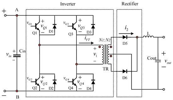
Figure 1.
The single-phase full-bridge DC-DC converter with a transformer center-tapped rectifier.
2.1. Saturation Mechanism Analysis
Figure 2 shows the key waveforms in the single-phase full-bridge DC-DC converter with a transformer center-tapped rectifier for continuous conduction mode.
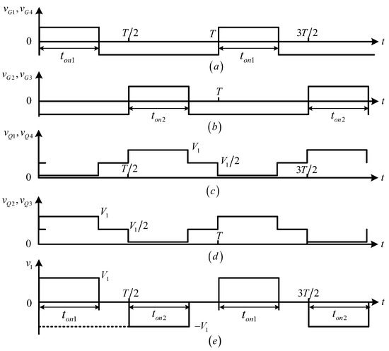
Figure 2.
The key waveforms in the single-phase full-bridge DC-DC converter: (a,b) represent the gating signals for and , , and , respectively. (c,d) represent the across voltages of and , , and , respectively. (e) The voltage across the primary winding .
During the time interval , the switches and , as well as the diode , are on, whereas the switches and , as well as the diode , are off, and the voltage across the primary winding is:
Similarly, within time interval , the voltage across the primary winding can be expressed as:
where , , , and represents the voltages across , , , and , respectively.
Assume that the IGBTs are ideal switches. Then, the on-resistance of IGBTs are equal, such that ; therefore, the amplitudes of are equal during the positive half-wave (Equation (1)) and the negative half-wave (Equation (2)). At the same time, the turn on/off delay are the same, and there is no difference between gate drive signals, so that the pulse width is also equal , where represents the duty cycle of . Therefore, the volt-second product can be expressed as:
According to Equation (3), the magnetic induction can be expressed as:
where represents the cross-sectional area of the transformer core, and represents the number of turns of the primary side of the transformer.
However, in most applications, the circuit parameters of single-phase full-bridge DC-DC converter are often asymmetric, such as the slight difference in gate drive signals, turn-on/turn-off delay, and on-resistance of IGBTs. The asymmetry of the gate drive signals or the difference in turn on/off delay of IGBTs will result in pulse width imbalance. As shown in Figure 3a, the turn-off delay of and is greater than that of and , so that the positive pulse width is increased to . And the non-uniformity in on-resistance of IGBTs will lead to the across voltages ∼ to be unequal, according to Equations (1) and (2), and it will result in amplitude unbalance. As shown in Figure 3b, the on-resistance of and is less than that of and , so that the positive amplitude of is increased to . If the above two unbalance conditions exist at the same time, the voltage across the primary winding is shown in Figure 3c. Furthermore, when the negative imbalance occurs, the change of the amplitude and pulse width of in the negative half wave is the same as that in the positive half wave of in Figure 3.
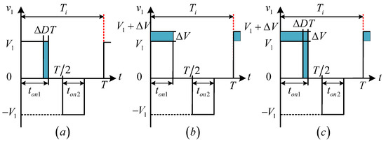
Figure 3.
The voltage across the primary winding under positive unbalanced conditions: (a) The pulse width imbalance. (b) The amplitude unbalance. (c) Both pulse width and amplitude are unbalanced.
If the inverter meets the unbalance condition shown in Figure 3, the volt-second product will produce an error in the switching period :
Therefore, the magnetic induction error in the switching period can be expressed as:
When , the curve is no longer symmetrical about zero axis and shift to the positive direction, and the transformer enters positive DC bias state. Moreover, as the volt-second product error in Equation (5) continues to accumulate in the positive direction, the deviation degree of the curve becomes larger and larger, and the DC bias degree of transformer is also getting deeper and deeper. As shown in Figure 4b, the positive maximum and negative maximum increase with the deviation of curve, where , .
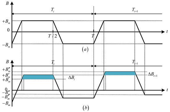
Figure 4.
The curves: (a) , . (b) , .
According to the definition of magnetic permeability :
where H represents the magnetic field intensity in the magnetic medium.
The current through the primary winding is the sum of secondary current converted to primary side and the magnetizing current :
where is the number of turns in the secondary winding.
The excitation current is measured under the no-load; therefore, is a relatively small current [26]. When is small, B increases with the increase of , and H is proportional to . However, when B increases to the saturation magnetic induction , it will not continue to increase, while H will continue to increase, according to Equation (7), and will decrease. Because is inversely proportional to , when begins to decrease, will begin to increase sharply. According to Equation (8), a large current pulse will be generated in due to the sharp increase of . When is greater than the rated current of the IGBT, IGBT may be damaged due to over current. The corresponding curves is shown in Figure 5.
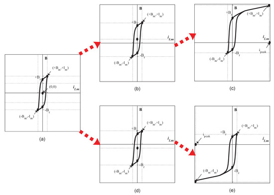
Figure 5.
The curves: (a) No DC Bias. (b) Positive DC Bias. (c) Positive Saturation. (d) Negative DC Bias. (e) Negative Saturation.
When the transformer is in steady state, the corresponding curve is symmetrical about the zero point , as shown in Figure 5a. However, if the transformer enters the positive DC bias state, the symmetry center will move up from the zero point, as shown in Figure 5b. And then, if the transformer enters the negative DC bias, the symmetry center will move downward from the zero point, as shown in Figure 5d. When the transformer enters the saturation state, the curve is distorted and no longer symmetrical, such as in Figure 5c, where the transformer enters the positive saturation state, and the curve is distorted in the first quadrant. Similarly, in Figure 5e, the transformer enters the negative saturation state, and the curve is distorted in the third quadrant.
2.2. Derivation of MIVVSPE
According to the above analysis, the current pulse produced in the primary winding is the result of transformer saturation, not the cause. In fact, the root cause of the transformer saturation is that the Integral Value of Volt-Second Product Error (IVVSPE) reaches and exceeds the Maximum Integral Value of Volt-Second Product Error (MIVVSPE).
Therefore, when the transformer enters the DC bias state, after N consecutive switching cycles, the Integral Value of Volt-Second Product Error can be expressed as:
When the transformer enters the positive critical saturation state, , if indicates that the transformer will enter the positive saturation state. On the contrary, when the transformer will enter the negative critical saturation state, , and, if , means that the transformer will enter the negative saturation state.
3. Proposed Suppression Strategy
To suppress the DC bias and prevent transformer from entering saturation state, a volt-second product error integral feedback control mode is proposed in this paper. Different from the traditional current feedback control mode in References [15,16,17,18,19,20,21,22,23,24], the trigger condition of this feedback control mode is the Integral Value of Volt-Second Product Error , and the DC bias suppression strategy can be triggered before transformer enters the saturation state. When , the positive DC bias suppression strategy will be triggered. When , the negative DC bias suppression strategy will be triggered. Therefore, the volt-second product error integral feedback control method proposed in this paper belongs to a active suppression method.
3.1. Construction of Closed-Loop Controller
According to the previous analysis, a closed-loop control structure from control variable (The duty cycle ) to feedback variable (The Integral Value of Volt-Second Product Error ) is constructed as shown in Figure 6.
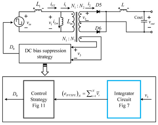
Figure 6.
The block diagram of closed-loop control structure with DC bias suppression strategy.
3.2. Synchronous Sampling and Integrator Circuit
In this control diagram, the key of the DC bias suppression strategy is the integral calculation of volt-second product error. Therefore, it is necessary to design an efficient and reliable long-time no zero drift integrator to measure the DC bias degree. The analog integrator has good dynamic response characteristics, but the zero drift of the integrated operational amplifier seriously restricts the application of the analog integrator in the long-time integration operation.
To solve this problem, a new long-time no zero drift integrator circuit is proposed in Figure 7. In the signal sampling part, the transformer in arc welding inverter is used to convert the high-frequency and high-voltage signal into a low-voltage small signal . In the part of integral operation circuit, the multi-thread parallel integral operation logic is constructed in the Field-Programmable Gate Array (FPGA) to improve the calculation speed of the , so as to ensure the real-time performance of the DC bias suppression strategy.
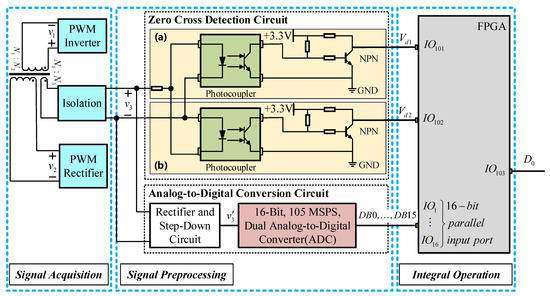
Figure 7.
Long-time no zero drift digital integrator circuit block diagram.
The long-time no zero drift digital integrator circuit is mainly composed of (1) Signal Acquisition Circuit, (2) Signal Pre-processing Circuit, and (3) Integral Operation Circuit. The main functions of each part are as follows:
- Signal Acquisition Circuit:The main function of this part is to sample the input voltage , where kHz, V. Considering that the main transformer in the arc welding inverter can be approximated to an ideal high precision voltage sensor. Therefore, a simple voltage detection method is proposed to realize the accurate synchronous sampling for the , in which an additional winding is wound on the main transformer core to convert into a low-voltage small signal , where V, . The actual waveforms are shown in Figure 8.
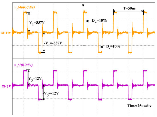 Figure 8. The waveforms of and .CH1 represents the input voltage waveform of the transformer, and the parameters of are: us, , V. CH3 represents the output voltage waveform of the additional winding, the parameters are: us, , V. Therefore, there is a very good relationship between the waveform and , so that the DC bias state, including the direction and depth, can be evaluated according to the change of .
 - Signal Pre-processing Circuit:The main function of this circuit is to preprocess the sampled signal to obtain the DC pulse square wave signals , and the 16-bit parallel signal .The Zero Cross Detection Circuit (a) is used to convert in the positive half-wave, and the duty cycle of the output voltage signal is equal to the positive half-wave of . Similarly, the Zero Cross Detection Circuit (b) is used to convert in the negative half-wave, and the duty cycle of the output voltage signal is equal to the negative half-wave of .Finally, the Analog-to-Digital Conversion (ADC) Circuit is to perform the analog-to-digital conversion on the amplitude of , the key parameters of the ADC module are shown in Table 1. Considering that the analog input range of the ADC module is 0∼ V p-p, it is necessary to rectify and step-down the input signal to get the DC pulse voltage waveform , and then perform the analog-to-digital conversion, where the output of the ADC module is a set of 16-bit parallel pulse sequences . The key waveforms are shown in Figure 9.
 Table 1. The main parameters of the high-speed parallel analog-to-digital converter (ADC).
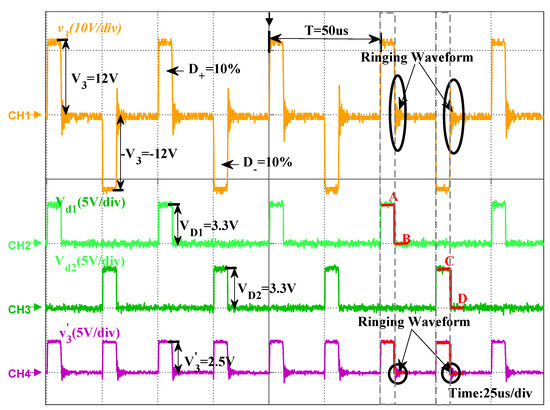 Figure 9. The key waveforms of the Signal Pre-processing Circuit.In Figure 9, CH1 is the waveform of the input voltage waveform , CH2 and CH3 represent the output voltage waveform and of the Zero Cross Detection Circuit (a) and (b), respectively, and CH4 represent the output voltage waveform of the Rectifier and Step-Down Circuit.
 - Integral Operation Circuit:The main function of this part is to calculate the integral value of volt-second product error. and is the output voltage of the Zero Cross Detection Circuit (a) and (b), respectively. While the 16-bit parallel input ports ∼ accepts the output of the ADC module. In order to improve the computing speed of , a parallel operation logic is constructed in FPGA, and the parallel thread structure diagram is shown in Figure 10.
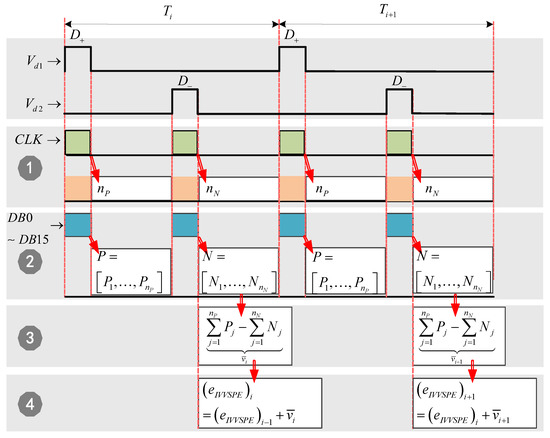 Figure 10. The structure diagram of the parallel operation for integral operation.The parallel operation logic is composed of 4 threads:
- Thread 1. Duty cycle counter:When the input variable or changes from Low to High, the 50 MHz counter starts counting, and then, if or changes from High to Low, the count result is assigned to or , the Thread 1 termination. Considering that the frequency of the counter is 50 MHz and the switching frequency is 20 kHz, so that and are a certain value, ranging from 0 to 2500. For example, in Figure 10, the duty cycle of positive and negative half-wave is ; therefore, the counting results of and is:
- Thread 2. Amplitude calculation:When or changes from Low to High, the Amplitude Calculation Thread begins to work, the amplitude of is calculated according to the output signals ∼ of ADC module. In the positive half-wave, the amplitude calculation result is stored in register , and then, in the negative half-wave, the amplitude calculation result is stored in register ,In addition, in the full-bridge DC-DC converter, when the IGBT switches from on state to off state, a Ringing Waveform will be generated in the output voltage waveform, as shown in Figure 9. However, the amplitude of the Ringing Waveform is relatively small and symmetrical about the zero axis; therefore, its influence on the calculation of the volt-second product error can be ignored. In Figure 7, the input threshold voltage of the Photocoupler in Figure 7 is about . Therefore, when , the output of the photocoupler is in the cut-off state, so that the Ringing Waveform in is filtered out. As shown in Figure 9, when IGBT is turned off, or will change from High to Low ( or ), at this point, both Thread 1 and Thread 2 are terminated.
- Thread 3. Volt-second product error calculation:When Thread 1 and Thread 2 are terminated, according to the definition of volt-second product error in Equation (3), the volt-second product error in the switching period can be calculated:Assume that the amplitude of in the positive and negative half waves is , then Equation (11) can be further written as:
- Thread 4. Integral of volt-second product error:According to the calculation result of volt-second product error in Thread 3 and the definition of integral of volt-second product error in Equation (9), the can be calculated:
3.3. Control Strategy
The block diagram of the control strategy for DC bias suppression strategy is shown in Figure 11.
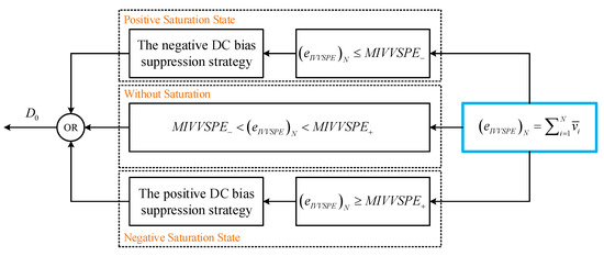
Figure 11.
The block diagram of the DC bias suppression strategy.
In Figure 11, the integral value of volt-second product error is used to evaluate the degree of DC bias, and the relationship between and DC bias degree can be defined as:
According to Equation (14), when the integral value of volt-second product error reaches and exceeds the Maximum Integral Value of Volt-Second Product Error or , the transformer enters the critical saturation state. In order to prevent transformer from entering the saturation state, the DC bias suppression strategy proposed in this paper will be triggered. The details are as follows:
- The positive DC bias suppression strategy.When , the transformer will enter the positive critical saturation state, in order to prevent the transformer from entering the positive saturation state, the positive DC bias suppression strategy is triggered, and the corresponding parallel thread sequence block diagram is shown in Figure 12.
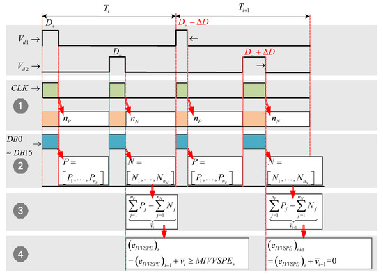 Figure 12. The block diagram of the parallel operation for positive DC bias suppression strategy.In Figure 12, the integral value of volt-second product error increases positively, due to the asymmetry of the circuit parameters in the full-bridge DC-DC converter, such as the gate drive signal, the turn-on/turn-off delay, and the on-resistance in of the IGBTs, so that . In order to reset quickly, and prevent the transformer from entering the positive saturation state, the duty cycle of in the switching period is adjusted, where the positive duty cycle decreases by , and the negative duty cycle increases by , ; therefore, , , so that the integral value of volt-second product error will be reset in the switching period :It should be noted that, when using duty cycle modulation technology to achieve DC bias suppression, large range step change of duty cycle within a switching period should be avoided, especially in one direction; otherwise, the transient dc bias will occur [23]. Therefore, in order to avoid this problem, the positive and negative half-wave duty cycle is adjusted by equal amplitude in reverse direction, as shown in Figure 12.
 - The negative DC bias suppression strategy.When , the transformer will enter the negative saturation state, in order to prevent the transformer from entering the negative saturation state, the negative DC bias suppression strategy is triggered, and the corresponding parallel thread sequence block diagram is shown in Figure 13.
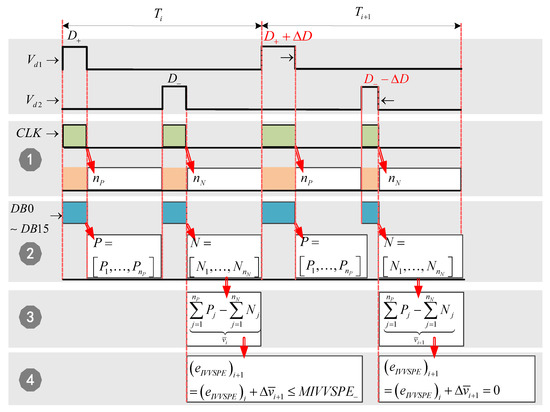 Figure 13. The block diagram of the parallel operation for negative DC bias suppression strategy.In Figure 13, the integral value of volt-second product error increases negatively, and . In order to reset quickly, and prevent transformer from entering the negative saturation state, the duty cycle of in the switching period is adjusted, where the positive duty cycle increases by , and the negative duty cycle decreases by , ; therefore, , , so that the integral value of volt-second product error is reset in the switching period :
3.4. Innovation and Advantages
The innovation is that the main transformer in the full-bridge DC-DC converter is used to measure high frequency and high voltage signal . Compared with the traditional Hall sensor measurement method, due to the magnetic core of the main transformer is large enough, the sampling method in Figure 7 has almost no signal distortion problem. Therefore, the signal sampling method proposed in this paper simplifies the circuit structure and improves the feedback accuracy.
The advantage is mainly reflected in the ability of the suppression strategy to restrain the saturation problem. Compared with the traditional current feedback control method, the suppression strategy can only be triggered after the transformer enters the saturation state. However, the volt-second product error integral feedback control method proposed in this paper will be triggered before saturation, which can completely eliminate the saturation problem.
4. Experimental Verification
In order to verify the DC bias suppression strategy proposed in this article, a 30 kW single-phase full-bridge DC-DC converter for the arc welding platform is established, as shown in Figure 14.
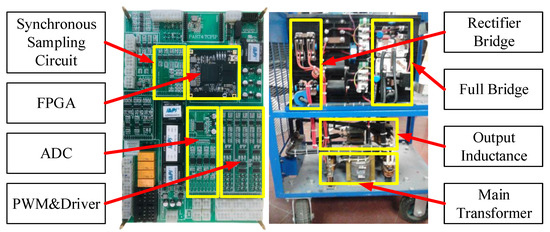
Figure 14.
Experiment platform.
The relevant parameters of the experiment platform are shown in Table 2. And three comparative experiments are given below, to illustrate the advantages of the proposed DC bias suppression strategy.
Table 2.
The main parameters of the arc welding platform.
4.1. No DC Bias Experiment
In this experiment, the full-bridge DC-DC converter is running in a steady state, and the primary input voltage is in a standard AC square wave, where , V. The key waveforms are shown in Figure 15.
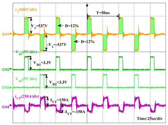
Figure 15.
The key waveform of inverter without DC bias.
CH1 represents the primary input voltage , CH2 and CH3 represents the output signals and , and CH4 is the current through the primary winding .
4.2. DC Bias Experiment
In practical application, the duty cycle asymmetry is one of the main reasons for the saturation fault of arc welding inverter. Therefore, to simulate this case, a duty cycle disturbance variable is introduced into the negative half-wave from the switching period , so that the negative half-wave duty cycle is increased to . The key waveforms are shown in Figure 16.
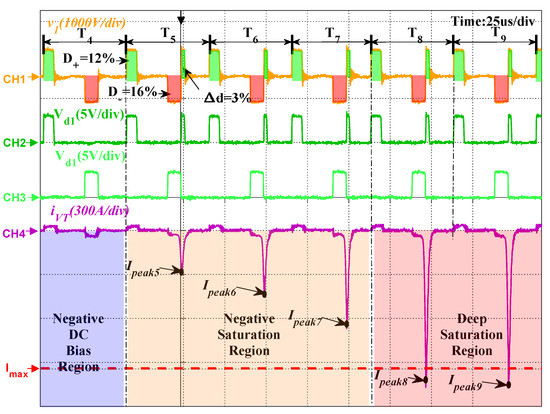
Figure 16.
The key waveform of negative DC bias.
In Figure 16, due to the introduction of , the volt-second product error accumulates in the negative direction, the transformer enters negative DC bias state, according to Equation (10):
Furthermore, according to Equations (12) and (17), the volt-second product error in the switching period can be calculated:
And then, according to Equations (9) and (18), the integral value of volt-second product error in the switching period is:
Since , . According to Equation (13) and the proposed DC bias suppression strategy, we can predict that the transformer will enter negative saturation state in , and a current pulse will be generated in the negative half-wave of and reach the maximum value at the moment . When , the switching period enters the negative half-wave continuous flow stage, with the rapid attenuation of , a reverse induction electromotive force with an equivalent duty cycle of will be induced in the transformer, where the induced electromotive force belongs to the positive pulse width. Therefore, the counting results of and in is:
Then, the volt-second product error in the switching period can be calculated:
Therefore, the actual integral value of volt-second product error in the switching period is:
4.3. DC Bias Suppression Experiment
In this experiment, compared with the traditional current feedback control mode, the volt-second product error integral feedback control mode is better in suppressing the DC bias and can completely eliminate the problem of transformer saturation.
- The traditional current feedback control mode.In the traditional current feedback control strategy, if the current peak caused by transformer saturation is greater than the preset reference current , the traditional DC bias suppression strategy is triggered, and then the duty cycle modulation method is used to correct the saturation state. The experimental results are shown in Figure 17.
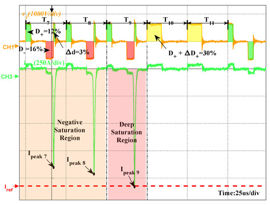 Figure 17. The experimental results of the traditional current feedback control method.In Figure 17, in order to compare the experimental results conveniently, the DC bias condition is the same as experiment 2, the transformer enters negative DC bias state, and when is greater than , the traditional DC bias suppression strategy is triggered, and then, in the next two switching cycles, the positive half-wave duty cycle increases to , while the negative duty cycle decreases to ; thus, the DC bias state is corrected.
 - The volt-second product error integral feedback control mode.Under the same DC bias condition as experiment 2, if the transformer enters the critical saturation state, the DC bias suppression strategy proposed in this paper is applied, and the experimental results are shown in Figure 18.
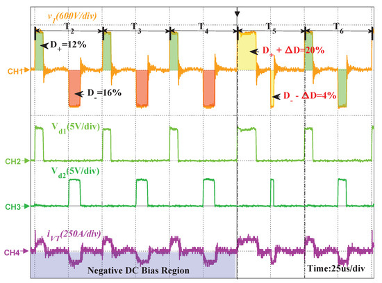 Figure 18. The experimental results of the volt-second product error integral feedback control mode.According to Equation (19), , the transformer enters the negative critical saturation state. In order to prevent the transformer from entering the saturation state, the negative DC bias suppression strategy proposed in this paper is implemented. Therefore, in the switching cycle , the duty cycle increment is:and then, in the switching period , the positive duty cycle increases to , while the negative duty cycle decreases to . According to the Figure 18, there is no pulse current in the waveform.
According to the experimental results in Figure 16, Figure 17 and Figure 18, under the same DC bias condition, the DC bias suppression strategy proposed in this paper can completely eliminate transformer saturation. Furthermore, when the DC bias suppression strategy is triggered, the adjustment mode and depth in duty cycle is based on the preset of or , while the size of and is determined by balancing the saturation risk and adjustment frequency. Therefore, the DC bias suppression strategy proposed in this paper has very good robustness in suppressing transformer saturation and can improve the anti-saturation ability of the single-phase full-bridge DC-DC converter.
5. Conclusions
A duty cycle modulation method for eliminating DC bias of single-phase full-bridge DC-DC converter is proposed in this paper. The magnetic saturation problem of transformer is effectively eliminated, and the operation stability of arc welding inverter is improved. Based on the detailed analysis of the saturation mechanism of transformer, the conditions for realizing zero DC bias and the closed-loop control model for adjusting the Maximum Integral Value of Volt-Second Product Error are given. In order to realize the integral operation of volt-second product error of transformer input voltage signal, a novel digital integration circuit with long-time no zero drift is proposed. When the Maximum Integral Value of Volt-Second Product Error reaches the trigger condition of the DC bias suppression strategy, the DC bias can be quickly corrected by adjusting the duty cycle of the H-bridge power switch drive signal. The experimental results verify the effectiveness of the method in preventing transformer saturation.
Author Contributions
Conceptualization, B.Q.; methodology, Y.Z. and B.Q.; software, Y.Z. and M.Z.; validation, Y.Z.; formal analysis, Y.Z.; investigation, Y.Z.; resources, B.Q.; data curation, Y.Z., B.Q., M.Z., and B.C.; writing–original draft preparation, Y.Z.; writing–review and editing, B.Q.; visualization, Y.Z.; supervision, B.Q. and B.C.; project administration, B.Q. All authors have read and agreed to the published version of the manuscript.
Funding
This work was supported by the National Natural Science Foundation of China (Grant No. U20B2031, Grant No. 52075024 and Grant No. 52075022).
Institutional Review Board Statement
All patients involved in this study gave their informed consent.
Informed Consent Statement
This paper has been approved for publication.
Data Availability Statement
The data provided in this paper are all true and effective, and have been repeatedly verified in experiments.
Conflicts of Interest
The authors declare no conflict of interest.
Abbreviations
The following abbreviations are used in this manuscript:
| MIVVSPE | Maximum Integral Value of Volt-Second Product Error |
| IGBT | Insulated Gate Bipolar Transistor |
| FPGA | Field-Programmable Gate Array |
References
- Paul, A.K. Power electronics help reduce diversity of arc welding process for optimal performance. In Proceedings of the 2010 Joint International Conference on Power Electronics, Drives and Energy Systems & 2010 Power India, New Delhi, India, 31 December 2010; pp. 1–7. [Google Scholar]
- Schupp, J.; Fischer, W.; Mecke, H. Welding arc control with power electronics. In Proceedings of the Eighth International Conference on Power Electronics and Variable Speed Drives, London, UK, 1 September 2000; pp. 443–450. [Google Scholar]
- Narula, S.; Singh, B.; Bhuvaneswari, G. Power Factor Corrected Welding Power Supply Using Modified Zeta Converter. IEEE J. Emerg. Sel. Top. Power Electron. 2016, 4, 617–625. [Google Scholar] [CrossRef]
- Paul, A.K. Simple means of resolving issues of AC-TIG welding equipment. In Proceedings of the 2016 IEEE International Conference on Power Electronics, Drives and Energy Systems (PEDES), Thiruvananthapuram, India, 14–17 December 2016; pp. 1–6. [Google Scholar]
- Mishima, T.; Nakaoka, M. A Novel High-Frequency Transformer-Linked Soft-Switching Half-Bridge DC–DC Converter With Constant-Frequency Asymmetrical PWM Scheme. IEEE Trans. Ind. Electron. 2009, 56, 2961–2969. [Google Scholar] [CrossRef]
- Tan, N.M.L.; Abe, T.; Akagi, H. Design and Performance of a Bidirectional Isolated DC–DC Converter for a Battery Energy Storage System. IEEE Trans. Power Electron. 2012, 27, 1237–1248. [Google Scholar] [CrossRef]
- Costinett, D.; Seltzer, D.; Maksimovic, D.; Zane, R. Inherent volt-second balancing of magnetic devices in zero-voltage switched power converters. In Proceedings of the 2013 Twenty-Eighth Annual IEEE Applied Power Electronics Conference and Exposition (APEC), Long Beach, CA, USA, 17–21 March 2013; pp. 9–15. [Google Scholar]
- Li, K.; Wang, Y.; Xu, J.; Wang, J.; Li, R.; Lv, C. A Novel Control Method for Eliminating DC Bias in Dual-Active-Bridge DC-DC Converters. In Proceedings of the 2018 IEEE International Power Electronics and Application Conference and Exposition (PEAC), Shenzhen, China, 4–7 November 2018; pp. 1–6. [Google Scholar]
- Jinhong, Z.; Wenlin, L.; Yaowu, S. Study on the dynamic process of arc welding inverter. In Proceedings of the IPEMC 2000. Third International Power Electronics Motion Control Conference (IEEE Cat. No. 00EX435), Beijing, China, 15–18 August 2000; pp. 308–311. [Google Scholar]
- Kwon, S.; Yoo, D.; Jeong, G.; Korea, S. High-Efficiency AC-DC Switch Mode Power Supply Using Full-Bridge Converter Circuit. Int. J. Control Autom. 2014, 7, 189–200. [Google Scholar] [CrossRef]
- Krismer, F.; Kolar, J.W. Accurate power loss model derivation of a high-current dual active bridge converter for an automotive application. IEEE Trans. Ind. Electron. 2009, 57, 881–891. [Google Scholar] [CrossRef]
- Zhao, B.; Zhao, B.; Song, Q.; Liu, W.; Zhao, Y. Transient DC bias and current impact effects of high-frequency-isolated bidirectional DC–DC converter in practice. IEEE Trans. Power Electron. 2015, 31, 3203–3216. [Google Scholar] [CrossRef]
- Mei, G.-H.; Liang, W.-J.; Liu, Y.-C.; Sun, Y.-Z.; Wang, D.; Mao, C.-X. Development of the DC current blocking device in capacitor-resistor for transformer. High Volt. Eng. 2009, 35, 2581–2585. [Google Scholar]
- Wang, Z.H.; Tong, X.; Qi, W.F. Blocking DC capacitor controllable opening and broken bridge suppression in transformer DC magnetic bias. Trans. China Electrotech. Soc. 2013, 28, 120–126. [Google Scholar]
- Hughes, A.; Drury, B. Electric Motors and Drives: Fundamentals, Types and Applications, 3rd ed.; Newnes: Burlington, VT, USA, 2005; p. 199. [Google Scholar]
- Gertsman, A.; Ben-Yaakov, S. Zeroing transformer’s DC current in resonant converters with no series capacitors. In Proceedings of the 2010 IEEE Energy Conversion Congress and Exposition, Atlanta, GA, USA, 12–16 September 2010; pp. 4028–4034. [Google Scholar]
- Baddipadiga, B.P.; Ferdowsi, M. Dual loop control for eliminating DC-bias in a DC-DC dual active bridge converter. In Proceedings of the 2014 International Conference on Renewable Energy Research and Application (ICRERA), Milwaukee, WI, USA, 19–22 October 2014; pp. 490–495. [Google Scholar]
- Dutta, S.; Bhattacharya, S. A method to measure the DC bias in high frequency isolation transformer of the dual active bridge DC to DC converter and its removal using current injection and PWM switching. In Proceedings of the 2014 IEEE Energy Conversion Congress and Exposition (ECCE), Pittsburgh, PA, USA, 14–18 September 2014; pp. 1134–1139. [Google Scholar]
- Takagi, K.; Fujita, H. Dynamic control and performance of a dual-active-bridge dc–dc converter. IEEE Trans. Power Electron. 2017, 33, 7858–7866. [Google Scholar] [CrossRef]
- Kohama, T.; Tokimatsu, S.; Shimamori, H. Elimination of magnetic saturation due to fast dynamic response in DC-DC converter. In Proceedings of the 31st International Telecommunications Energy Conference. Incheon, Incheon, Korea, 18–22 October 2009; pp. 1–6. [Google Scholar]
- Cho, J.-H.; Park, K.-B.; Park, J.-S.; Moon, G.-W.; Youn, M.-J. Design of a Digital Offset Compensator Eliminating Transformer Magnetizing Current Offset of a Phase-Shift Full-Bridge Converter. IEEE Trans. Power Electron. 2011, 27, 331–341. [Google Scholar] [CrossRef]
- Ribeiro, H.S.; Borges, B.V. Solving Technical Problems on the Full-Bridge Single-Stage PFCs. IEEE Trans. Ind. Electron. 2014, 61, 2264–2277. [Google Scholar] [CrossRef]
- Zhang, B.; Shao, S.; Chen, L.; Wu, X.; Zhang, J. Steady State and Transient DC Magnetic Flux Bias Suppression Methods for a Dual Active Bridge Converter. IEEE J. Emerg. Sel. Top. Power Electron. 2019. [Google Scholar] [CrossRef]
- Cuk, S.; Middlebrook, R.D. Advances in switched-mode power conversion part I. IEEE Trans. Ind. Electron. 1983, 1, 10–19. [Google Scholar] [CrossRef]
- Kazimierczuk, M.K. Full-Bridge PWM DC–DC Converter. In Pulse-Width Modulated DC-DC Power Converters; Publishing House: Wright State University: Dayton, OH, USA, 2015; p. 330. [Google Scholar]
- Heathcote, M.J.; Franklin, D.P. The J&P Transformer Book a Practical Tehnology of the Power Transformer Newnes; Butterworth-Heinemann: Great Britain, UK, 1998. [Google Scholar]
Publisher’s Note: MDPI stays neutral with regard to jurisdictional claims in published maps and institutional affiliations. |
© 2021 by the authors. Licensee MDPI, Basel, Switzerland. This article is an open access article distributed under the terms and conditions of the Creative Commons Attribution (CC BY) license (http://creativecommons.org/licenses/by/4.0/).