1. Introduction
Electric power systems have seen tremendous changes during recent years. One of the main reasons behind these changes is the huge diffusion of power electronics technology in electric power and energy systems. For example, to manage energy storage systems [
1], renewable energy sources [
2], to increase the performance of electric motor drives, electric vehicles [
3], in transportation systems [
4] and to give services to the mains or final user such as power quality services, energy management and demand response [
5,
6,
7,
8].
Therefore, it is essential to study the power converters’ behavior in detail aiming to design the best hardware and software solution able to improve their performance and efficiency. In this context, power electronics converter losses evaluation studies are becoming always more and more important.
For example, to reduce power electronics converters losses, zero voltage and zero current switching topologies have been developed and it is a topic of several research works e.g., in [
9] and [
10]. Some other studies proposed switching losses reduction and closed form solution to reduce conduction losses, in [
11] and [
12] respectively. Losses reduction in active power filters with a new pulse width modulation (PWM) strategy has been proposed in [
13]. The authors in [
14] and [
15] also aimed to design different power electronics devices with reduced losses.
Therefore, it is becoming essential to design power converter, not only selecting proper switching and heatsink devices according to power rating [
16], but also studying the behavior of each single component to evaluate its performance [
17]. As described in the IEC 62751 2 standard, which presents general principles, practical steps and recommendations for calculating the power losses in the converters and their switches [
18].
In this regard, it is fundamental to note that power electronics losses calculation is tied up with switches and components physical characteristics. Therefore, even if it is not possible to develop a generic model for losses calculation (because it is necessary to consider the selected components used in the power converter), it is possible to define a common approach which can be used for power electronics converters’ behavior and losses evaluation at their components level.
Considering this inescapable implementation limit, all the developed/proposed methods in literature have additional constraints. Indeed, these methods need extra time-consuming procedure which should be carried out in addition to the hardware and software design and development. Moreover, in most cases, it is very difficult to implement these methods into simulation tools and when the method permits this implementation, it is not possible to obtain a good power losses evaluation in a wide voltage and current operation range.
Therefore, an agile and handy new approach, able to evaluate, in a preliminary design phase, the power electronic converter losses with good accuracy and in a wide working operation range (covering wide range of current and voltage variations), is mandatory for designing better hardware and software (controller) solutions that could improve the performance of the power electronic converter.
This paper aims to fill in these gaps and solve these strong constraints adopting a new approach. Following this new approach, it is possible to evaluate power electronic converter losses of any hardware configuration and operating working condition, by simulation software tools, so it can reduce the extra efforts, the time spent on further analysis and/or the need to develop separate simulation models for loss evaluation.
To achieve this result, starting from the power losses evaluation methods available in the literature, new methods, that can cover a wide range of current and voltage variations, have been proposed. Comparison has been made to illustrate the better overall accuracy of proposed new methods over a wider operating range.
This new approach, gives the possibility to evaluate, unlike some available approaches in literature, the switching and conduction losses separately for each component, so the contribution of each power losses component to the total power losses can be discovered in the simulation environment during a preliminary design process.
Moreover, all methods are presented in a systematic way, so it is quite straight forward and easy for researchers to build their own models following the steps provided in the paper.
The rest of the paper is organized as follows:
Section 2 introduces the device losses.
Section 3 describes several methods (available basic method and the new methods) for power electronics switching losses evaluation, and
Section 4 does the same for conduction losses.
Section 5 describes the new approach introducing all the implementation steps that permits us to evaluate the total power electronics losses in a simulation environment.
Section 6 verifies the proposed methods adopted in this new approach and compares the results with Semikron SemiSel v4 online tool and
Section 7 points out the conclusion of the work.
2. Device Power and Energy Losses
The efficiency evaluation of a power electronic converter, even if it is fundamental for designing better hardware and software (controller) solutions, is always a very expensive activity (both in terms of time and resources) to conduct. Losses evaluation of a power electronic device and, in particular, of a semiconductor switch, can be performed adopting one of the following approaches [
19]:
Experimental tests. Adopting this approach, it is not possible to perform a converter losses evaluation in the preliminary design phase and it is possible to obtain only the total power electronic converter losses for a single (or limited number of) operation point with dedicated laboratory setup;
Physics-based simulations. A detailed physics-based simulation is mostly undertaken by finite element analysis which models the semiconductor switches in detail. This simulation method gives very precise and accurate results and matches very well with experiments, even if the simulation of a single switching cycle with a typical workstation may take one or a couple of days. Moreover, the simulation is mostly performed in open loop, so it is nearly impossible to perform losses analysis within the simulation model adopted to study a system or controller;
Behavior models. A behavior model is based on parameters and models provided by manufacturers, which also allows good losses analysis results (normally less accurate than physics-based simulations). These models can be used in simulation tools to simulate a power electronic converter (so, they can be a good trade-off between accuracy and simulation time), even if a complete losses analysis must be performed separately with respect to the design simulations;
Analytical (or mathematical) models. These models are very fast and simple, so they allow wide use implementation into simulation tools. However, usually they do not possess good accuracy and they cannot cover a wide operation range (of current and voltage).
Hence, it should be clear that the development of an accurate, complete, fast and simple approach, as a definitive solution for power electronic devices losses calculation, is becoming increasingly important.
Based on the above discussions, an analytical or mathematical approach is well suited to this contest because it can be adopted into simulation tools.
To develop analytical or mathematical power electronics losses calculation methods, simulation model-based approaches can be classified in two different categories:
The first one is to build a 3D look-up table from datasheet info and use it for dynamic losses calculation [
20,
21,
22];
The second is to approximate the losses with analytical formula and matching the formula with datasheet information by adjusting some coefficients [
16,
23,
24,
25,
26,
27,
28].
The first approach is very complicated to use and generally does not have good accuracy (unless a look up table is provided by manufacturer), because it is necessary to evaluate the losses directly by datasheet and in a small working operation range. The second one is preferable because it offers a systematic approach to study power converter losses and it is easy to implement even if it needs extra time to obtain good accuracy and adequate working operation range.
In the following, power electronics module losses are split up into three components namely:
The last component normally is negligible (comparing to switching and conduction losses) and its evaluation is also very difficult [
24]. Therefore, as normally happens in this kind of analysis, only switching and conduction losses are explained and modelled in the following
Section 3 and
Section 4.
It is important to note that in a real prototype, parasitic inductors and capacitances affect the voltage/current turn-on/off curves and consequently they can have effects on switching losses calculation [
19,
29]. Those parasitic effects are not considered in this study, because the focus of the paper is to propose an agile and simple new approach compromising the accuracy and computation burden (simulation speed and time). Therefore, the results are compared with similar studies. More accurate results are possible with more detailed modelling which needs more complex modelling and time-consuming simulations. Parasitic components’ effects can be considered as future studies.
Therefore, in the next sections switching losses and conduction losses methods are evaluated considering the datasheet info for the SEMIKRON “SKM400GB12T4” module (SEMIKRON, Nuremberg, Germany) with the nominal current of 400 A, the maximum collector-to-emitter voltage (VCES) of 1200 V (at Tj = 25 °C), and the switch operation temperature range between −40 °C to 175 °C.
3. Switching Losses Calculation and Modeling
Switching losses are present in a real switch during turning on and off intervals, because voltage and current waveforms do not perform a stepwise change, but have rising and falling shapes and slopes.
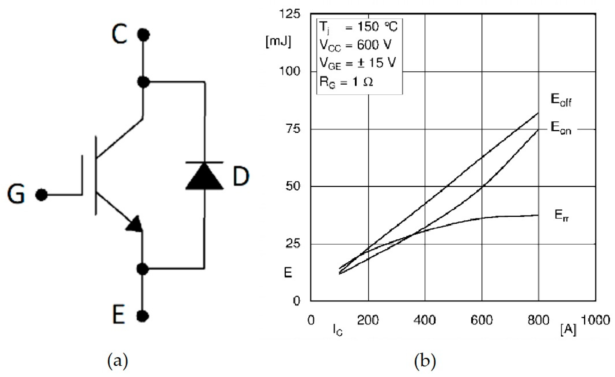
Considering the insulated-gate bipolar transistor (IGBT) with a freewheeling diode (FWD) module reported in
Figure 1a, it is possible to identify the following losses:
IGBT turn on energy losses (Eon);
IGBT turn off energy losses (Eoff);
FWD reverse recovery energy losses (Err).
Each power electronic module has its own manufacturing characteristics which defines its losses specifications. Therefore, for any power electronic device, extracting info from the manufacturer and the device datasheet is an unavoidable part in power electronics losses calculation.
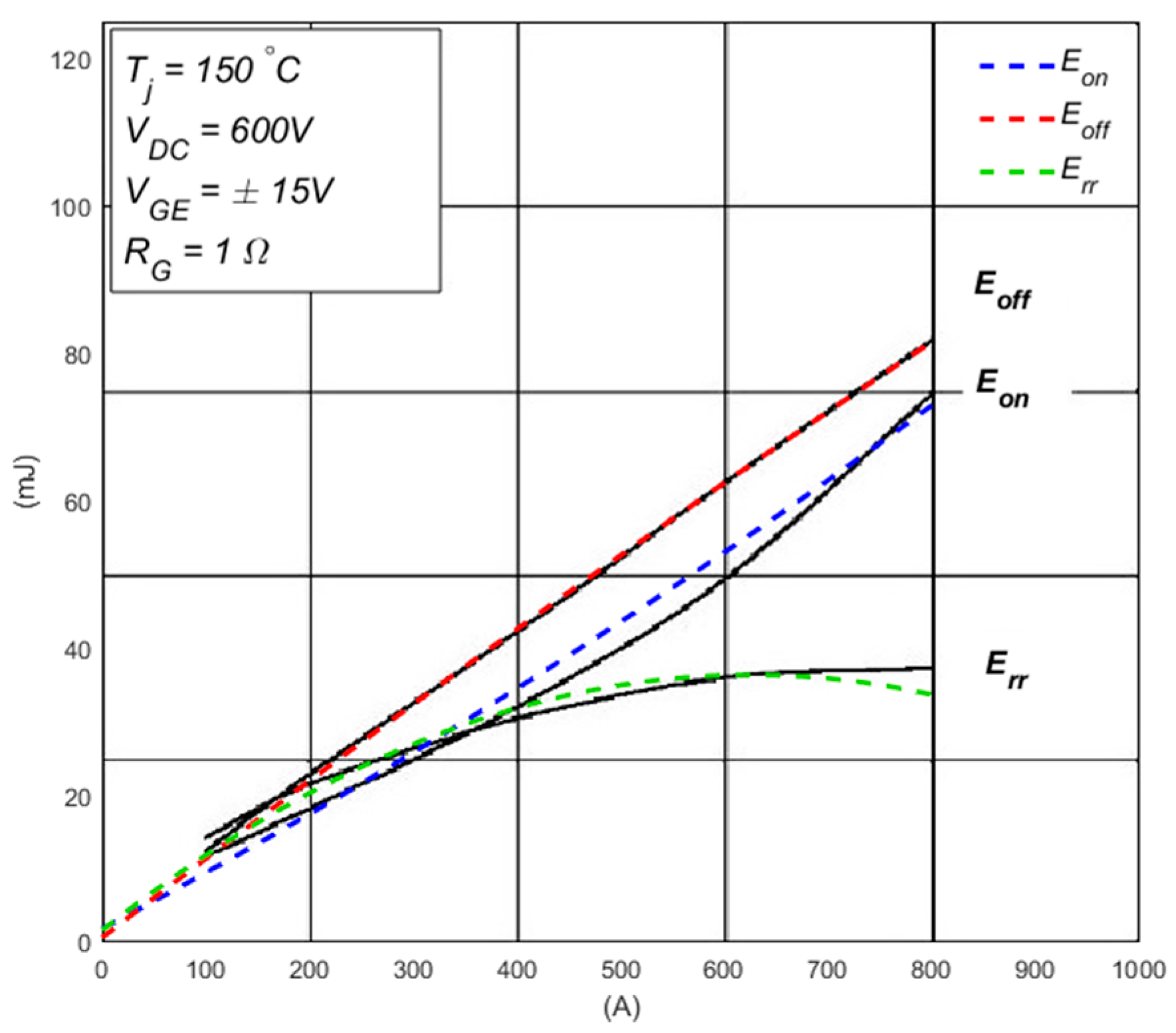
Usually, the datasheet reflects information about average energy losses of the module versus the operating collector current [
26] in three different graphs,
Eon for IGBT turn-on energy losses,
Eoff for IGBT turn-off energy losses and
Err for anti-parallel FWD reverse recovery energy losses, as in the example reported in
Figure 1b.
These graphs are realized by the manufacturer with experimental tests. They are obtained by measuring the instantaneous values of: collector current i, the supply (direct current (DC) bus) voltage vDC and junction temperature Tj (normally the last two parameters are constant in the experimental test so vDC = VDC,ref and Tj = Tj,ref) for a whole switching cycle. Then, the average of all the measures is reported in the graph to represent the switching energy losses of the device.
3.1. Method SW1
A typical analytical formula, described by Equation (1), allows a rough calculation of any energy losses effect [
27].
in particular, in Equation (1), the term
Esw1_T represents the IGBT turn-on (
Eon), or the IGBT turn-off (
Eoff) and the FWD reverse recovery (
Err) energy losses respectively.
In this way it is possible to represent the IGBT energy losses (Esw,IGBT = Eon + Eoff) and the FWD energy losses (Esw,FWD = Err) in function of the instantaneous values of: collector current i, supply (DC bus) voltage vDC and junction temperatures Tj.
Therefore, to use Equation (1) for IGBT and FWD energy losses, it is mandatory to identify:
Unfortunately, it is impossible to find the losses representation by Equation (1) in a wide range of working conditions. Indeed, Equation (1) gives a good losses approximation only when the real working condition of the power electronics is very close to the reference one, because the single exponents and coefficient values are evaluated close to the reference test condition only. Therefore, when the reference condition is close to the nominal one, it is possible to consider the exponents and coefficient suggested by manufacturers in their application note, as reported in the following [
27]:
Ki: exponent of current dependency (IGBT~1; FWD~0.5–0.6);
Kv: exponent of supply voltage (DC bus voltage) dependency (IGBT~1.2–1.4; FWD~0.6);
TCsw: temperature coefficient of switching losses (IGBT~0.003; FWD ~0.005–0.006).
Information in the device datasheet about energy losses of the module are mostly in function of the instantaneous or average current i or I value; instead, in some cases, it can be also observed that only two or three values for different voltage and for different temperature (always very close to their respective reference) are available. This is due because normally the DC bus voltage cannot change too much to avoid damaging the DC bus capacitors, and the junction temperature is controlled by means of heatsink and cooling systems (air or liquid cooling).
Therefore, considering
vDC =
VDC,ref and
Tj =
Tj,ref, it can be seen that the value of the exponent
Kv and coefficient
TCsw, do not have any effect on Equation (1). It can be simplified into the following:
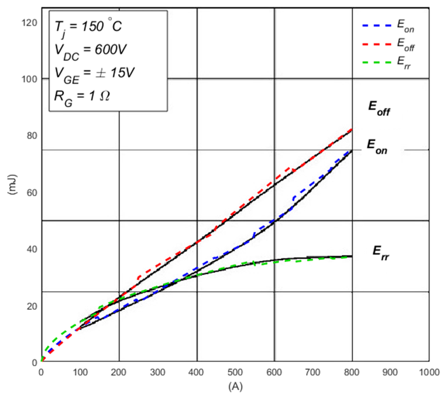
To understand the accuracy of this method, energy losses values are evaluated considering the datasheet info for the SEMIKRON “SKM400GB12T4” module. Using this device into the following working condition,
Irms = 400 A,
vDC = 600 V and nominal test temperature of
Tj = 150 °C, the reference
Esw,ref and exponents
Ki values, suggested by manufacturer in the application note, that can be used in Equation (2), are reported in
Table 1.
Using values reported in
Table 1,
Figure 2 compares the datasheet graphs of
Eon,
Eoff and
Err in solid black lines and their representation by Equation (2) in dashed colour lines.
From
Figure 2, it can be seen that Equation (2) can estimate the switching energy losses with quite good accuracy from about 200 A (50% of module nominal current) to about 600 A (150% of module nominal current) only. Therefore, in this simplified case, it can be observed that it is impossible to cover a wide range of current accuracy with a single exponent, so when this method is used in simulation tools using the instantaneous value of the current
i, it could give less accurate results. Moreover, when the working condition is far from the nominal one (e.g.,
vDC ≠
VDC,ref and/or
Tj ≠
Tj,ref) method SW1 cannot have a good accuracy.
3.2. Method SW2
When the real working condition of the power electronics is not close to the reference one, the losses representation by Equation (1) can still be used, even if the suggested value by the manufacturer in the application note for exponents Ki and Kv, and the coefficient TCsw cannot cover whole application range.
The new proposed method, for accurate losses modelling, divides the switching losses of the power electronic device in several small ranges.
As before, it is necessary to determine, the energy losses reference values Esw,ref, collector current reference value Iref, supply (DC bus) voltage reference value VDC,ref and junction temperatures reference value Tj,ref, that will be used for any range k.
After that to evaluate the correct parameters (for current, voltage and temperature), it is possible to use the following procedure for each range k.
By setting
vDC_k and
Tj_k to their reference values in Equation (1), it is possible to evaluate the current exponent
Ki_k, so Equation (1) can be rewritten as:
Using log function, Equation (3) can be linearized to find Ki_k values for both IGBT and FWD.
By setting
ik and
Tj_k to their reference values in Equation (1), it is possible to evaluate the voltage exponent
Kv_k, so Equation (1) can be rewritten as:
Once again, using log function, Equation (4) can be linearized to find Kv_k values for both IGBT and FWD.
In similar manner, by setting
ik and
vDC_k to their reference values in Equation (1), it is possible to evaluate the temperature coefficient
TCSW_k, so Equation (1) can be rewritten as:
Temperature coefficients can be found following similar procedure unless in this case, there is no need for linearization and the solution is straightforward.
As previously reported, it is not common to have wide variation of DC bus voltage (usually it is kept quite constant) and junction temperature (because it is controlled below a certain value by means of heatsink or cooling systems). Moreover, investigation reveals that switching losses have minor variation with respect to supply voltage (DC bus) change. Therefore, the suggested value in the application guide for voltage exponent Kv and temperature coefficient TCSW, can be used in all the defined intervals k. It is necessary to evaluate the correct exponent Ki_k for each selected range k, only.
Taking into consideration that to get a better accuracy it is better to consider the supply voltage and temperature variations, Equation (1) changes into the following:
In Equation (6) only Ki_k is function of the reference current ik used to represent the IGBT module, while the parameters Esw,ref, Iref, VDC,ref, Kv, TCsw, and Tj,ref are constant and equal to the reported values in the application note.
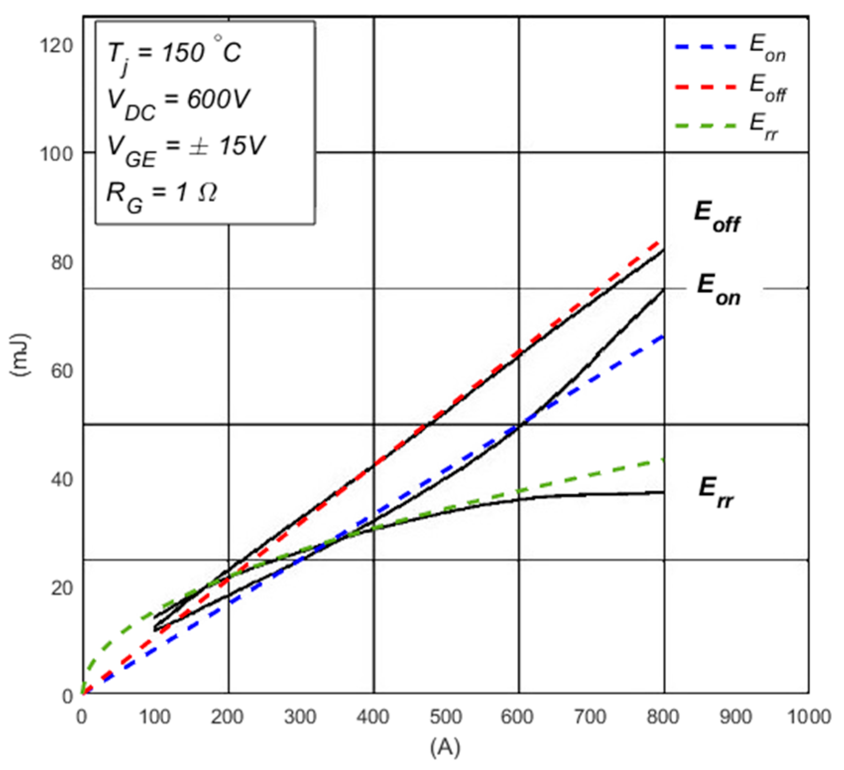
To understand the accuracy of this new method, the same IGBT module, “SKM400GB12T4”, is used. To represent the switching energy losses in any different range
k, the reference current
ik (extracted from the datasheet) and the best operating current exponents
Ki_k obtained by Equation (3) are reported in
Table 2.
It can be noticed that most of Ki_k exponents do not match the suggested values by the manufacturer unless close to the nominal current.
The other parameters adopted in this test are vDC = VDC,ref = 600 V and Tj = Tj,ref = 150 °C, and so the value of Kv and TCSW cannot affect the energy losses evaluation.
To verify the accuracy of the proposed method and considering these parameters,
Figure 3 reports the datasheet graphs of
Eon,
Eoff and
Err in solid black lines and their representation by Equation (6) in dashed colour lines.
It can be seen that with this new method Equation (6) can estimate the switching energy losses with good accuracy in a range wider than the method SW1, covering from about almost zero current up to about 800 A (200% module nominal current), so it can be used in simulation tools using the instantaneous value of the current i.
Obviously when the working condition is quite far from the nominal one (vDC ≠ VDC,ref and/or Tj ≠ Tj,ref), it is possible to evaluate the right exponent Kv and coefficient TCSW by using Equations (4) and (5) or using the average values suggested in the application guide of the exponent Kv and coefficient TCSW.
3.3. Method SW3
An interesting method, suggested by literature in [
16], is to use analytical second order polynomial formulas to represent the switching losses. Authors in [
16] illustrated that second order approximation is a good compromise between computation burden and accuracy, even if it is possible to match the switching losses curves more accurately by choosing high order approximation.
It is important to underline that in the switching losses evaluation in [
16], the supply voltage (DC bus) variation is considered linear (the voltage exponent is equal to one) and the temperature variation is ignored (junction temperature coefficient equal to zero). As reported in the datasheet supply voltage (
vDC) and temperature variations have a significant impact on losses evaluations when the device works far from its reference value. Therefore, to deal with these shortcomings, authors suggest using the following new method which is a combination of second order polynomial approximation and suggested formula by manufacturer.
The new completed method, which is a combination of second order polynomial approximation of [
16] and suggested formula by manufacturer, can be written as reported in Equation (7).
where
Esw3(
i) represents each switching energy losses
Eon(
i),
Eoff(
i) or
Err(
i), obtained by the generic analytical second order polynomial formula reported in Equation (8).
Second-order polynomial approximation can be done with Matlab curve fitting toolbox, MS Excel Trendline option or by measuring three different points from the losses datasheet curve around 25%, 100% and 175% of the nominal operating collector current value.
As for previous cases, the proposed model has a good accuracy using the exponent Kv and coefficient TCSW suggested in the application guide.
To understand the accuracy of this method, the switching losses are evaluated for the same IGBT module “SKM400GB12T4”. Here the Matlab curve fitting toolbox is used with the four points reported in
Table 3.
The starting point (0,0,0,0) is very important otherwise the losses could have high error when the collector instantaneous current i is close to zero.
Using the data reported in
Table 3 and Matlab curve fitting toolbox, it is possible to obtain the result reported in system (9).
As it is possible to observe in
Figure 4, system (9) fits quite well the datasheet info of the component, therefore, it can accurately represent the
Eon(
i),
Eoff(
i) and
Err(
i) at constant supply voltage and temperature in wide current application range so it can be used in simulation tools using the instantaneous value of the current
i.
It is important to underline that this new method can be used also when DC bus voltage and temperature are different to their reference value, indeed Equation (7) follows manufacturer’s suggestions updating the method [
16] representing the correlation between power losses and supply voltage (DC bus) and temperature variation.
3.4. Final Consideration
The use of the instantaneous current i to calculate switching losses allows a great flexibility in a simulation process. This permits to evaluate different control methods in transitory conditions, to evaluate the losses of each element during the design process, and so on. Using the instantaneous value of the current i, it is possible to evaluate the total power switching losses following each one of the described methods. Therefore, following the discussions in this section, method SW1 has limited current application range and owns lower accuracy, while both new methods, method SW2 and method SW3, have better accuracy for similar current range. Method SW2 is quite complicated to use in simulation software tools with respect to method SW3 because it is necessary to define several parameters with good accuracy (at least two values for each range).
In all the described methods, the parameters VDC,ref, Kv, TCsw and Tj,ref, which are necessary to describe each model, can be evaluated from the datasheet using the manufacturer’s suggested values.
Overall, it is possible to write that for switching losses evaluation, that needs instantaneous current values, it is very important to cover a wide current range, and in particular, it is very important to represent correctly the losses equation when the instantaneous current i is close to zero.
To evaluate the total power switching losses, it should be noted that the described methods calculate
Eon,
Eoff and
Err every switching cycle, but Equations (1), (6) or (7) are meant to estimate
Eon,
Eoff and
Err graphs reported by manufacturer and those are averaged values. Therefore, to evaluate the total power switching losses, it is necessary to make an average of evaluated
ESW over one switching cycle.
where Δ
t is the switching period and
fsw stands for switching frequency in hertz (Hz).
The total energy losses in one period is the sum of Eon, Eoff and Err energy losses. Moreover, the switching frequency must be considered to evaluate the total power switching losses.
Equation (11) represents the total power switching losses (
Psw) as the sum of IGBT power switching losses (
Psw,IGBT) and FWD switching losses (
Psw,FWD).
where
,
,
and
are described before and evaluated in Joule.
4. Conduction Losses Calculation and Modeling
Conduction losses on power electronics switching devices happens because during conduction period, switching devices do not behave as an ideal switch (zero on-state resistance and zero voltage drop). Indeed, they have on-state resistance and an amount of forward voltage drop on the device.
Usually the datasheet reflects information about conduction v-i characteristics of the module for IGBT and for anti-parallel FWD. These data are realized by the manufacturer running experimental tests at some temperatures Tj only (usually at max and min temperatures). Therefore, to evaluate the operational conduction power losses of the module, it is necessary to evaluate v-i characteristics and its dependency on the temperature. Therefore, also in this case a generic losses calculation model is not achievable, because each study must build its model considering the component in the power electronic converter.
Considering the same IGBT with the anti-parallel FWD module reported in
Figure 1a, it is possible to identify the following losses:
IGBT conduction power losses (Pcon,IGBT);
FWD conduction power losses (Pcon,FWD).
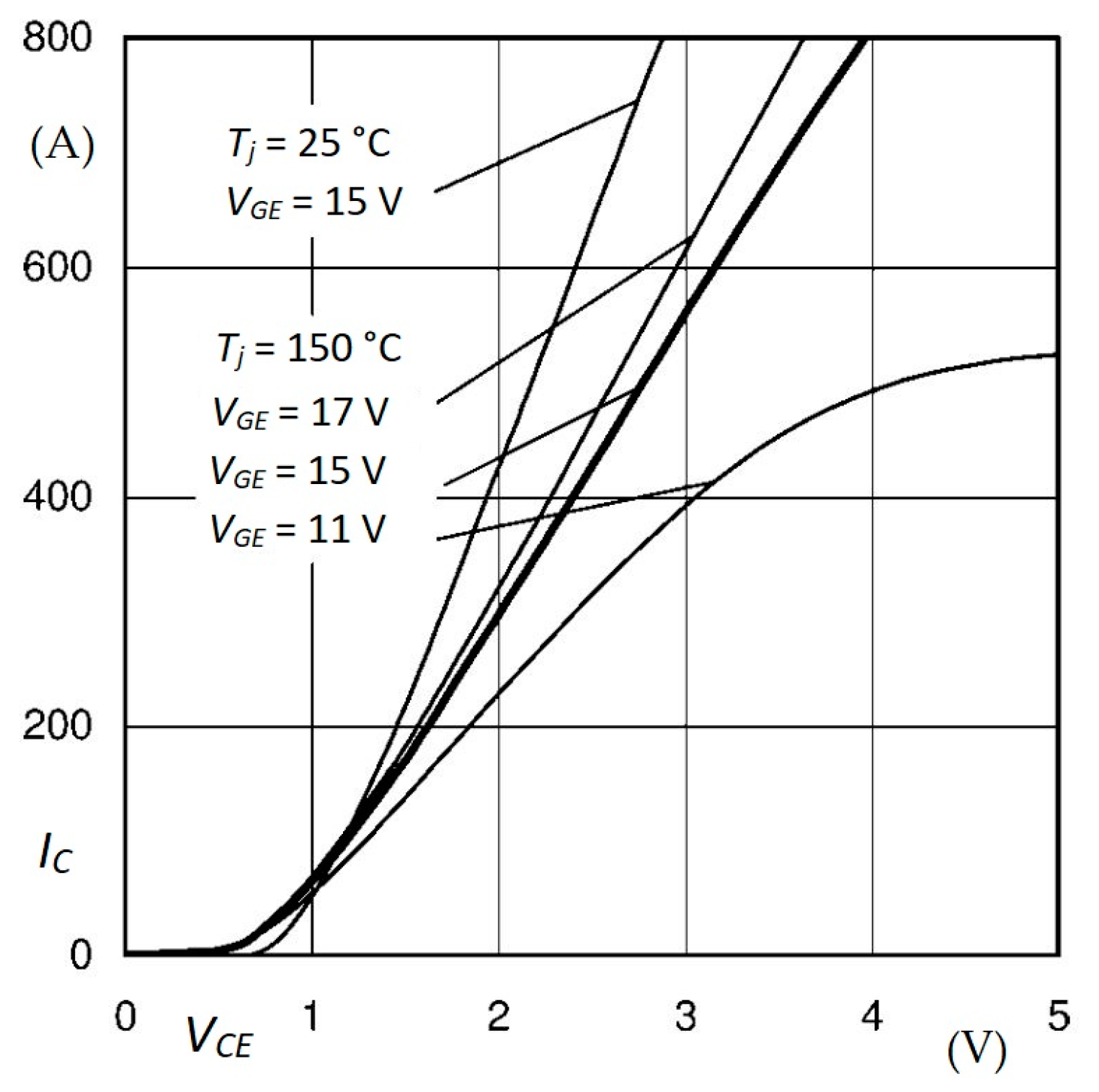
A typical curve of the
v-i characteristic of a semiconductor switch at a fixed junction temperature
Tj, is shown in
Figure 5 (extracted from datasheet).
Therefore, by extracting the switching characteristics (of IGBT and FWD) the conduction losses can be calculated using Equation (12), where the subscript
X has been used to represent IGBT and FWD because the formula is identical for both.
Normally, the datasheet provides v-i characteristic of the switch (IGBT or FWD) in a few points (two different temperatures Tmin and Tmax) and not in the whole working temperature range. Therefore, it is quite impossible to get accurate conduction losses evaluation in a function of time t, current i and junction temperature Tj, so Equation (12) cannot be used directly.
4.1. Method Con1
In
Figure 5, it is possible to see that the
v-i characteristic of the switch can be linearized with very good accuracy (when the gate-emitter voltage is high enough,
VGE ≥ 15 V, because as shown in
Figure 5, with low
VGE (=11 V) the
v-i characteristic misbehave), except the starting points where the level of current usually stays around few mA. Therefore, linear approximation for switch forward characteristics is considered and the
v-i curve can be linearized as:
where, the
RX(
Tj) is the on-state resistances (proportional to the gradient value) and the
VX(
Tj) is the voltage drops (proportional to the intercept value). Replacing Equation (13) into Equation (12) the instantaneous losses expression can be achieved.
The average conduction losses value in a period (2π) can be calculated by:
With simplification, the equation becomes:
where
IX and
iX,ave are the rms and average forward currents
iX through the switch.
Equation (16) reports the conduction losses at
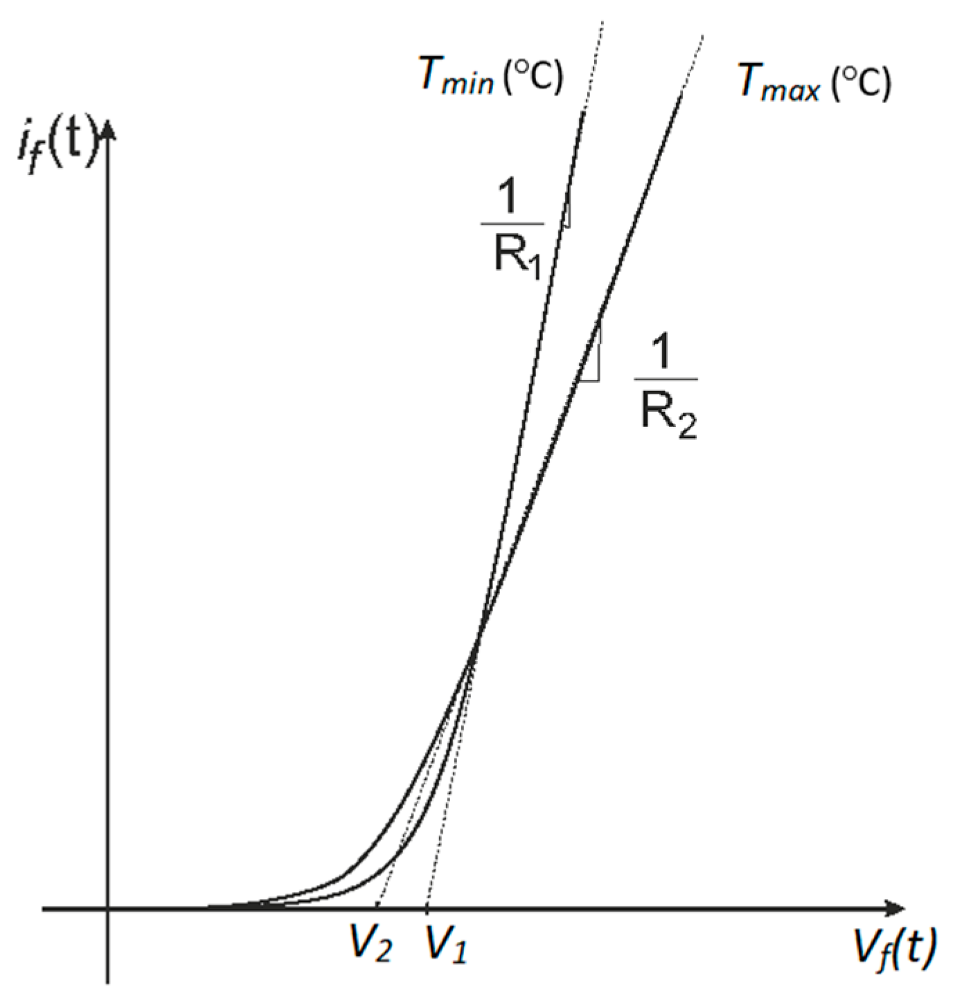
Tj junction temperature. It is imperative to consider the junction temperature variations but, usually datasheet provides
v-i characteristics of the switch (IGBT or FWD) in only two different temperatures
Tmin and
Tmax as it is shown in
Figure 6 where, as example, a typical forward characteristic of a diode and its linear approximation are shown.
Therefore, it can be quite easy to follow this procedure to evaluate conduction losses at these two temperatures but conduction losses value, at different junction temperature, is not achievable yet.
To solve this problem, the linear representation of the variation of resistances
RX and voltage drops
VX in function of junction temperature
Tj, can be represented by the first order (linear) functions that have a good accuracy and are widely used in literature as reported in [
16] and [
28]. These approximated correlations are reported in Equations (17) and (18).
In particular, Equation (17) represents the dynamic resistances of the switch and is the inverse slope of the v-i characteristic of the switch, while Equation (18) represents the voltage threshold which is where the switch starts conducting. These parameters depend on the junction temperature Tj, which means by increasing the junction temperature, the dynamic resistance increases while the threshold voltage decreases.
Extracting
Tmin,
Tmax,
R1(
Tmin),
R2(
Tmax),
V1(
Tmin) and
V2(
Tmax) from datasheet graph, the dynamic resistance and the voltage threshold relationships can be expressed by Equations (17) and (18) both for IGBT and FWD. Then the obtained results can be replaced in power conduction losses calculation Formula (16). Equation (19) reports the result.
To understand the simplicity and applicability of this method, in the following the conduction losses for the same IGBT module “SKM400GB12T4” have been evaluated. Therefore, its datasheet info has been used to find nominal (reference) values as reported in
Table 4.
These parameters can be used in the Equation (19) to evaluate the IGBT power conduction losses (
Pcon,IGBT) and the FWD conduction losses (
Pcon,FWD) respectively. Equation (20) represents the total power conduction losses (
Pcon) at any junction temperature
Tj and current
iX as the sum of these conduction losses.
This linearization method permits to evaluate power conduction losses in real working conditions in a very simple way because all the parameters can be simply determined. Normally it can be considered very accurate with a very good application range; however, linearization might not fit well to all applications especially where the v-i characteristic of the switch shows high non-linearity.
4.2. Method Con2
When the
v-i characteristic of the switch in real working condition shows high nonlinearity, as new proposal, the
v-i characteristic in
Figure 5, can be approximated by second order polynomial equation.
where the representation of
AX(
Tj),
BX(
Tj) and
CX(
Tj) need to be found. Here
Tj can be either
Tmin and
Tmax. This can be done, considering the two curves, of
Figure 6, reported in the datasheet at
Tmin and
Tmax, with Matlab curve fitting toolbox, MS Excel Trendline option or by measuring three different points for each
v-i characteristic curve of the datasheet.
In this work, the last approach is followed by obtaining the value of the v-i curve in the three points around 25%, 100% and 175% of the nominal current value from the datasheet.
Solving the linear system of three equations for the three unknown variables, it is possible to find the coefficients A1, A2, B1, B2, C1 and C2, where the subscripts 1 and 2 have been used, as in the example of the previous paragraph, for minimum and maximum junction temperatures respectively (Tmin and Tmax) that are not normal working conditions. Therefore, it is fundamentally important to find a strategy to obtain the right coefficient at the working junction temperature Tj.
As previously described, the same linear interpolation for resistant and voltage drop can be used to consider the temperature dynamics variation for the coefficients
AX(
Tj),
BX(
Tj) and
CX(
Tj).
Thanks to this new approximation, replacing Equation (21) into Equation (13), the instantaneous losses expression with second order approximation can be achieved.
The average conduction losses can be calculated by the following simplified expression.
where
i3X,ave is the average of cubed switch current.
To understand the method, the conduction losses of the same IGBT module “SKM400GB12T4”, has been considered. Starting from datasheet info of this device, the three points reported in
Table 5 for each curve has been used.
The obtained coefficients values are reported in
Table 6.
In this way, the power conduction losses of IGBT (
Pcon,IGBT) and FWD (
Pcon,FWD) with second order approximation method can be evaluated by Equation (24). Equation (25) represents the total power conduction losses (
Pcon) at any junction temperature
Tj and current
iX, as the sum of these two conduction losses for IGBT and FWD.
Second order approximation increases the complexity of the conduction losses calculation with respect to the previous method. Therefore, this new method is suggested when the v-i characteristic of the switch owns high non-linearity and/or the current ratio is low.
4.3. Final Consideration
The main problem in conduction losses evaluation is to formulate the v-i characteristic of the switch with an analytical equation. This can be done in several ways and it is the only difference between these two methods.
To evaluate the total power conduction losses, it should be noted that, normally the current that flow through the switching device, has high intermittency. Hence, the method Con1 seems to be a good compromise between simplicity and accuracy. Only when the device has a non-linear v-i characteristic and/or it is in low current conditions, new method Con2 is preferable.
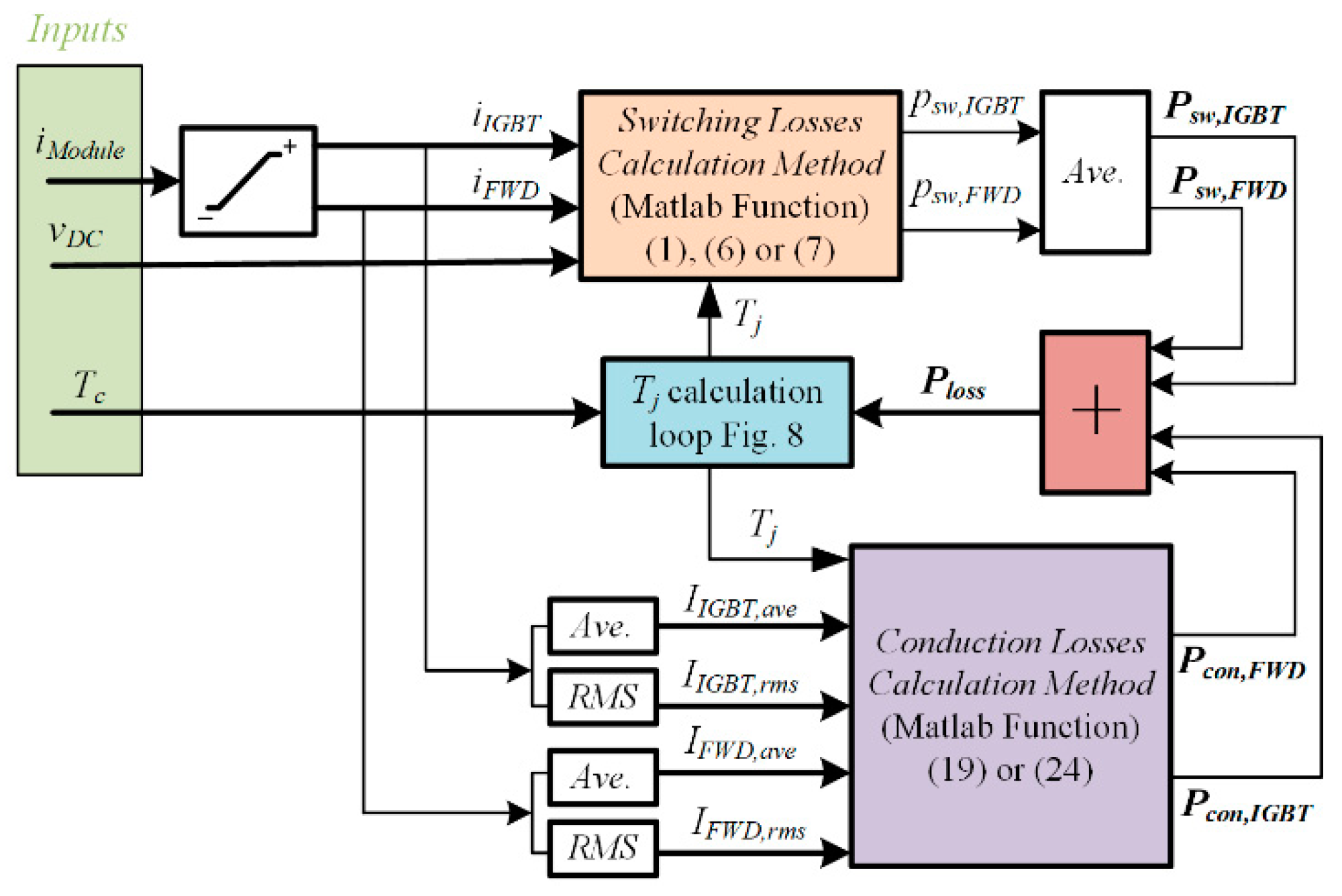
5. Total Losses Evaluation and Implementation Approach into Continuous Time-Domain
With equations described in
Section 3 and
Section 4, it is possible to calculate an IGBT with the anti-parallel FWD module power losses with good accuracy using the instantaneous value of the current
i or its derivatives. As reported in
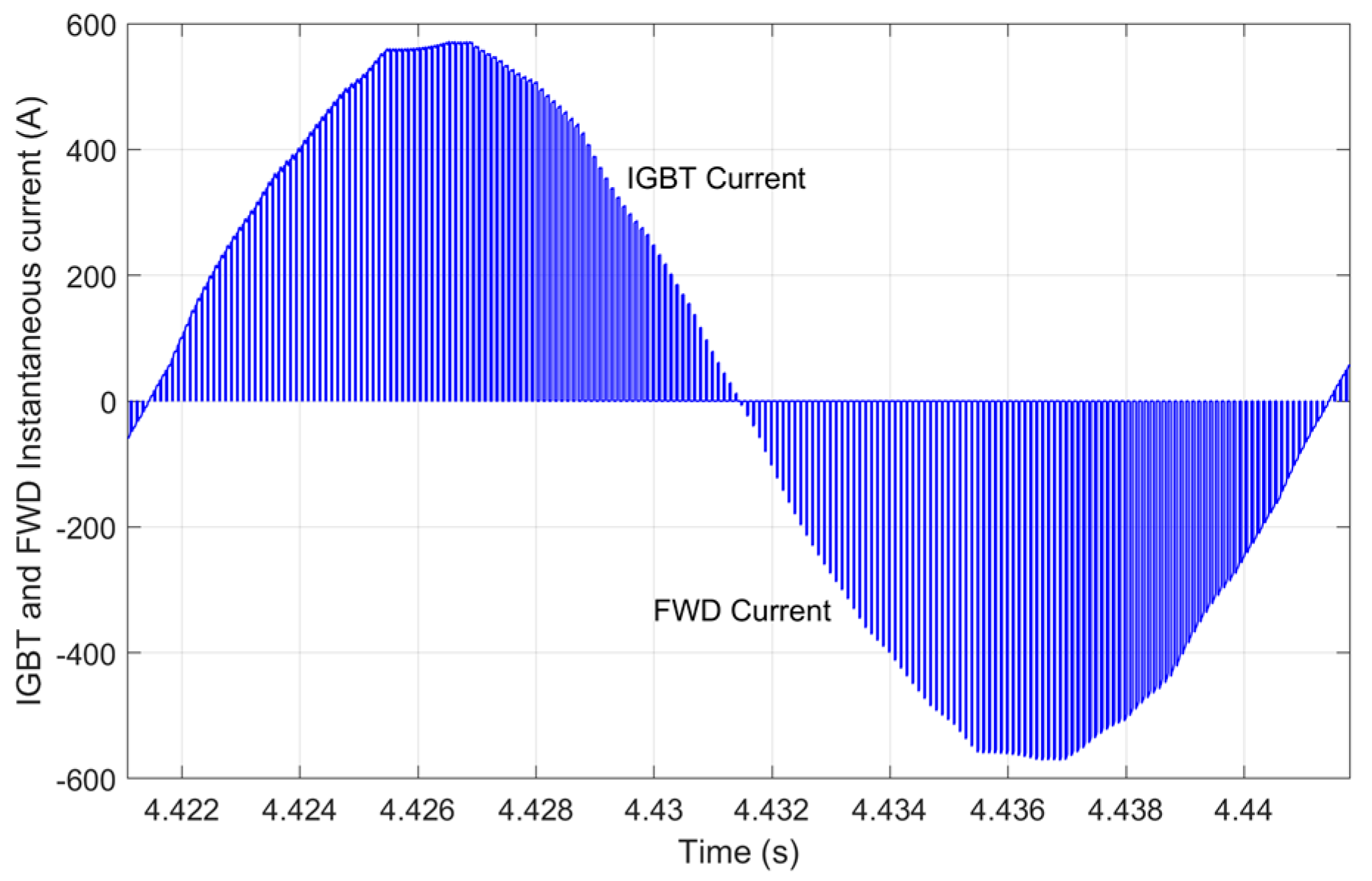
Figure 7, for rms load current equal to 400 A, the instantaneous current
i in semiconductor switch is varying between zero to around 150% of the rms load current.
Equation (26) represents the total power losses (
Ploss) as the sum of IGBT power losses (
Ploss,IGBT) and FWD losses (
Ploss,FWD) which consists of IGBT power switching losses (
Psw,IGBT), FWD switching losses (
Psw,FWD), IGBT power conduction losses (
Pcon,IGBT) and FWD conduction losses (
Pcon,FWD).
For switching losses evaluation, the required instantaneous measurements are: the collector-emitter current i, the module supply voltage (DC bus) vDC and the junction temperature Tj.
For conduction losses evaluation, the required measurements are: the collector-emitter current I and iave (rms and average current) and the junction temperature Tj.
All the voltages and currents measurements can be available in any simulation tool such as Matlab Simulink, the only missing part is the correct value of the working junction temperature
Tj of the device. It can be modelled inside the Matlab simulation with electro-thermal modelling [
22] as well, but it needs detail info about the design and implementation of the power electronics converter.
To have a better accuracy in power losses estimation, the temperature behaviours of IGBT and FWD need to be considered. The working junction temperature Tj can be evaluated by the thermal junction to case (j-c) resistances, for IGBT Rth_IGBT(j-c) and for FWD Rth_FWD(j-c).
These values are reported in the datasheet. Then knowing the ambient temperature (
Ta) it is possible to estimate IGBT and FWD working junction temperature by the following equation [
30].
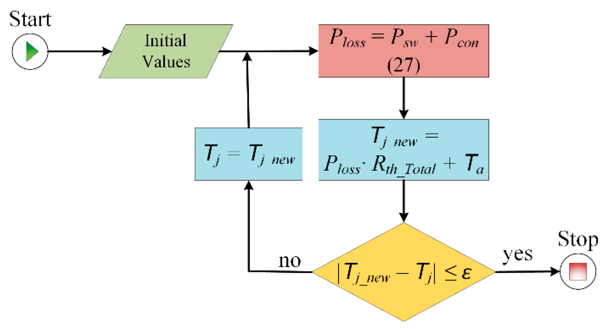
This equation does not consider the heatsink or cooling system where power electronic switches are installed. The heatsink design and characteristics can be modelled and included in the temperature evaluation process. The cooling system, can be natural air cooling, forced air cooling (fans) or a liquid cooling system, also it can be modelled as a thermal resistance and included in Equation (27), depending on configuration in series or parallel to the junction to case resistances. The temperature estimation depends on several design factors and it is out of the focus of this paper. However, upon availability of all data, the implementation in this model, to include temperature variation, can be undertaken as depicted in
Figure 8.
Initially Tj is considered equal to ambient temperature, Ta. Ploss is calculated and then based on the Ploss, the new junction temperature can be estimated. Then the absolute value of the temperature variation is checked, when it is within acceptable error (e.g., Ɛ = 1 °C) the losses calculation can be terminated, otherwise the new junction temperature Tj_new is considered as Tj and a new Ploss is calculated again.
All presented loss calculation methods can be implemented in any simulation environment following the implementation approach explained here.
In a simulation environment, all the instantaneous current and voltage signals, of any power electronic module, can be measured. In particular, as it is depicted in
Figure 9, it is possible to separate IGBT and FWD instantaneous currents in a simple manner, because the positive current flows through IGBT, while the negative current flows through FWD.
Switching losses calculation methods, need instantaneous values, so current, voltage and temperature values are used to evaluate instantaneous switching losses (psw,IGBT and psw,FWD) for IGBT and FWD. Considering that datasheet reports averaged values (energy losses curves), these values are averaged over one switching cycle to obtain the switching losses, Psw,IGBT and Psw,FWD.
Indeed, conduction losses methods calculation need rms current, average current, and temperature values. Therefore, IGBT and FWD currents rms and average values and temperature are used to obtain Pcon,IGBT and Pcon,FWD.
6. Results Comparison—Models Versus Semisel
To compare different losses evaluation methods, it is mandatory to define a reference point. Data coming from manufactures, such as datasheet information (utilized so far), is the most reliable one because manufacturers have done series of experimental tests on their products and collected all the required information.
Laboratory experimental test results are affected by additional parameters such as parasitic components. Moreover, it would be very difficult to separate switching and conduction losses for IGBT and FWD in a single module (usually only total losses can be evaluated). Therefore, instead of laboratory experimental test results, the Semikron SemiSel online tool has been used as benchmark in this study.
Semikron has the SemiSel v4 online simulation tool for different purposes [
31]. After selecting one of the few predefined hardware configurations and inserting the device parameters, it is possible to select the semiconductor switching module (among available Semikron products). Then the tool gives operational information including the power losses. SemiSel v4 gives power losses in separated form, reporting for any single device switching and conduction losses (
Psw,IGBT and
Pcon,IGBT for IGBT and
Psw,FWD and
Pcon,FWD for FWD) and the total losses of the converter under analysis (
Plosses).
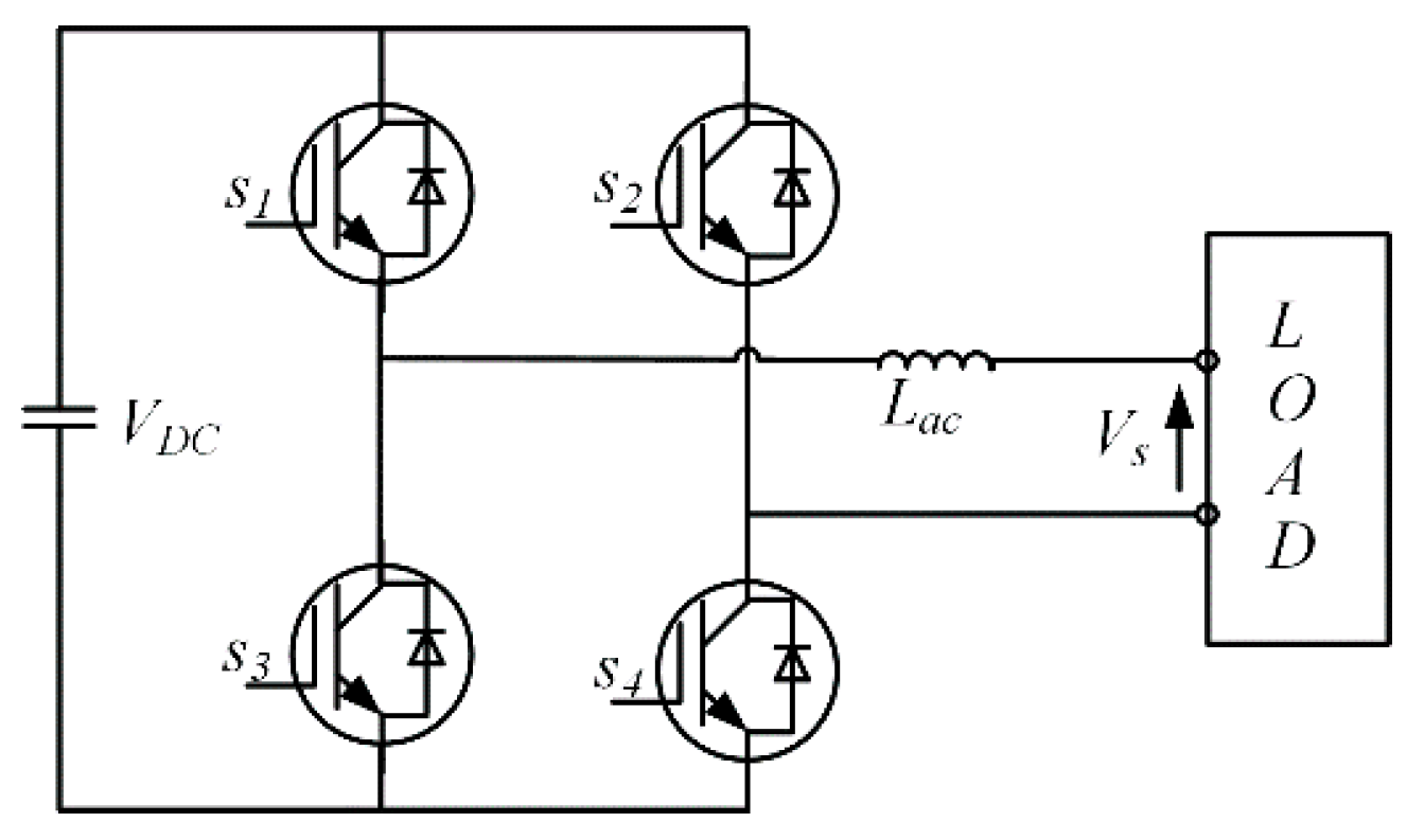
To compare each losses calculation method of this study to the reference one, a single-phase DC to AC inverter model is used to evaluate and compare the results. The test circuit is shown in
Figure 10. The inverter is controlled, at switching frequency of 5 kHz, as AC voltage generator (
Vs) to supply at 230 V/50 Hz, four different loads, with a load power factor of 0.9.
The losses are evaluated with three different DC bus voltages.
Following the implementation approach into the simulation tool described, it is possible to observe that in this test circuit, there is not a variation of the DC voltage (
vDC =
VDC), therefore, in the losses calculation it has been treated as constant value. Moreover, the junction temperature can be obtained depending on working condition following the new procedure described in
Figure 8 or fixing it at the beginning of the simulation process to the estimated value given by the Semisel tool. To simplify the simulation process in this paper, the junction temperature was considered as a known parameter.
Table 7 reports the four test conditions (A–D) and the working junction temperature
Tj used.
The same IGBT module “SKM400GB12T4” is always used as switching component to realize the single-phase DC to AC inverter. Then, it was used in a wide range (low current and over current) of working conditions.
6.1. Switching Losses
In this section IGBT switching losses (Psw,IGBT) and the FWD switching losses (Psw,FWD) have been reported and compared versus Semisel results.
Table 8 reports the results for the four different loading conditions described in
Table 7 when the DC bus voltage fixed to 500 V.
Table 9 and
Table 10 repeat the same loading steps with DC bus voltage fixed to 600 V and 700 V, respectively.
It can be noticed that method SW1, originally suggested by manufacturer, is associated with high error sometimes even more than 50% specially calculating FWD switching losses.
It should be noted that the value in the last row in
Table 8,
Table 9 and
Table 10 (same for
Table 11,
Table 12 and
Table 13) is the average error of all four selected working conditions which is meant to show the overall improvement of the losses evaluation accuracy. A deeper look into reported results reveals that the error falls below 5% in some cases specially when the current is close to the nominal one. Instead, the associated error is quite high in other working conditions (sometime more than 100%), especially when the current is quite low or rather high.
In general, it is a challenging task to calculate or estimate switching losses, and results reveal that it is much more difficult in the case of FWD rather than IGBT. Method SW2 has better accuracy even if the accuracy has been improved further utilizing method SW3 which proposes a second order polynomial approximation. In these cases, method SW3 has losses evaluation error less than 20% and in some cases around 10%.
It should be noticed that proposed losses calculation methods are evaluated in wide range current.
6.2. Conduction Losses
In this section IGBT conduction losses (Pcon,IGBT) and FWD conduction losses (Pcon,FWD) have been reported and compared versus Semisel results.
Table 11,
Table 12 and
Table 13 report the results for the same four different loading conditions when the DC bus voltage is fixed to 500 V, 600 V and 700 V respectively.
Conduction losses estimation both for IGBT and FWD has good accuracy with both Con1 and Con2 methods even if, in the analyzed cases, method Con1 has better accuracy with respect to method Con2. Only in some cases, method Con2 leads to a better accuracy with respect to the other one.
Considering the linear v-i characteristic, it is easy to understand the reasons why method Con1 outperforms method Con2. Method Con2 uses the cubed of switch current as it is reported in Equation (23), therefore it cannot perfectly fit the linear behavior of this device at high current values as method Con1 can do.
In general, it can be noticed that in this case the associated error is lower compared to the switching losses calculation errors, this is due because the current variation during the conduction period is very low.
Therefore, the best practice could be to use the linear (first order) approximation method and avoid complexity which may increase the calculation error somehow. This might not be the case for all other switches.
7. Conclusions
To increase the losses calculation accuracy, the paper describes a new approach introducing some new methods for switching and conduction losses calculation of IGBT with FWD module that can be used during simulations. Moreover, unlike the common methods in the literature, this paper evaluates and compares the switching and conduction losses separately for both IGBT and FWD.
For switching losses calculation, considering reported tests in the paper, new completed method SW3 showed a very good compromise between complexity, computation burden and accuracy with respect to other described methods. However, it is important to underline that only the new method SW2 can fit very well the energy losses curves reported in the datasheet. Therefore, only method SW2 should be used to cover a very extended range of currents.
For conduction losses calculation, method Con1 is associated with lower error to estimate IGBT and FWD conduction losses. Method Con2 led to better accuracy in some cases but worsens the losses calculation accuracy in some other cases. Therefore, for conduction losses calculation, method Con1 can be considered the better method to be adopted unless the v-i characteristic of the device possesses high non-linearity and/or the current is low.
Therefore, combination of method SW3 for switching losses and method Con1 for conduction losses performs better to calculate the overall losses of the device and it is easily applicable in all the simulation processes.
The new proposed approach is discussed in a more generic way, so it can be easily used in simulation tools with other switching devices. Moreover, considering that it can be used for any current, voltage, temperature, control strategy, switching frequency and hardware configuration, it can be considered more useful with respect to the Semisel online tool v4. Since Semisel has only some popular configurations, such as a single-phase DC-AC inverter, three-phase DC-AC inverter, direct converter and two types of three level inverters.
To increase the accuracy of the models, manufacturers should provide more numerical information on switching energy losses (Eon, Eoff and Err) and also on-state resistance RX and voltage drop VX at different temperatures Tj beside energy losses graphs and components v-i characteristic curves.
For future studies, the presented methods can be further developed to consider parasitic components’ effects in switching losses evaluation. Moreover, with detail thermal modelling, the junction temperature evaluation can be improved, and it will increase the accuracy of the results. As another direction for future study, the converter heatsink or cooling system can be considered in thermal modelling for temperature evaluation, which can be useful for final converter design.


