Article

Functionalized Three-Dimensional Multilayer Ceramic Modules

1
Institute of Micro- and Nanotechnologies MacroNano®, Electronics Technology Group, Ilmenau University of Technology, 98693 Ilmenau, Germany
2
Micro Systems Engineering GmbH an MST Company, 95180 Berg, Germany
*
Author to whom correspondence should be addressed.
Electronics 2021, 10(3), 248; https://doi.org/10.3390/electronics10030248
Submission received: 31 October 2020 / Revised: 7 January 2021 / Accepted: 13 January 2021 / Published: 22 January 2021
(This article belongs to the Special Issue LTCC for Space, Imaging, Telecommunication, and Medical Applications)

Abstract

:
Three-dimensional interconnect devices are still strongly related to plastic materials. Since the use of these materials is limited in harsh environments, there is an application gap, which could be filled by ceramic circuit carriers. Low-temperature cofired ceramics (LTCC) offer promising solutions to fill this gap. This work provides a feasibility study, including the whole technological chain of ceramic multilayer processing. Targeting a curved multilayer substrate, fully equipped with SMD (Surface-mounted device) components, the particularities of single process steps are investigated. Two shaping methods based on quartz glass molds are compared with regard to shape fidelity and technological effort. The investigation of internal conductor lines and via connections reveals that the metallization should have a minimum width of 200 µm and the via diameter is limited to 150 µm. Further considerations focus on the possible footprint of components and use of cavities to increase the footprint of components. The limits of wire bonding on curved surfaces were inspected. Finally, the work presents a demonstrator of a fully equipped four-layer ceramic circuit, including internal wiring. Hence, the transfer of the 2.5-dimensional multilayer ceramic technology into the third dimension is proven.

1. Introduction

The first ideas for functional three-dimensional multilayer circuits based on low-temperature cofired ceramics (LTCC) technology were described at the beginning of the 1990s [1]. Later, in 2004, a research team reported the possibility of producing three-dimensional structures out of a laminated LTCC stack by using tools to bend the substrates between an angle of 20 degrees up to 80 degrees. The surface of the curved structure was metallized and soldering pads were attached [2,3]. These investigations demonstrate the requirements for deformation of LTCC containing printed conductors. Further work on forming or rolling LTCC stacks followed between 2005 and 2013 [4,5,6,7,8,9,10]. The works of [4,9] contain rolled LTCC substrates with functionalized metallization on the inner or outer surface, and [9] describes the use of two different metal pastes. These two different pastes were used to produce heater and sensor structures. Both the inner and the outer structures contain soldering pads for connection on the same side as the structure. There was no necessity for the use of vias so far.
All these research works show the flexibility of non-metallized and metallized LTCC substrates. A further step in the production of complex, fully functionalized three-dimensional LTCC substrates is now the insertion of vias for connecting the individual layers and the investigation of their behavior in curved substrates.
The vision of the present work is to produce a three-dimensional (cylindrical) fully functional LTCC substrate with vias, inner and outer conductor lines and a component assembly on the top. It describes the production of an LTCC multilayer substrate with vertical connections (vias) in four iteration steps, based on the state of the art of metallized, bended multilayer substrates without vias.
The innovation is the production and examination of bended four-layer LTCC substrates in which the individual layers are connected electrically to one another by vias. So far, no research results demonstrate such complex ceramic multilayer modules.
Studying the behavior of vias during bending is preceded by a substrate production without any vias or metallization in order to achieve safe handling in this field. Subsequently, the influence of elongation and compression on metallization caused by bending is examined. This is followed by the analysis of the weakening influence (diameter and distance to one another) of the vias to the substrate during bending. This is one of the last missing steps in order to transfer the two-dimensional LTCC technology into the third dimension. We recommend process conditions which allow the further processing of bended LTCC substrates containing via connections and metallized interconnections with a yield of 95%. A fully functional, three-dimensional LTCC substrate with vias, inner and outer interconnections and a completely assembled surface is presented as a final demonstrator.

2. Experimental Procedure

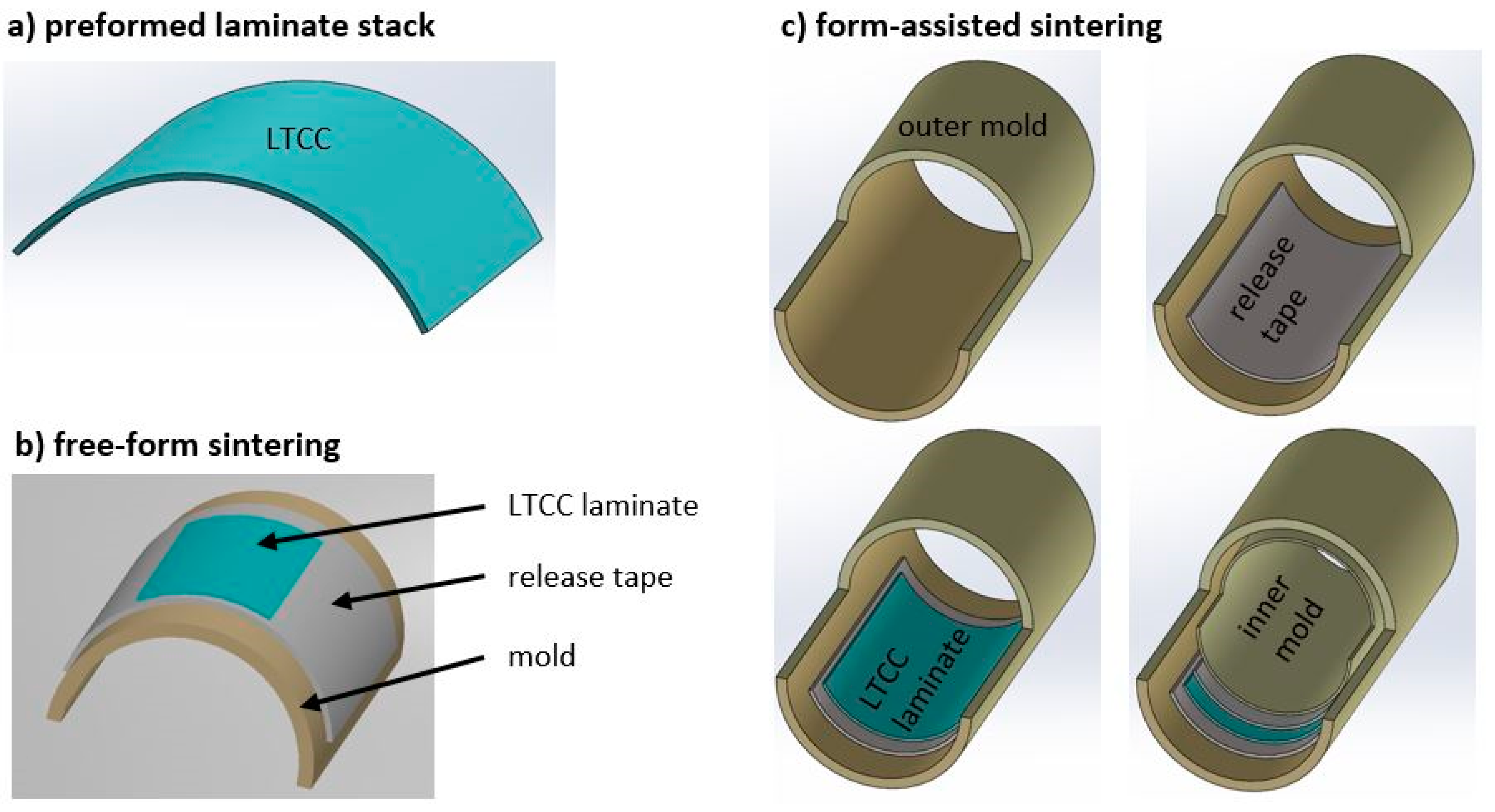
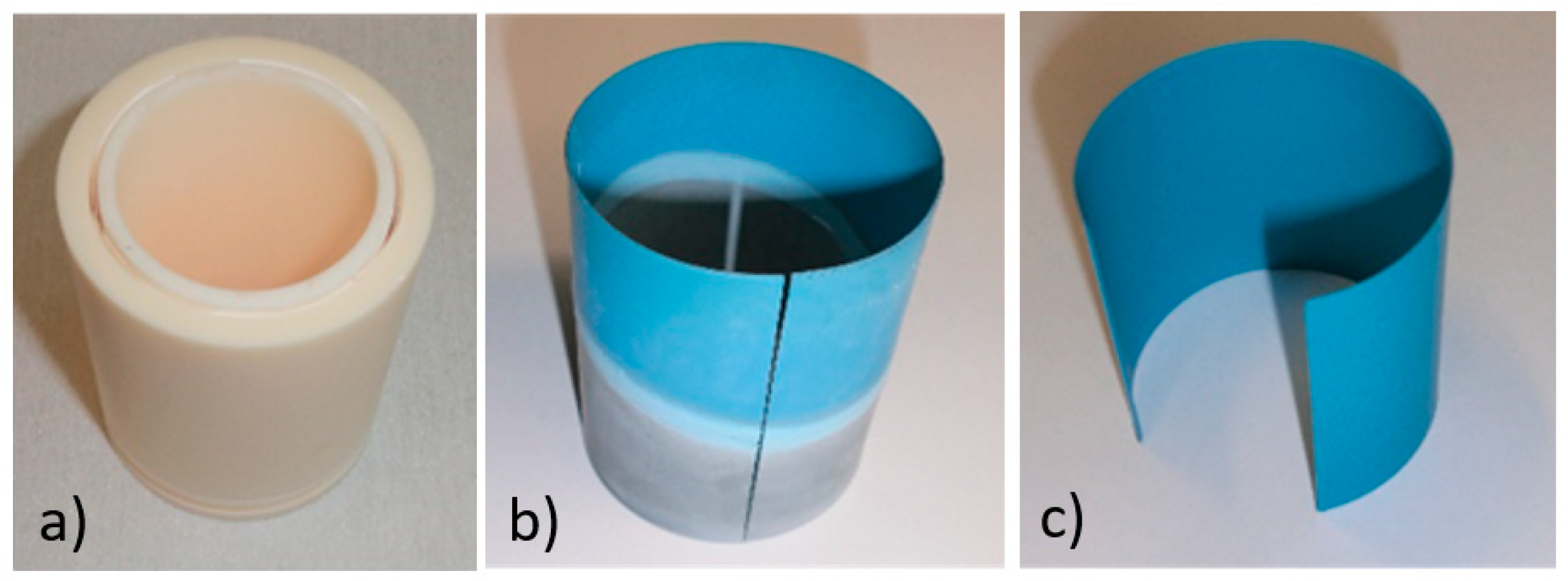
2.1. Technological Approach

The targeted radius r of the current application is 22.5 mm. The length of the multilayer substrate l amounts to 46.5 mm and the width w is 21.5 mm. The complex layout requires the reliable connection of surface components by means of inner wiring and surface conductors, including vertical contacts (vias) and landing pads for bonding and soldering. To investigate the behavior of such complex LTCC substrates under bending, a five-stage test plan was applied. It allows the assessment of critical dimensions and derivation of appropriate design rules at different technological levels. The complexity of the substrate structure increases from the first to the fourth stage corresponding to the technological levels 1–5 shown in Table 1. Level 5 combines all necessary structures in the final layout of the multilayer circuit.
All substrates consisted of 4 layers DP 951 PX Green TapeTM (DuPont de Nemours, Wilmington, DE, USA). The green sheets were stacked and isostatic laminated with a pressure of 200 bar at a temperature of 70 °C. The initial sinter profile increased the temperature in one hour from 400 °C to 500 °C for debindering and held the sinter temperature of 875 °C for 30 min. A multipurpose fast ramping furnace (PEO 603, ATV GmbH, Vaterstetten, Germany) was used. The conventional process chain of cutting, via punching, screen printing, stacking, laminating and sintering changed after the lamination process. Figure 1 illustrates the modified handling. The laminate had to be pre-formed to fit on or in the respective mold. The mold was a quartz glass tube with the targeted radius. Alumina tape (Ceramtec®A, CeramTec GmbH, Eberbach, Germany) was used as the so-called release tape. The alumina densified at much higher temperatures than the used LTCC tape. Therefore, the alumina remained in powder state and prevented sticking of the LTCC material on the quartz glass mold. All the utensils required for shaping, including the base plate, quartz form and release tape, were heated for about 10 min at 80 °C in a drying oven with forced convection (Binder GmbH, Tuttlingen, Germany). It was necessary to bend the laminate manually to fit into the mold. It was placed on the warmed quartz glass, separated by one layer of release tape.
Depending on the position of the laminate, shown in Figure 1a, we distinguished two sintering methods: free-form sintering (Figure 1b) and form-assisted sintering (Figure 1c). In the case of free-form sintering, the laminate was placed on the outer diameter of the mold. The metallization on top of the substrate was stretched. Form-assisted sintering used the inner diameter of the mold, and the metallization on top of the substrate was compressed. A second inner mold with a matching diameter was necessary to prevent curling. It was inserted on a second layer of the release tape. The whole assembly was placed in the sinter furnace. In the case of free-form sintering, the mold was positioned horizontally in the oven. Using form-assisted sintering, the whole assembly was placed vertically in the sinter furnace.
The criteria to compare the two different methods of shaping an LTCC substrate were the necessary complexity of the mold, the need to change standard technology, preparation effort and the dimensional accuracy of the sintered substrate.
At the first technological level, we investigated the sinter conditions. The shape was evaluated, as described in Section 2.2. Section 3.1 summarizes the results.
The effects of the bending on surface metallization were assessed at the second technological level. Table 1 summarizes the used silver and gold pastes. All conductor tracks were printed on a screen printer (EKRA M2, EKRA Kraft GmbH, Bönnigheim, Germany) using a stainless steel screen VA 400° × 0.018° × 22.5° coated with Murakami photopolymer MS15. Figure 2a shows the test layout. The fired thickness of all considered conductor structures was between 7 µm and 9 µm.
The conductor width varied between 70 µm and 200 µm. The printing direction was along the circumference of the multilayer cylinder as depicted in Figure 2b. Ten substrates were processed in the experiment. The structure repeated four times on the substrate. The shaping was performed using both methods, free-form sintering and form-assisted sintering. After firing, the metallization was evaluated with an optical microscope and the functionality of the conductor lines was tested with a multimeter (Agilent 34401A Digital Multimeter, Agilent Technologies, Incorporated, Loveland, CO, USA) in order to identify electrical disruptions. Section 3.2 presents the results.
Technological level three contained the inner conductor tracks and vias. The line width of the conductors varied between 75 µm and 175 µm and the spaces varied between 75 µm and 300 µm. Two vias connected the inner layers and allowed the electrical testing according to Section 2.3. As can be seen from Table 1, only a silver paste was used for conductor lines in these tests. A via test field contained structures with different diameters and densities. The diameter was 50 µm, 75 µm, 100 µm, 150 µm and 200 µm. These diameters were punched with different pitches; the vias had no electrical contact, defects were evaluated only optically. All results are given in Section 3.2.
The effect of the whole design complexity was investigated at technological level 4. Daisy chains containing vias and conductor paths on all four layers served as test structures. Different layouts were used, and the respective test structures were aligned along the circumference and in perpendicular direction as well. The investigation after sintering used X-ray imaging (Nanomex 180 + CT, X-ray Service GmbH, Premstätten, Austria) and electrical measurements. Figure 3 depicts X-ray images demonstrating the layout of two different daisy chain layouts used in this work.
The full integration level includes, finally, the assembly of surface components. Section 3.3 explains details of the process.

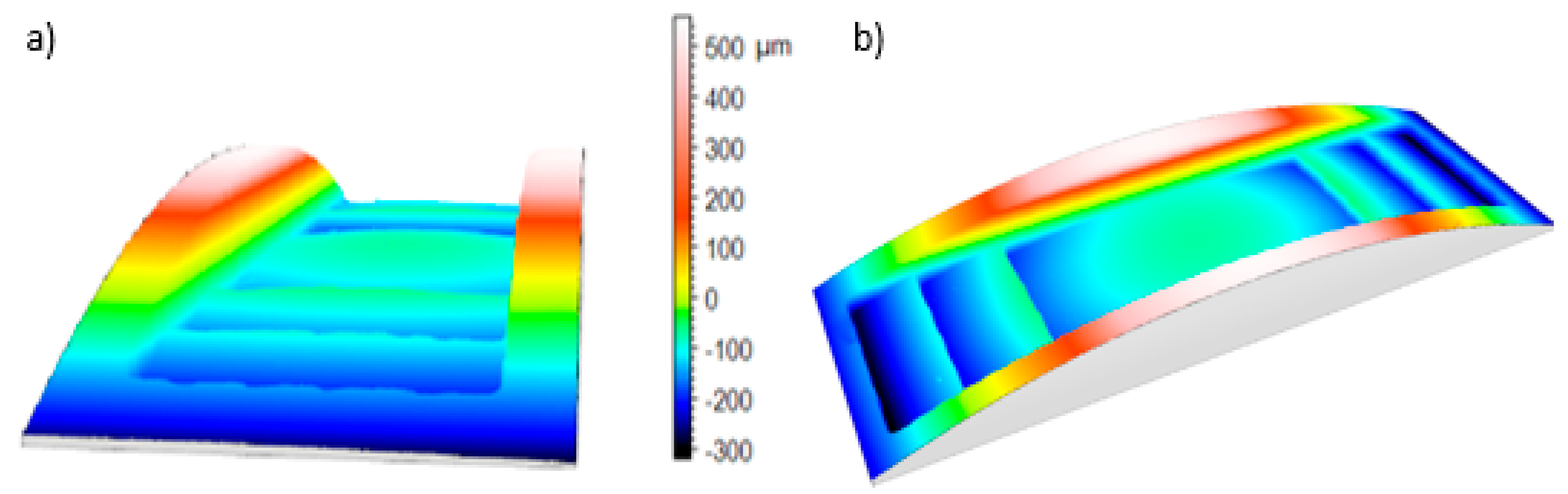
2.2. Shape Measurement

The exact determination of the target radius r = 22.5 mm after sintering was conducted with the Faro Arm Fusion laser scanning system (Faro Arm Fusion, FARO Europe GmbH & Co. KG, Korntal-Münchingen, Germany). The measurement was carried out by means of optical scanning, and the accuracy amounted to ±35 µm. This value is suitable for evaluation of the shape fidelity in our experiment. The used measurement method was based on a comparison of the theoretical design draft with the measured result. The measurement with the Faro Arm was an optical scanning of the substrate and the matching software provided a three-dimensional image of the measured object. The comparison of the scan data with the theoretical design results is the depicted deviation in Figure 4. This deviation provides information about the manufacturing accuracy and shape fidelity of the substrate.

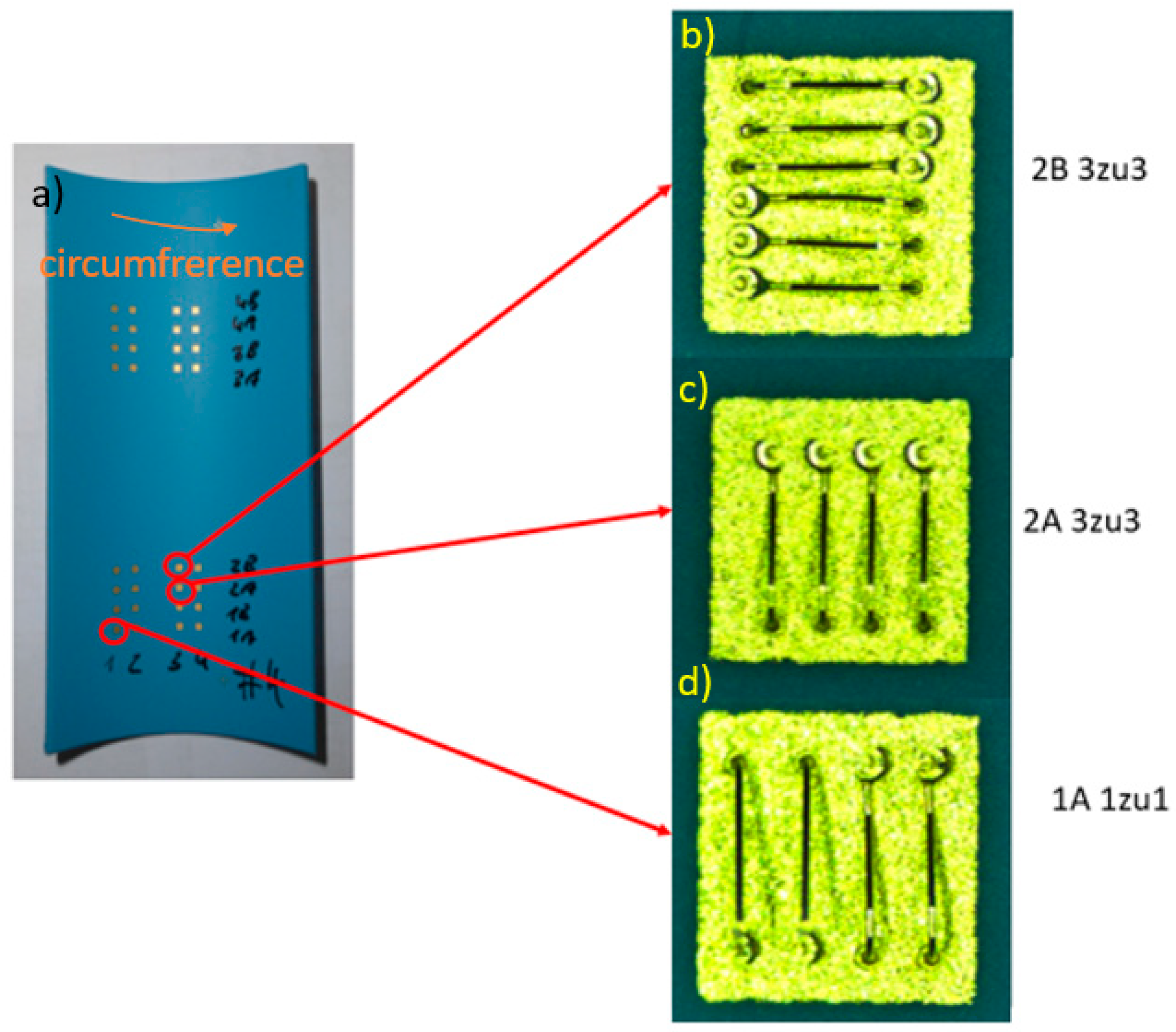
2.3. Adaption for the Assembly with Components

Wire bonding on curved surfaces is a particular challenge because the thermal contact differs from even substrates and surface pressure varies in addition because of the surface shape.
In order to obtain a tight thermal contact, an adapted substrate holder made of aluminum as shown in Figure 5 was used. This substrate holder can easily be heated on the device’s own heating plate and thus guarantees a stable bonding temperature.
Wire bonding (ball wedge) was investigated as a possible interconnection technology for components on the curved LTCC circuit carrier. Bond tests were carried out on inner and outer surfaces with minimal adjustment of the wire bonder (Bonder Delvotec 5410, F&K Delvotec Bondtechnik GmbH, Ottobrunn, Germany). The bond connections were produced at 130 °C with the parameters shown in Table 2.
Due to the radius of 22.5 mm and the fact that chip and SMD mounting cannot level tolerances larger than 100 µm, the size of components which can be placed on the curved LTCC surface was limited to approximately 4 mm × 4 mm in their footprint dimensions.
The assembly of components with larger footprint requires the creation of planar plateaus. Cavities provide a solution for this problem. Three layers built the cavity, whereby the length of the cavity differs from layer to layer, while the width remains constant. After bending, this created a surface with an evenness in the range of 100 µm. Images taken with the laser scanning microscope (LSM LEXT OLS 4100 Olympus, OLYMPUS EUROPA SE & Co. KG, Hamburg, Germany) depict the height profile of a representative cavity in Figure 6. The view along the cavity in Figure 6a illustrates the height difference between the outer radius and the bottom of the cavity. It amounts to approximately 700 µm. The perspective view in Figure 6b points out that the height tolerance at the bottom of the cavity is in the range of 100 µm and can be equalized by typical underfills. Since the surface tolerance is a function of the layer thickness, it is possible to achieve even closer tolerances when the layer thickness is reduced.

3. Results and Discussion

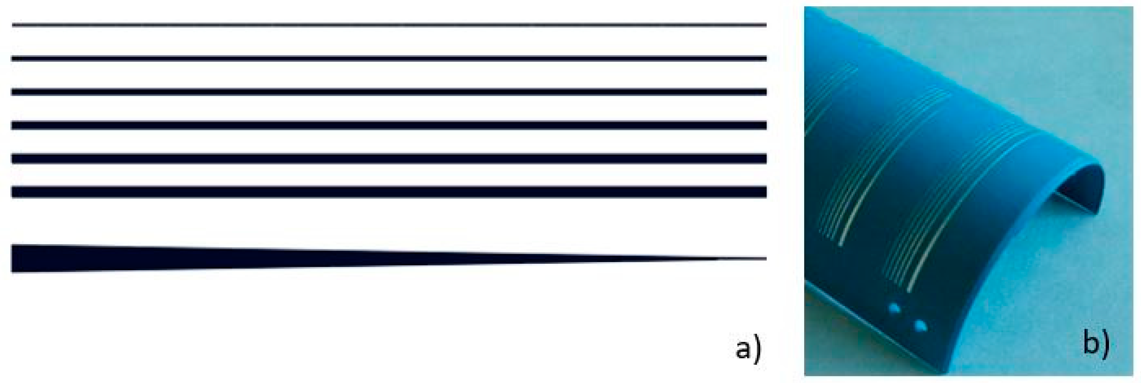
3.1. Shaping Results and Visual Inspection

The sintering experiments using free-form-assisted sintering revealed that standard sinter profiles can be applied without restriction. The substrates of technological levels 1 and 2 showed neither delamination nor other conspicuous defects. Only due to its self-weight, the LTCC multilayer adheres to the mold. If the dimension of the multilayer is larger than the half circumference of the mold, the overlapping material hangs down perpendiculary. Therefore, the curved length of the substrate is limited to the half circumference of the outer mold diameter and only half-cylinders can be achieved. The deviation of the obtained radius from the nominal value according Section 2.2 amounts to ±70 µm. As the mold can serve a simple quartz glass tube with a matching diameter, only one sheet of release tape is necessary as the auxiliary material. If the required design allows the half-cylinder geometry, this method is suitable for the production of curved multilayer substrates.
Cylinders encompassing almost 360° can be produced with form-assisted sintering. However, it is necessary to support the multilayer by an inner mold in order to prevent wrinkling. A pair of such molds is shown on Figure 7. A second release tape is necessary; therefore, the requirements for the molds are higher. The inner diameter of the outer mold and outer diameter of the inner one must match precisely the dimensions of the shaped circuit and thickness as well.
The sinter experiments at technological level 1 reveal that standard sinter profiles are not applicable. Figure 7b depicts a substrate obtained after standard sintering. The diffusion pathway for organic waste products is extremely long from the bottom region of the cylinder. Residues react with the inorganic ingredients and form the gray area visible at the bottom. The light blue area above still does not have the desired composition. Only the dark blue area on the top can be considered as a quality-assuring sintering product. The optimization of the sinter process results in a good homogeneity when the debinding phase is prolonged up to 180 min.
The accuracy of the formed radius when using this process amounts to r = 22.5 mm ± 0.050 mm. The shape fidelity is slightly higher in comparison with free-form sintering.
The tests at technological level 2 include 10 test substrates. It revealed that a conductor track width of at least 200 µm microns is required on the outer diameter to guarantee a reliable interconnect in 95% of the produced substrates. Since stretching of the surface occurs during deformation, it is necessary that enough conductor material is available for its compensation and thus to ensure a reliable electrical contact on the surface. Using narrower conductor tracks, electrical contact was given at only 60% of the test structures. The other 40% had cracks and no electrical contact from the beginning to the end of when the conductor track was measured. Therefore, a minimum width of 200 µm should be applied for a reliable electrical surface conductor path in further experiments. The results for gold and silver metallization are similar.
X-ray imaging reveals that conductor tracks of technological level 3 are more stable than those on the surface. We did not observe neither delamination, cracks nor warping for conductors with a line width of 175 µm or larger. Figure 8 depicts conductor paths with a line width of 100 µm. The via diameter amounts to 150 µm. Only one defect was observed in the array. The inspection of the via structures shows that vias with a 200 µm diameter lead to cracks along the bended substrate when their distance is smaller than 1 mm. Ten test substrates with a via diameter of 50 µm and 100 µm having a distance of 1000 µm between the vias were reliable at 97%. A decrease in reliability to 94% was noticeable when the diameter was increased to 150 µm. A further decrease in reliability was noticeable when the diameter was increased to 200 µm. Therefore, we recommend that the via diameter should not exceed 150 µm and be kept as small as possible with respect to the required functionality. The distance between two vias should be larger than 1 mm. Following these recommendations, the rejection rate should not exceed 5%.
If it is not possible to ensure the recommendations, this does not mean that a curved substrate cannot be manufactured. It just means the failure rate will increase.

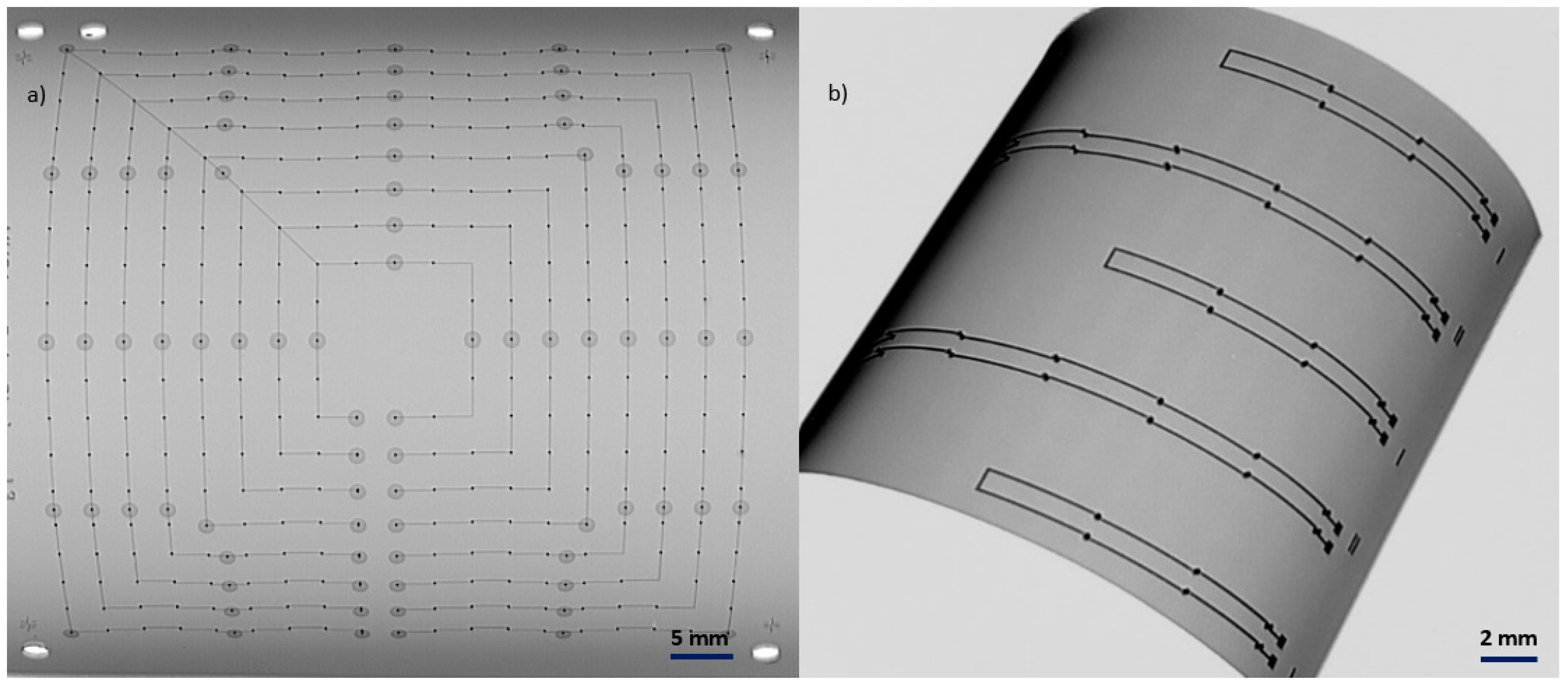
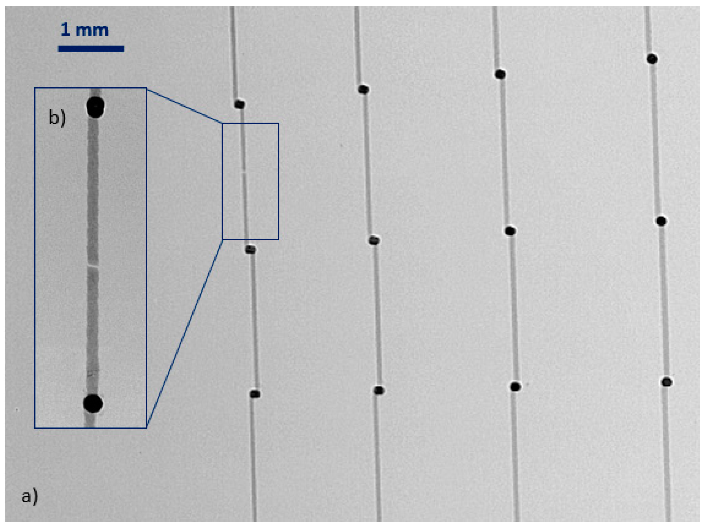
3.2. Electrical Properties of Internal Connections

Electrical measurements are carried out with a multimeter. The results for technological level 4 measured on daisy chains according to the layout in Figure 3 are summarized in Table 3.
The measured values vary strongly, and the lowest variation was obtained for substrate A. Substrate B showed the most short circuits and substrate C had no short circuit, but the resistance values had the highest deviation. A possible reason for the variation is the manual processing, which causes higher tolerances of printed structures. Enhanced by the deformation, the thickness and width of the conductor tracks are affected and lead to resistance changes.

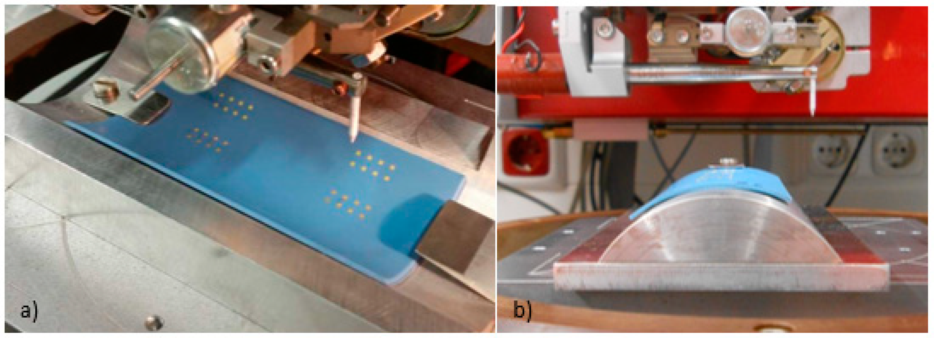
3.3. Assembly Aspects

The quality of the obtained bond connections depends on the surface curvature. The bond connections were conducted with the Bonder Delvotec 5410 (F&K Delvotec Bondtechnik GmbH, Ottobrunn, Germany). Figure 9a depicts a test piece with landing pads of gold. On the convex surface of the outer diameter, it was possible to generate reliable bonds only on the top. The limiting angle for the given geometry amounts to 35°, as illustrated in Figure 9b. Figure 9c–g reveal that pads within this position tolerance are well developed and well connected in both directions.
The geometric conditions for wire bonding on a concave surface are more inconvenient. Figure 10a shows a test substrate. The directional dependence of the bond connection is more strongly pronounced. Comparing Figure 10b–d makes it evident that bond connections in the direction of the circumference are very reliable (Figure 10b). Connections between landing pads in the center of the sample and bonding direction perpendicular to the circumference (Figure 10c) are also produced in good quality. However, when the position is shifted out of the middle, the wedge connection fails. As can be seen in Figure 10d, the two wires on the left have no adequate bond.
Soldering has been proven a more reliable connection technology. Figure 11a depicts the final demonstrator of the curved multilayer circuit, and Figure 11b shows the same thing mounted on a shaft. Since the demonstrator is a unique piece, all components were soldered manually. Due to this method, it was even possible to mount the wireless antenna chip with a large footprint without an additional cavity.

4. Conclusions and Outlook

We have proven in this work that LTCC multilayer circuits can be formed and mounted on curved surfaces. Two sinter methods are assessed to achieve the shape. A simple method is free-form sintering. Here, the multilayer is placed on a curved mold in the furnace. Additional effort is only necessary for the mold, and a quartz glass tube can be used for this purpose. Sinter profiles must not be changed. The shape fidelity amounts to 70 µm for the investigated geometry. A better shape fidelity of 50 µm can be achieved using form-assisted sintering. Moreover, it allows the production of almost closed cylinders. However, the method requires two geometrically matching molds and the sinter process must be adapted due to the limited outgassing cross-section. Due to the easier processing and shorter sintering times, free-form sintering is clearly preferable in terms of effort and costs. The shape tolerance fulfills the tolerance requirements of the targeted application.
Electrical connections should be designed with a width larger than 200 µm in order to prevent disruption of the wiring. The via diameter should be limited to 150 µm and the density should be kept as low as possible. As the minimum distance between two vias, we recommend 1 mm.
Wire bonding on the curved surface is possible with the restriction that the position of the bond should be on top of the curved multilayer. Components with a footprint of approximately 4 mm can be mounted without additional effort. For larger components, we recommend the use of cavities with graduated length in order to level the curvature.
We can thus conclude that it is possible to transfer the 2.5-dimensional LTCC technology into the third dimension. However, this work provides only a first feasibility analysis.
A lot of research still needs to be conducted and ideas have to be created in order to be able to manufacture and assemble even more complex geometric LTCC substrates with full functionality.

Author Contributions

Conceptualization, M.K.; Data curation, M.K.; Funding acquisition, J.M.; Investigation, M.K., T.H. and C.Z.; Methodology, M.K.; Writing—original draft, M.K.; Writing—review & editing, H.B. All authors have read and agreed to the published version of the manuscript.

Funding

This work was carried out within the project BisWind funded by Federal Ministry of Economic Affairs and Energy (funding code 0325891B) based on decisions of the German Bundestag.

Conflicts of Interest

The funders had no role in the design of the study, in the collection, analyses, or interpretation of data; in the writing of the manuscript, or in the decision to publish the results.

References

  1. Vitriol, W.A.; Johnson, G.W. Three Dimensional Microcircuit Structure and Process for Fabricating the Same from Ceramic Tape. U.S. Patent 5,028,473, 2 July 1991. [Google Scholar]
  2. Bauer, R.; Wolter, K.-J.; Sauer, W. Three Dimensionally Formed Thick Film Devices with LTCC Multilayer Technology. In Proceedings of the 1995 International Symposium on Microelectronics (ISHM), Los Angeles, CA, USA, 24–26 October 1995; pp. 481–487. [Google Scholar]
  3. Slosarcık, S.; Urbancık, J.; Pietriková, A.; Banský, J.; Bauer, R. LTCC based technology for 3D formed modules. J. Electr. Eng. 2004, 55, 265–268. [Google Scholar]
  4. Peterson, K.A.; Rohde, S.B.; Pfeifer, K.B.; Turner, T.S. Novel LTCC Fabrication Techniques Applied to a Rolled Micro Ion Mobility Spectrometer. In Proceedings-Electro-Chemi-Cal Society Pv; Electrochemical Society: Pennington, NJ, USA, 2004. [Google Scholar]
  5. Peterson, K.A.; Rohde, S.B.; Pfeifer, K.B.; Turner, T.S. Method for Producing a Tube. U.S. Patent 7,155,812, 2 January 2007. [Google Scholar]
  6. Peterson, K.A. Sandia Report. 2007. Available online: https://www.researchgate.net/publication/228780409_Macro-Meso-Microsystems_Integration_in_LTCC_LDRD_Report (accessed on 16 January 2021).
  7. Slosarčík, S.; Vehec, I.; Gmiterko, A.; Cabúk, P.; Jurčišin, M. Technology and Application of 3D Shaped LTCC Modules for Pressure Sensors and Microsystems. J. Microelectron. Electron. Packag. 2009, 6, 158–163. [Google Scholar] [CrossRef]
  8. Krueger, D.S.; Fadner, C.E.; Miller, G.V. Method and System for Fabricating Dome Shaped LTCC Substrates. U.S. Patent 8,968,637, 2 February 2015. [Google Scholar]
  9. Brandenburg, A.; Kita, J.; Groß, A.; Moos, R. Novel tube-type LTCC transducers with buried heaters and inner interdigitated electrodes as a platform for gas sensing at various high temperatures. Sens. Actuators B Chem. 2013, 189, 80–88. [Google Scholar] [CrossRef]
  10. Parrish, K.; Taff, J.; Yates, M.; Reis, D.; Plumlee, D. Plumlee, Characterization of the Fabrication Process of Rolled LTCC Structures. Int. J. Appl. Ceram. Technol. 2013, 10, 458–467. [Google Scholar] [CrossRef]
Figure 1. Scheme of form sintering: (a) preformed low-temperature cofired ceramics (LTCC) laminate; (b) free-form sintering: sintering the preformed low-temperature cofired ceramics (LTCC) laminate with the help of one mold and gravity; (c) form-assisted sintering: sintering the preformed LTCC laminate between two molds for dimensional accuracy.
Electronics 10 00248 g001
Figure 2. Test structures for surface metallization: (a) test layout, width variation for lines from 70 µm to 200 µm; (b) printed layout on the sintered multilayer.
Electronics 10 00248 g002
Figure 3. X-ray images of the two different daisy chains; (a) daisy chain sized 60 mm × 60 mm; (b) daisy chain sized 30 mm × 4 mm.
Electronics 10 00248 g003
Figure 4. Calculated deviation from the comparison of the measured substrate to the theoretical design (µm).
Electronics 10 00248 g004
Figure 5. Adaption of the bonder Delvotec 5410 to shaped LTCC substrates: (a) concave shape for bonds on the inner diameter and (b) convex shape for bonds on the outer diameter.
Electronics 10 00248 g005
Figure 6. Laser scanning microscope image of a cavity: (a) view along the cavity, demonstrating the height difference of the curved surface and cavity; (b) three-dimensional view illustrating the flatness of the cavity.
Electronics 10 00248 g006
Figure 7. Form-assisted-sintering: (a) mold with matching inlay; (b) sintering results after use of a standard profile; (c) successful sintering achieved by extending the debinding time.
Electronics 10 00248 g007
Figure 8. X-ray image of conductor tracks: (a) array of intact conductor tracks with a width of 100 µm; (b) detail of an interruption.
Electronics 10 00248 g008
Figure 9. Convex test substrate for wire bonding: (a) position of the landing pads; (b) limiting angle for successful bonding; (cg) details of the obtained bond connections.
Electronics 10 00248 g009
Figure 10. Bond connections on a concave substrate. (a) position of landing pads; (bd) details of the obtained bond connections.
Electronics 10 00248 g010
Figure 11. Shaped substrate fully equipped and ready to use manufactured by Mirco Systems Engineering GmbH. (a) fully equipped substrate; (b) equipped substrate placed on the steel shaft as in the intended use.
Electronics 10 00248 g011
Table 1. Overview of the different technological stages and used materials.
Name of Sample GroupDegree of ComplexityMaterial
level 1only LTCC substrateDP 951 PX
level 2surface metallizationDP 6145, DP 6146,
DP 5740A, DP 5742
level 3inner conductor lines and viasDP 6145, DP 6141, DP 6138
level 4daisy chainsDP 6145, DP 6141, DP 6138
level 5complex layout with assembled componentsDP 5740A, DP 5742, DP 6138, DP 6141, DP6145, DP 6146
Table 2. Parameters for bonding.
BallWedge
Utrasonic time (ms)200200
Ultrasonic power (digits)120120
Bondforce (cN)2520
Table 3. Resistance measurements of daisy chains (30 mm × 4 mm).
SubstrateChain No.
12345
Resistance (Ω)Resistance (Ω)Resistance (Ω)Resistance (Ω)Resistance (Ω)
A0.270.410.420.4Open circuit
BOpen circuitOpen circuit1.260.70.4
C1.290.671.320.670.35
Publisher’s Note: MDPI stays neutral with regard to jurisdictional claims in published maps and institutional affiliations.

