Article

Net-Shape-Based Automated Detection of Integrated-Circuit Layout Plagiarism

Institute of Microelectronics and Optoelectronics, Warsaw University of Technology, 00-661 Warsaw, Poland
*
Author to whom correspondence should be addressed.
Electronics 2021, 10(24), 3181; https://doi.org/10.3390/electronics10243181
Submission received: 14 November 2021 / Revised: 14 December 2021 / Accepted: 16 December 2021 / Published: 20 December 2021
(This article belongs to the Section Microelectronics)

Abstract

:
Plagiarism of integrated-circuit (IC) layout is a problem encountered both in academia and in industry. A procedure was proposed that compares IC layouts based on the physical representation of particular electrical nets, i.e., on the shape of the features drawn on conducting layers (metals and polysilicon). At the heart of this method is the Needleman–Wunsch algorithm, used for decades in tools aligning sequences of amino acids or nucleotides. Here, it is used to quantify the visual similarity of nets within the pair of layouts being compared. The method was implemented in Python and successfully used to identify clusters of similar layouts within two pools of designs: one composed of logic gates and one containing operational transconductance amplifiers.

1. Introduction

Software tools are used to detect plagiarism in many fields. The most mature and widespread is software analyzing natural language in the search of plagiarism in student essays, theses, and other bodies of text [1]. In addition, gaining in popularity are tools for comparing source code files—see [2] for an overview and [3,4] for an example of latest advances. On the other hand, much less work seems to have been dedicated to creating equivalent systems for comparing integrated circuit (IC) layouts. One of the few exceptions is described in the series of publications [5,6,7,8]. A methodology for IC layout comparison is proposed in [5], while software based on this methodology is described in [6,7,8]. The procedures presented there are mostly based on comparing statistical parameters of layouts such as the number of metal layers used, cumulative area of shapes on each layer, or number of devices and other shapes. As such, this methodology is mostly relevant to large VLSI systems. The comparison on the level of individual cells is limited to XOR-ing the cells’ layouts to detect similarly shaped and placed components. This approach surely works for cases of downright plagiarism of VLSI circuits, where the copied design is synthesized either using standard cells from the same provider as the original or using (nearly) exact copies of those standard cells. However, cases where the layout of one circuit is just “heavily inspired” by another may go undetected.
The method proposed earlier by the authors of this paper in [9,10] was dedicated specifically to the quantification of similarity between the layouts of relatively simple building blocks. That effort was motivated by cases of plagiarism encountered by one of the authors during his teaching career. Students participating in a microelectronics course lack both experience and time, which vastly restricts the complexity of circuits that can be used as assignments. Thus, simple blocks such as logic gates, flip-flops, or amplifiers are used over and over as assignments. This repeatability makes copying a very tempting choice for students. Indeed, cases of plagiarism were frequently observed by the authors. Of course, the visual similarity of the two layouts is not a proof of cheating, and each case must be analyzed individually. Still, a tool screening a large pool of designs in search or pairs (or larger clusters) of similar-looking solutions would be welcome.
The two most obvious criteria that can be used to compare two layouts are location of devices (transistors, diodes, and passives) and the shape of interconnects (“wires”) linking those devices. The transistor-based approach has been exhaustively described in [9,10]. One might argue, however, that the network of interconnects is a better “fingerprint” of a circuit layout than the transistor placement. Even if the location of individual transistors was fixed, various designers may still choose different ways to route wires between them. The opposite is not true, since the shape of the interconnect network largely determines the location of transistors. Moreover, if the definition of “interconnect” is extended to include transistor gates, the shapes of interconnects provide almost the complete information about the layout appearance.

2. Methods

The method presented in this paper compares IC layouts based on the shapes of their nets. A net is defined here as the set of electrically connected shapes on conducting layers, i.e., polysilicon and metal layers. All the polygons drawn on those layers are extracted from the original layout. Subsequently, nets are formed by identifying subsets of polygons connected by vias or contacts. Finally, all the polygons within each net are merged (flattened) to remove superfluous vertices. The layout of a logic gate along with its nets extracted this way are shown in Figure 1.
The merging stage transforms a layout from a large set of relatively simple shapes into a smaller set of polygons that are more complex and thus more distinct. Inclusion of polysilicon features, being mostly MOSFET gates, makes this method sensitive not only to the shapes of interconnects but also to the size and orientation of MOSFETs.
The proposed method of plagiarism detection has two main components: identification of corresponding nets in a given pair of layouts and quantification of the visual similarity between corresponding nets. These two stages are described below.

2.1. Identification of Corresponding Nets

As shown in the next subsection, the cost of comparing two nets (i.e., quantifying their visual similarity) is approximately quadratic in their size. This relatively high computational complexity makes it impractical to compare all the possible net pairs in two layouts in the search for the best match. Thus, some other way must be found to identify the corresponding nets in the layouts being compared. If the circuit diagrams of these designs were guaranteed to be identical, one could try analyzing their topologies to find corresponding nets. However, this assumption is not always met. Therefore, a more flexible approach is proposed that pairs nets based on the shape of their convex hulls.
First, the centroid of every net is shifted to ( 0 , 0 ) , and the net’s convex hull H is built (see Figure 2a). Then, for every possible pair of nets in the two designs, the intersection and union of their convex hulls are found (Figure 2b). Subsequently, for every pair of nets, say m and n, the following expression is calculated:
S ( H m H n ) S ( H m H n ) ,
where S ( · ) denotes the surface area of a given polygon. The net that maximizes this ratio for a given net in the other layout is considered its counterpart. Please note that overlapping convex hulls of nets instead of the nets themselves makes the method more robust against slight differences in net shapes. The union of the hulls is used in the denominator to prevent the largest nets from being wrongly matched to some other nets just due to their size. This method is not guaranteed to couple every net in one layout with exactly one net in the other. This may be seen as an advantage, because if the number of nets differs between the layouts being compared, no net is left without a counterpart.

2.2. Comparison of Corresponding Net Shapes

The initial approach adopted in this work relied on comparing nets based on their fundamental geometric properties. Those included the centroid, surface area, perimeter, moment of inertia, and moment invariants. However, it soon turned out that a single parameter, or even a linear combination of all the parameters listed above, is insufficient to capture enough properties of a polygon to reliably express visual similarity between two nets.
A better approach relies on representing the border (perimeter) of a polygon as a sequence of fixed-length vectors. Since most shapes on IC layouts are aligned along one of the two principal axes, those vectors point in one of four directions. Thus, each of them can be encoded as one of the four cardinal directions, i.e., N, S, W, or E. This way, the entire border of a polygon can be encoded as a string composed of those four symbols. The application of this idea to the nets from Figure 2 is shown in Figure 3. The black dots mark the initial point of the sequences.
Once two nets are encoded as strings, the dissimilarity between them may be expressed in a quantitative manner. In the simplest case, it is defined as the edit distance or the minimum number of basic operations necessary to align those strings, i.e., transform one into the other. Two such transformations are possible:
  • In the case of a mismatch between corresponding symbols in the two strings, a symbol copied from one of them replaces its counterpart in the other.
  • A symbol copied from one string is inserted into a gap made between symbols in the other string. This is equivalent to deleting the symbol from the original string. Either way, the length of one of the strings is modified.
Figure 4 shows one possible alignment of the strings describing nets A and B from Figure 3.
Aligning these strings requires inserting two “missing” symbols into the top string and two other into the bottom string. The gaps made for the inserted symbols are denoted as dashes and marked in blue. In spite of the four insertions, though, a mismatch between letters S and N (marked in yellow) was unavoidable in the presented example. Other solutions, i.e., different locations of insertions and mismatches, are possible for this example. It can be easily shown, however, that the total number of those basic operations cannot be less than five, which is the actual edit distance between those two strings.
If a negative (or zero) weight is assigned to each matching pair of letters while insertions and mismatches carry positive weights, the best alignment between two strings can be defined as one that minimizes the sum of those weights. Finding such an alignment becomes an optimization problem known as edit distance minimization (see, e.g., [11], Chapter 6.3). This is the task performed, e.g., by spell checkers searching a dictionary for the best match for a misspelled word. In the simplest formulation of this problem, a mismatch and an insertion incur the same penalty. However, differentiating the cost of these two transformations may be useful in the context of comparing polygons with respect to their shape. An insertion is usually performed to match two identically oriented edges of different lengths. The last two insertions in Figure 4, for instance, are necessary because nets A and B differ in the length of the branches pointing left and down. Still, such a size difference between two nets does not make them much different visually. A mismatch, on the other hand, corresponds to a pair of similarly sized but differently oriented edges—see the mismatch in Figure 4, corresponding to differently oriented “jogs” in the horizontal parts of nets A and B. Differences in direction are easier to spot visually than differences in length. More importantly, the presence of differently oriented edges may suggest that the two interconnects are routed into different parts of their respective cells, thus making the entire cells look different. For these reasons, it seems reasonable to penalize mismatches more heavily than insertions.
The best alignment between two sequences of symbols is usually found using dynamic programming. In the case where the costs of insertions and mismatches are allowed to differ from each other, the procedure of choice is the Needleman–Wunsch algorithm (NWA) [12]. This method was used for decades to align sequences of amino acids or nucleotides. However, it has also found numerous applications outside biology and chemistry.
One of several possible formulations of the NWA uses a positive cost d of an insertion as well as a function s ( i , j ) , whose value depends on whether the i-th symbol in the first string and the j-th symbol in the second string match or not. Comparing an m-letter string with another, n-letter string, starts with building an m-by-n matrix F. Its entry (i, j) corresponds to the cost of optimal alignment of the first i characters of the first string with the first j characters of the second string. The strings are analyzed from left to right; therefore, the matrix is filled out starting from the top-left corner (alignment of two empty strings) until the bottom-right entry is inserted (cost of aligning the complete strings). The matrix is initially empty with the exception of the first column and first row. The i-th entry in the first column corresponds to the cost of aligning the first i characters in the first string to an empty string. This task requires copying all the first i letters from the first string into an empty sequence, with each such insertion entailing the cost d. Thus, subsequent entries in the first column are d, 2 d , …, m d . Similarly, the j-th entry in the first row corresponds to the cost of aligning the second string to an empty sequence, so this row is filled out in the same way. The rest of matrix F is then filled out from left to right and from top to bottom, which corresponds to aligning increasingly long subsequences of both strings starting from the beginning. Every step must minimize the aggregate cost of such an alignment, i.e., the cost including all the previous steps. Matching the i-th symbol in the first string with the j-th symbol in the second one may be performed in one of three ways:
  • The i-th symbol is copied from the first string into the second one;
  • The j-th symbol is copied from the second string into the first one;
  • No modifications are made, and the cost of this step depends on whether or not the symbols match.
Out of those three possibilities, the operation minimizing the aggregate cost is chosen. Using the matrix notation, this choice can be written as:
F [ i , j ] = min F [ i 1 , j ] + d , F [ i , j 1 ] + d , F [ i 1 , j 1 ] + s ( i , j ) .
After filling out a row (or column), the procedure is performed for the next row (or column) until the entire matrix is filled. The bottom-right entry is the last to be evaluated. It contains the full cost of matching the entire strings.
The following example illustrates the determination of optimal alignment cost of strings a = NESW and b = NEENW . The costs of single-symbol mismatch and match are assumed here to be:
s ( i , j ) = 2 , a [ i ] b [ j ] ( mismatch ) , 0 , a [ i ] = b [ j ] ( match ) ,
while the insertion cost is d = 1 . These values reflect the idea that, as previously stated, a mismatch should be penalized more heavily than an insertion, while a match should entail no cost. Figure 5 shows the matrix used to achieve the optimal alignment.
Arrows leaving a cell point to all the optimal alignments of strings that can be transformed into the given string by making one of the basic operations. An upward-pointing arrow leaving cell ( i , j ) means that the optimal choice is to copy the i-th symbol from NESW into NEENW—case ➀ in Formula (2). An insertion from NEENW into NESW (case ➁) is indicated by a left-pointing arrow. A diagonal arrow means that matching the i-th character of NESW with the j-th character of NEENW is the best choice (case ➂). Pursuing the path from the bottom-right cell to the top-left one while performing the appropriate operation at each step allows one to reconstruct the optimally aligned strings. In some cases, two or three choices result in the same cost, which is reflected by two or three arrows leaving the cell. The example at hand has several optimal solutions, two of which have been plotted as colored paths. The solid orange line corresponds to string b being transformed into NE–SW, while the dashed blue line corresponds to this string being transformed into NES–W. All the optimal alignments have a cost of 3, which is the bottom-right entry in the matrix. The actual transformations are of no interest in the context of IC layout comparison. What is important to note, however, is that if both strings are encoded as sequences of a similar length, say l characters, the entire procedure of filling the matrix takes O ( l 2 ) time.
The proportion between the number of errors, i.e. insertions and mismatches, and the string length after the alignment (aligned strings have by definition identical lengths) is used as a measure of distance between the nets represented by those strings. In the case of strings in Figure 4, the distance is thus 5 / 28 . On the level of entire layouts, the distance Δ between a pair of designs is defined as the average distance between all the pairs of corresponding nets.

2.3. Algorithm Tuning

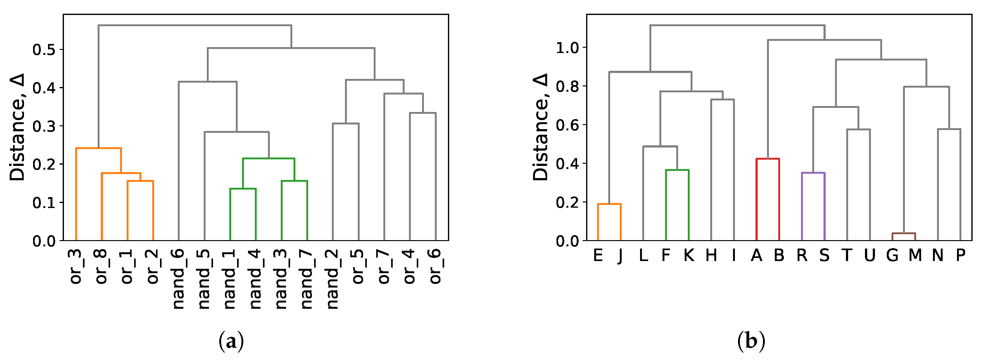
The procedure outlined above has several parameters, whose values affect both its execution time and accuracy. Some suggestions are provided below as to the choice of those values. This choice was validated using three benchmarks composed of operational transconductance amplifiers (OTAs), NAND gates, and OR gates. Within each benchmark, some layouts were considered “visually similar”. Table 1 sums up the composition of each benchmark.
The layouts of those circuits were designed for a legacy technology used at the authors’ university to teach microelectronic design basics. The minimum MOSFET gate length in this technology is 1 μ m . The logic cells had a height between 30 and 54 μ m , while the OTA layouts measured between 150 and 200 μ m on a side.
One of the essential parameters to consider while encoding the nets as strings is the symbol length  λ , defined here as the length of a net edge to be encoded as a single symbol (“character”) in a string. Intuitively, a smaller λ should provide better resolution, and hence superior accuracy, at the expense of a longer running time. The minimum value worth considering is the feature size of the target technology. Such a choice, however, would lead to nets being encoded as very long strings, which in turn would negatively impact the execution time. Therefore, the symbol length was tentatively chosen as 5 μ m , i.e., five times the process feature size and approximately one-tenth the logic gate height. This choice is justified later in this section.
Another important decision had to be taken regarding the encoding of edges shorter than λ as well as the “remainders” of those edges whose lengths are not a multiple of λ . Such edges and edge parts may be either encoded as symbols or ignored, as shown in Figure 6a,b, respectively.
Solution (a) was used in this work, since it has been shown to consistently lead to smaller errors at the expense of producing slightly longer strings. However, it was decided to ignore any edges shorter than 0.75 μ m . This serves to smooth out small “jogs” in net borders.
As explained before, the insertion cost d used in the NWA is allowed to differ from the mismatch cost. What matters is actually the ratio between those two quantities; therefore, the mismatch cost was assumed to be unity. As for the insertion cost 
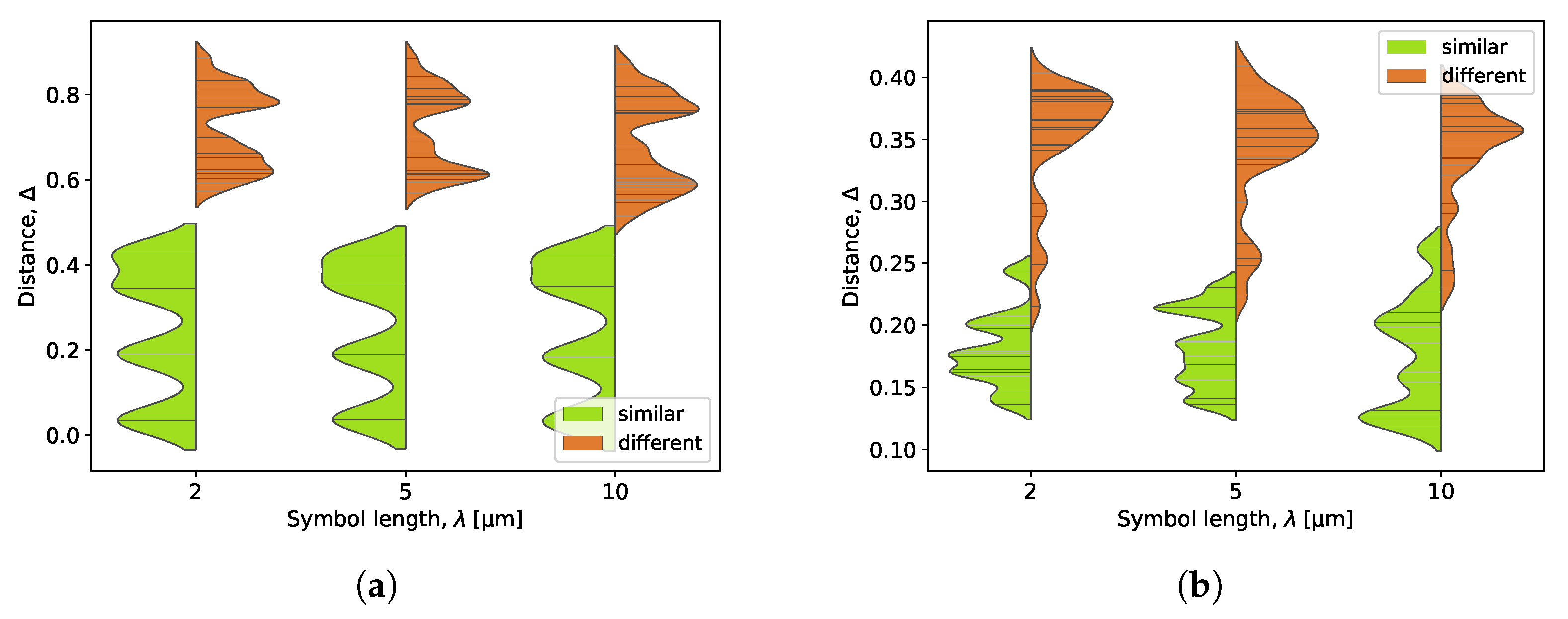
d, several values were tested while running the proposed procedure on the benchmarks. The NAND and OR gates were pooled together in this experiment in order to increase the sample size. OTAs were analyzed separately because of their significantly larger dimensions. Within each of those groups, all possible pairwise comparisons were performed. Statistical distributions of distance Δ obtained for several values of d were approximated using kernel density estimations. The distributions were plotted in Figure 7 separately for visually similar pairs (green) and for different ones (red). Since some differences in net shapes and sizes occur even in “similar” designs, increasing the insertion cost inevitably translates into greater values of Δ both for different pairs and for similar ones. What matters, however, is not the value of Δ but the separation between the two distributions. Ideally, the “most similar among the different” pairs should have a Δ greater than the “most different among the similar” ones. As regards OTAs, this is indeed the case irrespective of d. As for logic gates (Figure 7b), the separation is never perfect, but it improves as d drops below unity. Interestingly, reducing the insertion cost d further, below about 0.5 , does not change the distributions any more. This may be because insertions become so inexpensive that any shape difference between nets can be canceled by inserting an appropriate number of symbols into one or both nets, without the need to accept a relatively expensive mismatch. Based on the results of this experiment, the value d = 0.5 was chosen for the rest of this work.
The same experimental setup was used to validate the choice of symbol length. As shown in Figure 8, the value λ = 5 μ m used so far provides a better separation of “similar” and “dissimilar” cases than λ = 10 μ m . Further reduction of λ to 2 μ m does not visibly affect the distributions while producing longer symbol strings, which adversely affects the computation time.
To conclude, the most reasonable settings for the proposed procedure seem to be: symbol length λ about five times the minimum feature size and insertion cost d = 0.5 .

3. Results

The proposed method was implemented in Python. The third-party Polygon3 package was used for operations such as polygon merging or determination of convex hulls [13]. After the identification of key parameter values as explained in Section 2.3, the program was tested on student projects designed for the same 1 μ m technology as the benchmark circuits. A proprietary tool Excess [14], developed at the authors’ university, was used to extract nets from the layouts.
The rest of this section is divided into two parts. Section 3.1 discusses the quality of clustering, i.e., grouping layouts based on their similarity, achieved with the proposed method. To facilitate the visual assessment of the obtained results, this analysis was performed on relatively small samples of circuits of two types: 15 logic gates and 17 operational transconductance amplifiers. The samples were built so as to contain circuit pairs with a varying degree of similarity, ranging from nearly identical to definitely different.
Section 3.2, on the other hand, shows how the performance of the proposed algorithm is impacted by factors such as the average number of nets in a layout or the number of symbols used to encode a single net. Analytical estimates are confirmed by an experiment performed on a sample of 59 OTAs.

3.1. Accuracy

First, a set of 15 logic gates was analyzed, including 7 NAND- and 8 OR-gates. The results of this pairwise comparison are presented in Figure 9a in the form of a dendrogram [15]. The layouts of all the gates are presented in Figure A1 in Appendix A. To make visual inspection easier, these layouts are arranged in the same order as in the dendrogram.
In a dendrogram, the height of a link between two nodes (gate layouts in this case) or node clusters corresponds to the distance Δ between them. In the case of single layouts, the distance between them is evaluated using the approach presented in Section 2. The distance between entire clusters, however, may be defined in many alternative ways [15]. It may be as simple as the distance between the “most distant” or, conversely, the “nearest” members of the two clusters. The former measure proved too restrictive for our needs, while the latter tended to build oversized clusters. Hence, more complex approaches were tried, exploiting the concept of weighted averaging or variance analysis. Among those methods, the one minimizing the Ward variance yielded clusters that best reflected the visual similarity between some layouts and difference between others [16]. This method was chosen for use throughout the rest of the study.
In the first experiment the NAND and OR gates were deliberately analyzed together to see if the proposed method can separate gates implementing those two logic functions just based on the shapes of their nets. As shown in Figure 9a, such separation proved almost perfect, with 6 out of the 7 NAND gates forming a separate cluster. Within the all-NAND group, a cluster of four gates was identified (marked in green), whose distance from one another is particularly small. As can be seen in Figure A1, each of those four gates (also drawn in green) has a layout containing four C-shaped nets and one I-shaped net. Other NAND gates were drawn differently, which also sets them apart in the dendrogram. A group of four mutually similar layouts also exists among the OR gates (marked in orange). Visual inspection of layouts in Figure A1 (also drawn in orange) makes evident both their mutual similarity and their difference from other OR-gate designs.
A similar experiment was carried out with operational transconductance amplifiers (OTAs). Those circuits exceed logic gates in terms of the size and complexity of their nets. The dendrogram for a pool of 17 OTAs is shown in Figure 9b. The layouts themselves are presented in Figure A2 in Appendix A, with the order and coloring the same as in the dendrogram. Let us analyze layout pairs starting from those corresponding to the bottom-most dendrogram links. The device placement in layouts G and M is identical, with some interconnects routed differently in an attempt to conceal the cheating. However, since MOSFET parts, i.e., polysilicon gates and metal regions covering the drain and source areas, constitute significant portions of nets analyzed in this work, the different interconnect routing was not sufficient to blur the similarity of those two layouts. The same goes for pair E-J and, to a lesser degree, F-K. The similarity of designs A and B results from the almost identical, intricate networks of interconnects linking transistors in the left-hand side of the design. This similarity was detected in spite of other parts of the designs being noticeably different. In addition, the interconnect patterns in designs R and S were correctly classified as similar in spite of substantially different aspect ratios of those two layouts. Other design pairs are visibly distinct.

3.2. Performance

An estimate of the computational complexity of the proposed method is presented below. Since comparison makes sense only for similarly complex layouts, we assume the same number of nets n in each circuit. The number of vertices describing a given net is denoted as p. After the net is transformed into a string of symbols, its length is denoted as l. Since every edge in a polygon translates into at least one symbol, it is assumed that l p for a given net.
The initial step, i.e., finding the convex hull for each net in each layout, takes O ( p log p ) time per net [17]. Then, for each net in one layout, its convex hull is successively overlapped with the hulls of all the nets in the other layout. Each such operation is followed by the calculation of the intersection and union of the overlapped hulls. These operations take O ( p log p ) time per pair, where p is the total number of vertices in the pair of convex hulls. One can assume that the convex hull of a net contains fewer vertices than the net itself, such that p < p . Then, the surface area of the resulting intersection and union are calculated, which takes O ( p ) . This takes place for each pair of nets in the two layouts, such that the total complexity of identifying all the corresponding nets in a layout pair is bounded by O ( n 2 p log p ) . Finally, the NWA is performed for each of the n pairs of corresponding nets with a total time complexity of O ( n l 2 ) .
For circuits the size of an operational amplifier, with about a dozen nets, most of them encoded as strings of 60 to 300 symbols, the computation time seems dominated by the NWA. To validate this claim, a pairwise comparison of 59 OTA layouts was run on a Linux machine with an AMD Ryzen 5 4600H and 16 GB RAM. Figure 10 shows the relationship between the layout comparison time and the string length. The running time was in each case divided by the average number of nets in the pair of layouts being compared. In addition, the string lengths were averaged over all the nets in both layouts. To confirm the O ( n l 2 ) estimate of computation time, a power-law curve was fitted to the data. The fit resulted in an exponent of 1.997 , which agrees well with the assumption of a quadratic relationship between the average string length and computation time per net. Attempts to replace the average string length with the maximum or median length led to relationships with much smaller coefficients of determination. Thus, the net count and the average number of symbols used to encode a net in a given layout are sufficient to predict the analysis time with good accuracy.
The convex hulls of the n nets in a layout can be found independently from one another, just like the (approximately) n 2 hull intersections and unions. Likewise, the NWA-based computations of n distances between pairs of corresponding nets can be performed concurrently. Therefore, the procedure of comparing two layouts can easily be parallelized.

4. Discussion

The procedure proposed in this paper, implemented in Python, proved successful in detecting all the pairs and larger clusters of similar designs in two pools of layouts: logic gates and OTAs. It is convenient to plot the analysis results as a dendrogram. The height of the link between dendrogram nodes reflects accurately the visual dissimilarity of the corresponding layouts. The user of the tool can subsequently inspect the designs visually, working his or her way through pairs with increasing values of Δ (e.g., pairs G-M, E-J etc. in Figure 9b) until no similarity is noticed. Such inspection, limited to several layout pairs, is relatively efficient. In the absence of the tool, a visual search for similar shapes within a pool of dozens of layouts would be an overwhelming task.
The choice of symbol length λ is crucial to obtaining accurate results in a reasonable time. The average number of symbols used for encoding a net has a relatively strong (quadratic) impact on the total analysis time. The results obtained in this work suggest that splitting the average net into about 100 to 200 symbols provides good accuracy even for relatively large cells such as OTAs. For smaller cells with simpler nets, such as logic gates, as few as 20 to 30 symbols per net proved sufficient. These numbers correspond to the symbol length λ five times the minimum feature size used in the layouts.
Cell dimensions are not normalized in any way prior to the comparison. The reason is that the size and aspect ratio are regarded as traits that make a cell unique. One might argue that without size normalization the proposed approach is vulnerable to cases where a substantially resized copy of the original cell is created just to make the two look different. This scenario, however, is unlikely since the designer, whether a professional or a student, is almost always forced to make the layout as compact as possible. This reasoning is true as long as all the layouts being compared are designed for the same technology or at least for technologies with the same minimum feature size. If this is not the case, some scaling between the process nodes must be applied. Also, for every pair of cells, it might be worth performing two comparisons, with the second one preceded by flipping one of the cells horizontally. Vertical flipping seems to make less sense, especially in the case of logic cells as long as some assumption is made as to the location of the ground and power rails.
The analysis of layouts in Figure A1 (see Appendix A) clearly demonstrates that, in spite of the overall visual similarity of some layouts, the exact sizes, shapes, and locations of their corresponding nets are far from identical. Hence, it is unlikely that simply XOR-ing layout images would be enough to distinguish between similar and different layouts.

Author Contributions

Conceptualization, D.K.; methodology, D.K. and M.H.; software, M.H. and D.K.; validation, M.H.; formal analysis, M.H. and D.K.; investigation, M.H.; resources, not applicable; data curation, M.H. and D.K.; writing—original draft preparation, D.K.; writing—review and editing, D.K.; visualization, D.K. and M.H.; supervision, D.K.; project administration, D.K.; funding acquisition, not applicable. All authors have read and agreed to the published version of the manuscript.

Funding

This research received no external funding.

Conflicts of Interest

The authors declare no conflict of interest.

Abbreviations

The following abbreviations are used in this manuscript:
ICintegrated circuit
NWANeedleman–Wunsch algorithm
OTAoperational transconductance amplifier
VLSIvery large-scale integration

Appendix A. Layouts

Presented at the end of this paper are designs, i.e., nets extracted from the layouts, used in Section 3 for validating the proposed method. The ordering and coloring of the designs are the same as in the corresponding dendrograms.
Figure A1. Nets extracted from the pool of NAND and OR gates whose mutual similarity was shown in the dendrogram in Figure 9a.
Electronics 10 03181 g0a1
Figure A2. Nets extracted from the 17 OTAs whose mutual similarity was shown in the dendrogram in Figure 9b.
Electronics 10 03181 g0a2

References

  1. Chowdhury, H.A.; Bhattacharyya, D. Plagiarism: Taxonomy, Tools and Detection Techniques. arXiv 2018, arXiv:1801.06323. [Google Scholar]
  2. Novak, M. Review of source-code plagiarism detection in academia. In Proceedings of the 2016 39th International Convention on Information and Communication Technology, Electronics and Microelectronics (MIPRO), Opatija, Croatia, 30 May–3 June 2016; pp. 796–801. [Google Scholar] [CrossRef]
  3. Wu, J.S.; Chien, T.H.; Chien, L.R.; Yang, C.Y. Using Artificial Intelligence to Predict Class Loyalty and Plagiarism in Students in an Online Blended Programming Course during the COVID-19 Pandemic. Electronics 2021, 10, 2203. [Google Scholar] [CrossRef]
  4. Kurtukova, A.; Romanov, A.; Shelupanov, A. Source Code Authorship Identification Using Deep Neural Networks. Symmetry 2020, 12, 2044. [Google Scholar] [CrossRef]
  5. Chari, K.S.; Sharma, M. Integrated circuit layout design screening. In Proceedings of the 2013 IEEE Conference on Information Communication Technologies, Thuckalay, India, 11–12 April 2013; pp. 1305–1308. [Google Scholar] [CrossRef]
  6. Chari, K.; Sharma, M. Assessment and comparison of IC Layout Designs. In Proceedings of the 2011 International Conference on Signal Processing, Communication, Computing and Networking Technologies, Thuckalay, India, 21–22 July 2011; pp. 798–805. [Google Scholar] [CrossRef]
  7. Chari, K.S.; Sharma, M. Custom tools for IC LD evaluation. In Proceedings of the 2013 IEEE Conference on Information Communication Technologies, Thuckalay, India, 11–12 April 2013; pp. 1299–1304. [Google Scholar] [CrossRef]
  8. Chari, K.S.; Sharma, M. Performance of IC layout design diagnostic tool. In Proceedings of the 2015 Global Conference on Communication Technologies (GCCT), Thuckalay, India, 23–24 April 2015; pp. 332–337. [Google Scholar] [CrossRef]
  9. Kasprowicz, D.; Wada, H. Computer-aided detection of plagiarism in integrated-circuit layouts. In Proceedings of the 20th International Conference Mixed Design of Integrated Circuits and Systems—MIXDES 2013, Gdynia, Poland, 20–22 June 2013; pp. 213–217. [Google Scholar]
  10. Kasprowicz, D.; Wada, H. Methods for automated detection of plagiarism in integrated-circuit layouts. Microelectron. J. 2014, 45, 1212–1219. [Google Scholar] [CrossRef]
  11. Dasgupta, S.; Papadimitriou, C.H.; Vazirani, U. Algorithms, 1st ed.; McGraw-Hill, Inc.: New York, NY, USA, 2006. [Google Scholar]
  12. Needleman, S.B.; Wunsch, C.D. A general method applicable to the search for similarities in the amino acid sequence of two proteins. J. Mol. Biol. 1970, 48, 443–453. [Google Scholar] [CrossRef]
  13. Rädler, J. The Polygon3 Package for Python. Available online: https://pypi.org/project/Polygon3/ (accessed on 7 May 2021).
  14. Niewczas, M.; Wojtasik, A. Modeling of VLSI RC parasitics based on the network reduction algorithm. IEEE Trans. Comput. Aided Des. Integr. Circuits Syst. 1995, 14, 137–144. [Google Scholar] [CrossRef] [Green Version]
  15. Hastie, T.; Tibshirani, R.; Friedman, J. The Elements of Statistical Learning: Data Mining, Inference and Prediction, 2nd ed.; Springer: New York, NY, USA, 2009. [Google Scholar]
  16. Ward, J.H. Hierarchical Grouping to Optimize an Objective Function. J. Am. Stat. Assoc. 1963, 58, 236–244. [Google Scholar] [CrossRef]
  17. de Berg, M.; van Kreveld, M.; Overmars, M.; Schwarzkopf, O. Computational Geometry: Algorithms and Applications, 2nd ed.; Springer: Berlin/Heidelberg, Germany, 2000; p. 367. [Google Scholar]
Figure 1. One of the logic gates analyzed in this work: (a) its full layout and (b) its nets after merging.
Electronics 10 03181 g001
Figure 2. (a) Two nets A and B and their convex hulls H A and H B . The cross denotes the net’s centroid after shifting to ( 0 , 0 ) . (b) Union H A H B and intersection H A H B of those hulls.
Electronics 10 03181 g002
Figure 3. The nets from Figure 2 with their borders encoded as sequences of symbols starting from the top-left corner (black dot).
Electronics 10 03181 g003
Figure 4. One of the optimal alignments of strings representing the polygons from Figure 3. A mismatch is marked in yellow, while insertions are marked in blue.
Electronics 10 03181 g004
Figure 5. A matrix built with the Needleman–Wunsch algorithm for strings NESW and NEENW.
Electronics 10 03181 g005
Figure 6. Two possible approaches to encoding polygon edges whose lengths are not a multiple of the symbol length λ : (a) edges (and edge fragments) shorter than λ are encoded as symbols; (b) such edges are ignored.
Electronics 10 03181 g006
Figure 7. Distribution of distance Δ calculated for two benchmarks using various values of insertion cost d: (a) benchmark composed of OTAs; (b) benchmark composed of NAND and OR gates.
Electronics 10 03181 g007
Figure 8. Distribution of distance Δ calculated for two benchmarks using various values of symbol length λ : (a) benchmark composed of OTAs; (b) benchmark composed of NAND and OR gates.
Electronics 10 03181 g008
Figure 9. Application of the proposed method to the benchmarks: (a) benchmark composed of NAND and OR gates analyzed together; (b) benchmark composed of OTAs.
Electronics 10 03181 g009
Figure 10. Computation time per net as a function of the average string length in the pair of OTA layouts. A power-law fit is also shown. The coefficient of determination R 2 0.88 .
Electronics 10 03181 g010
Table 1. Benchmarks used for tuning the parameters of the proposed algorithm. The symbols in column “Circuits” correspond to layouts in Figure A1 and Figure A2 in Appendix A.
BenchmarkCircuits# Pairs# Similar Pairs
OTAsA, B, E, G, J, M, R, S284
NANDs1, 3, 4, 5, 6, 7156
ORs1, 2, 3, 4, 6, 7, 8216
Publisher’s Note: MDPI stays neutral with regard to jurisdictional claims in published maps and institutional affiliations.

