Article

A 2.5-GS/s Four-Way-Interleaved Ringamp-Based Pipelined-SAR ADC with Digital Background Calibration in 28-nm CMOS

1
State Key Laboratory of ASIC & System, Fudan University, Shanghai 201203, China
2
College of Electronic and Information Engineering, Tongji University, Shanghai 201800, China
3
The Electronics and Information College, Hangzhou Dianzi University, Hangzhou 310018, China
*
Authors to whom correspondence should be addressed.
Electronics 2021, 10(24), 3173; https://doi.org/10.3390/electronics10243173
Submission received: 30 November 2021 / Revised: 15 December 2021 / Accepted: 18 December 2021 / Published: 20 December 2021
(This article belongs to the Section Circuit and Signal Processing)

Abstract

:
A 2.5-GS/s 12-bit four-way time-interleaved pipelined-SAR ADC is presented in 28-nm CMOS. A bias-enhanced ring amplifier is utilized as the residue amplifier to achieve high bandwidth and excellent power efficiency compared with a traditional operational amplifier. A high linearity front-end is proposed to alleviate the non-linearity of the diode for ESD protection in the input PAD. The embedded input buffer can suppress the kickback noise at high input frequencies. A blind background calibration based on digital-mixing is used to correct the mismatches between channels. Additionally, an optional neural network calibration is also provided. The prototype ADC achieves a low-frequency SNDR/SFDR of 51.0/68.0 dB, translating a competitive FoM w of 0.48 pJ/conv.-step at 250 MHz input running at 2.5 GS/s.

1. Introduction

High-speed ADC (fs ≥ 1 GHz) plays an essential role in broadband communication systems, such as high-speed digital oscilloscopes, base-station, direct RF receivers, and software-defined radio [1,2,3,4,5,6,7,8,9,10,11,12,13,14,15,16,17,18,19,20,21,22,23,24]. To achieve a GS/s sampling rate, middle-resolution, and excellent power efficiency, time-interleaved ADC (TI-ADC) is considered to be the optimal architecture choice. Figure 1 shows the conceptual block diagram of TI-ADC, with a full-rate demultiplexer switch in the font-end, an associated multiplexer switch in the back-end, and low-speed channel ADC. Generally, an M-channel ADC would speed up the sampling rate M times. However, the mismatches between channel ADCs would deteriorate the performance of the TI-ADC, especially when the input frequency increases. These mismatches include offset, gain, bandwidth, and timing errors. Compared with the other three mismatches, the timing error (or timing mismatch) is dynamic. As a result, it is difficult to calibrate the timing mismatch since the dynamic timing mismatch error is proportional to the frequency, amplitude, and slope of the input signal.
To overcome the above-mentioned mismatches, many calibration methods [1,2,3,4,5,6,7,8,9,10,11,12,13,14,15,16,17,18,19,20,21,22] have been proposed in the past decade. The calibration methods can be divided into analog and digital calibration (or mixed), or foreground and background calibration. Digital calibration is more flexible compared with the analog approach. Background calibration is more attractive since it can track supply, temperature, and aging changes without interrupting normal ADC operation. We review a few proposed solutions here. In [10], a reference ADC (slow, yet accurate) for background calibration is proposed to correct the timing mismatch based on the same input signal is sampled and quantified by the reference ADC and under-calibrated channel ADC. Nevertheless, the additional reference ADC would increase power and area overheads, and restrict the attainable bandwidth in the application. As the reference ADC generally works at a decimated speed to correct all the channel ADCs in sequence, it will cause a varying input impedance for the overall ADC, which will lead to an additional spur in the output spectrum, and deteriorate the overall performance of the TI-ADC. A statistics-based [11] fully digital background method is proposed using the Taylor series approximation for error calibrations. However, the input signal requires meeting wide-sense stationary characteristics. The autocorrelation-based [12] method utilizes the channel ADCs themselves to estimate the timing mismatch between these channels. In [14], the timing mismatch is estimated by digital-mixing (similar to [12]) and corrects the timing error in the analog domain. In recent works, several digital bind calibration methods have been proposed [15,16] without feedback to the analog domain. The reference-ADC-free approach avoids the problem of the mismatched input impedance of each sub-ADC when sampling. Its fully digital method adds no extra clock jitter compared with digital detection and analog correlation, and is the adopted method in this work.
For the channel ADC, a successive approximation register (SAR) is more attractive, due to its outstanding power efficiency [2,4,7,10,11,12,14,15,16,17,18,25,26]. However, a tremendous number of channels is needed t achieve a high sampling rate. It increases the burden of layout for the clock distribution and assessing crosstalk avoidance since the channel ADC is driven by the divided clock from the clock generator (the long routing and complex interconnects will exacerbate the situation when the number of interleavings increases). However, taking the pipeline architecture as the channel ADC will consume a lot of power to achieve the needed performance, since the power-hungry amplifier is indispensable. In this paper, we explore a pipelined SAR architecture as the channel ADC to achieve a balance between channel number and power consumption. To reduce the power consumption and achieve a nearly rail-to-rail output swing at high input frequency, a bias-enhanced ring amplifier (ringamp) is utilized.
This paper is organized as follows. Section 2 gives a brief review of the ringamp and working principle, mainly focusing on the proposed bias-enhanced ringamp by our previous work. Section 3 discusses the implementation details of the ADC, including the proposed high-linearity font-end, the TI-ADC architecture, routing of the input and clock, the on-chip first-in-first-out (FIFO) memory, and the digital background calibration method. Section 4 presents the measured results of the prototype ADC, and Section 5 concludes this paper.

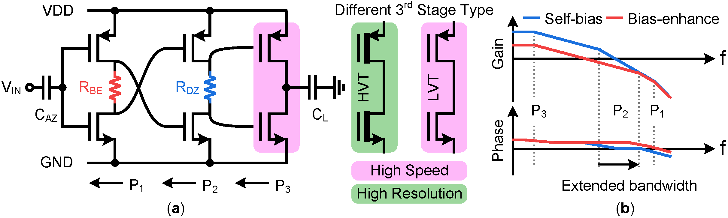
2. Ring Amplifier Review

With the evolution of the CMOS process, the design of traditional OTA, applied in amplifier-needed ADCs, is facing more and more challenges, such as the decrease of SNR due to the decrease of supply voltage and the decrease of intrinsic gain leading to non-negligible gain errors. Additionally, linearity is an important metric to consider during design [27,28]. A ringamp has been an attractive substitution for OTA, used as a residue amplifier (RA) in pipelined or pipelined-SAR ADCs, since the primary building block of a ringamp is its inverter [29]. Given its simple inverter-based structure, a ringamp can achieve a large slew-based charge current in large-signal settling phase, low power consumption, and near rail-to-rail output swing. More importantly, ringamps are more suitable for fine CMOS processes and have application scenarios in various types of ADCs due to the versatility of their structures. In the last decade, many ringamp-based ADC works [24,29,30,31,32,33,34,35,36,37,38,39] have appeared. Essentially, there are two different directions of the application, one for high resolution (signal-to-noise-and-distortion-ratio (SNDR) ≥ 70 dB) and the other for high speed (sampling rate fs ≥ 500 MHz), such as the dual-deadzone RAMP-based two-step SAR ADC [34], which achieves the highest SNDR for a ringamp-based high-resolution ADC, while [33] used a dead zone degeneration technique to realize the fastest sampling rate (fs = 1 GHz) for single-channel implementation.
A ringamp configured in closed-loop feedback typically produces as many poles as the number of inverters, and the dominated pole is located in the output node. Figure 2a shows the topology of a three-stage bias-enhanced ringamp with auto-zero and load capacitors. The self-biased ringamp [30] is replaced by a resistor R DZ inserted in the second stage to separate the signal without additional bias capacitors, enabling the transition of the ringamp from oscillation to amplification, due to the nature of the ringamp, which originates from a ring oscillator. The bias-enhanced ringamp is originally proposed in [31] by inserting a resistor R BE in the first stage and cross-coupling the top and bottom nodes of the resistors to the second stage. Due to the increase in the overdrive voltage of the second stage transistors, bias-enhanced ringamp can achieve larger bandwidth. Typically, for high-resolution applications, high-threshold voltage (HVT) transistors are preferred, in the third stage, to achieve high DC gain and operate in the cutoff region at a steady state, thus reducing ADC gain error and enabling calibration-free operation. Nevertheless, for high-speed application, the transistors in the third stage are typically low-threshold voltage (LVT) transistors to achieve high bandwidth and operate in the sub-threshold region at a steady state.
In this work, we have chosen the LVT transistor as the third stage, to achieve high bandwidth. We have improved the bias-enhanced ringamp with PVT compensation and fast-start circuits based on our previous work in [35]. Figure 2b shows the conceptual bode plot of this self-biased and bias-enhanced ringamp. There are three poles in the ringamp, expressed as
P s = 1 2 π R s C s
where s stands for the stage number and s {1, 2, 3}, R s and C s represent the small-signal resistance and total capacitor, considering the parasitic capacitor in the associated node. Normally, the values of poles meet P 3 P 2 P 1 . Due to the added resistor, R BE , in the first stage, the overdrive voltages for the second-stage transistors are increased, which leads to an extended bandwidth, assuming the other two poles remain the same, as Figure 2b shows. Although the loop gain is decreased a little, the bandwidth improvement is more essential for high-speed applications.

3. Proposed ADC Design

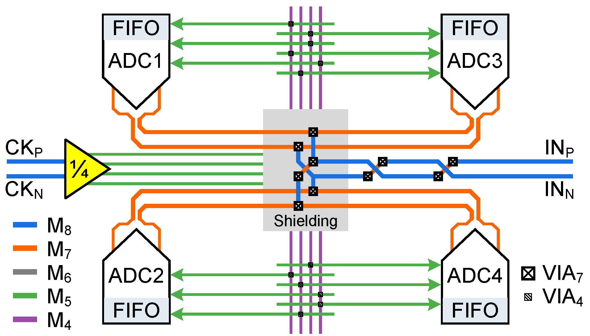
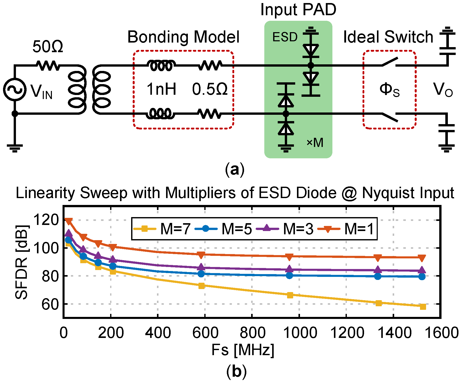
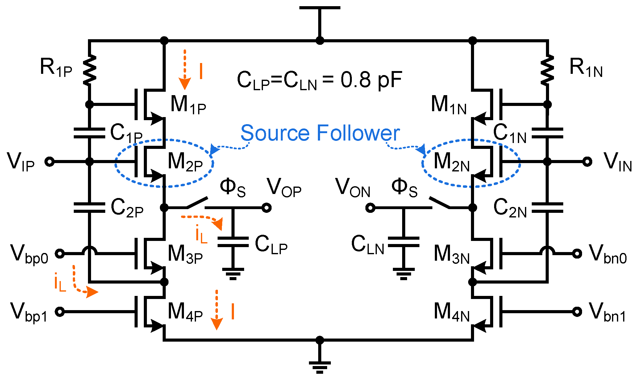
3.1. High-Linearity Front-End

The linearity of the high-speed ADC is deteriorated due to the bonding wire and non-linear capacitance of the diode at the input PAD for electro-static discharge (ESD) protection, especially when the input frequency increases. Figure 3a shows the extracted bonding parameters based on the ball grid array (BGA) package followed by the ideal sampling switch and capacitor. The number of ESD diodes is M for the simulations. The simulation result, as Figure 3b shows, is presented as the linearity versus the multiplier of the ESD diodes. The linearity decreases as the multiplier increase since the nonlinear diode capacitor is increased. However, the reliability increases with the number of diodes. In essence, it is a trade-off between linearity and stability. In this work, we choose M = 3 in this design to meet the linearity and reliability requirements.
To reduce the kickback noise and provide strong driving ability, an input buffer is required in high-speed ADC. Figure 4 shows the adopted replica capacitor-based source follower, maintaining a relatively constant current flowing the M 2 P / 2 N , thus providing high linearity. Additionally, to reduce the cross-talk between adjacent channels, the input buffer is embedded in the channel ADC as Section 3.2 shows.

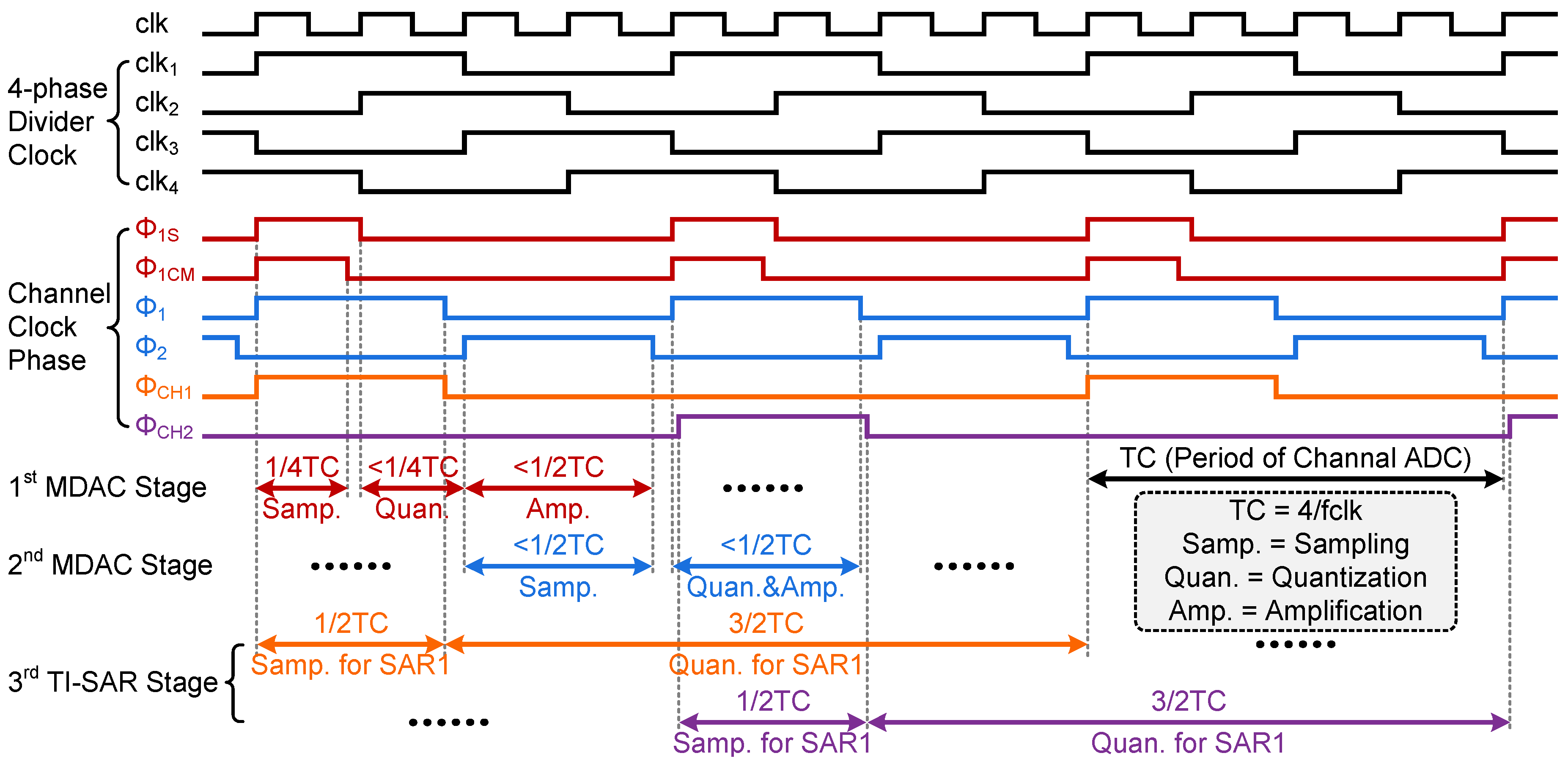
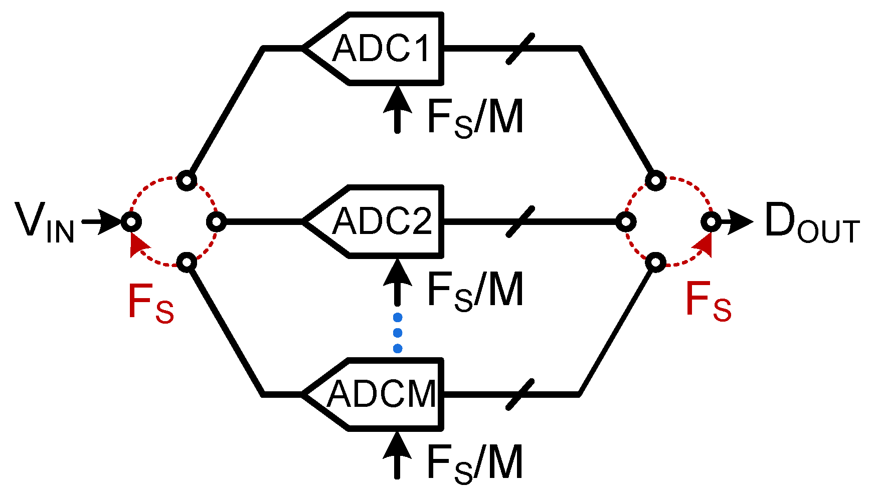
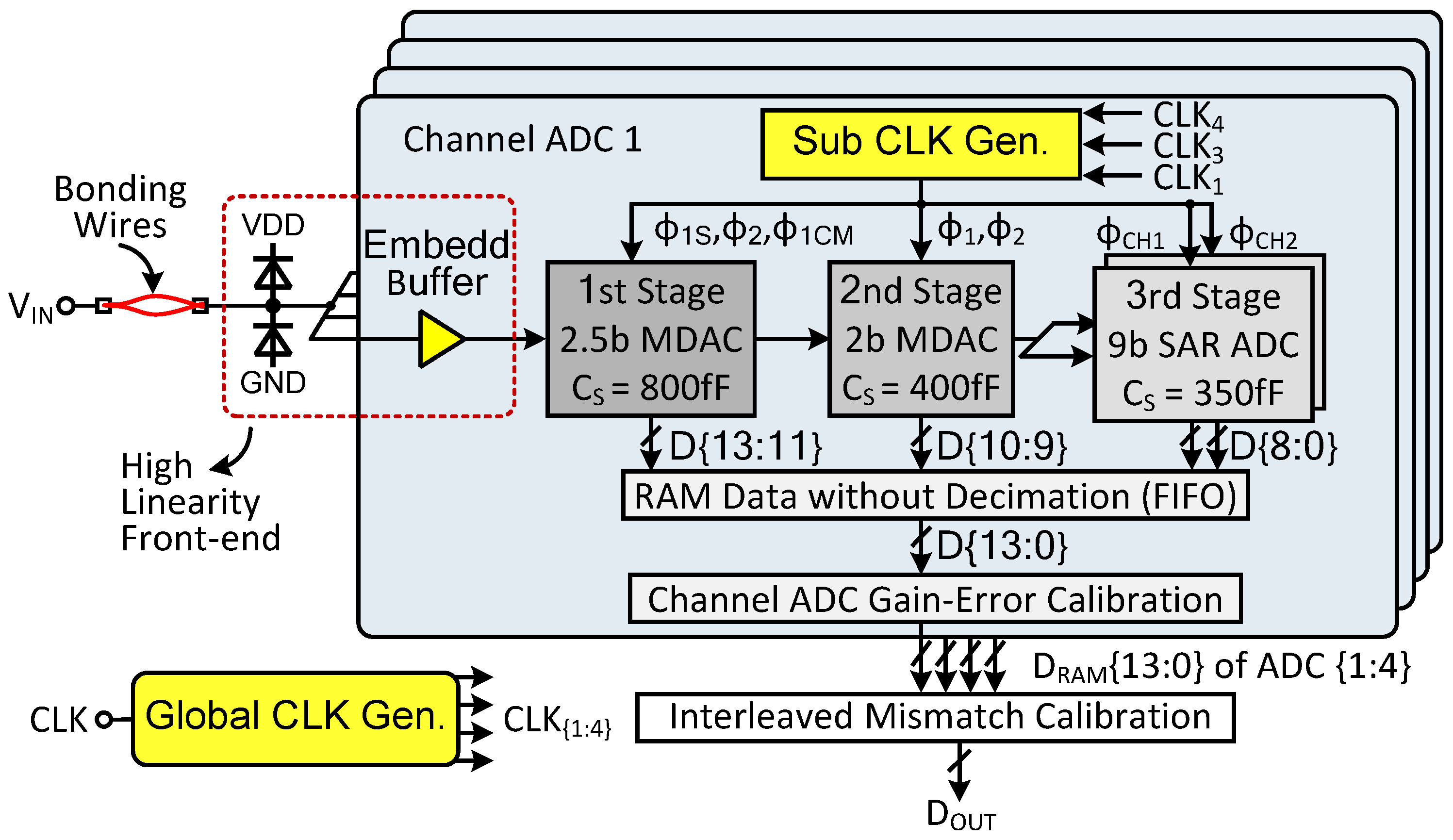
3.2. TI-ADC Architecture
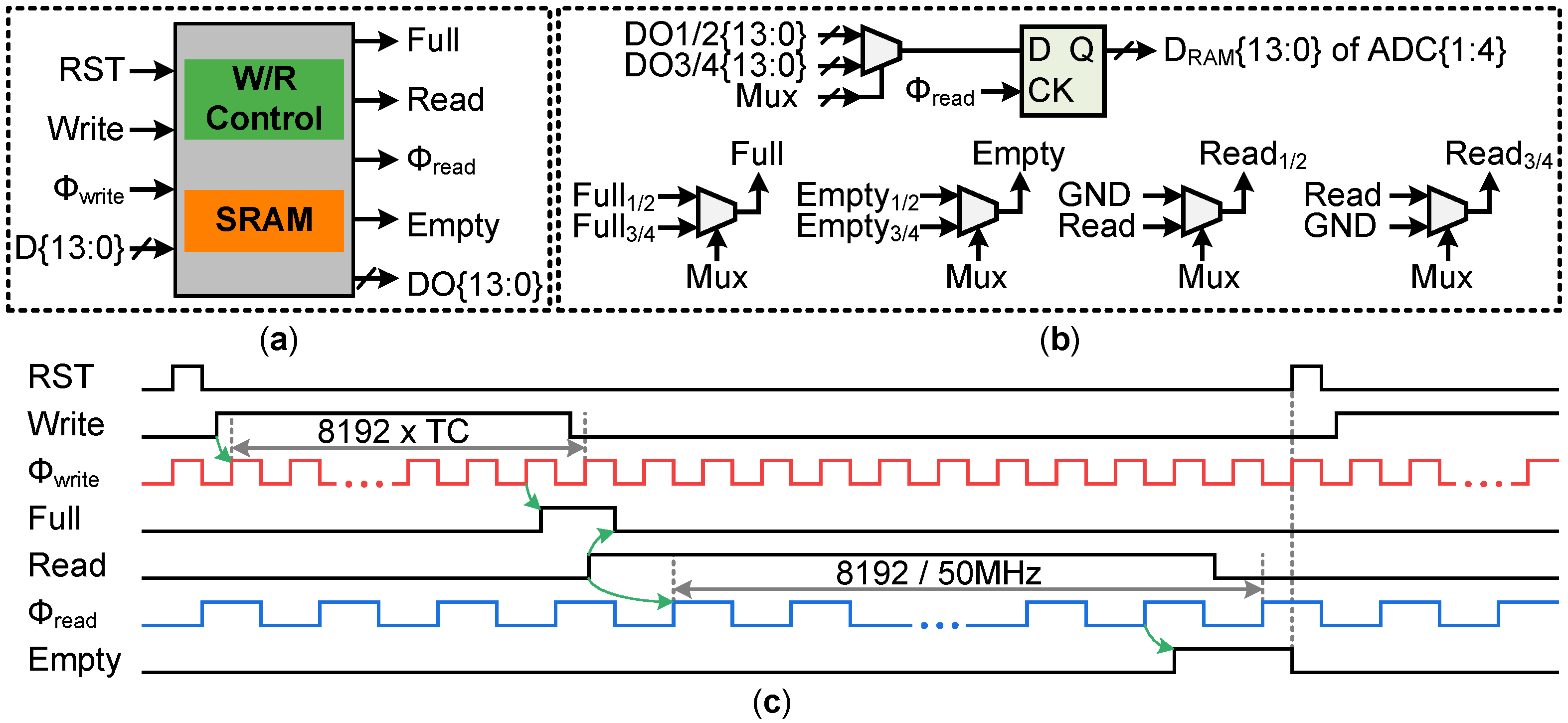
The architecture of SAR-assisted ringamp-based pipelined TI-ADC is illustrated in Figure 5. For the channel ADC, an SHA (sample-and-hold amplifier)-less architecture is adopted. Two MDAC (multiplying digital-to-analog converter) stages are adopted to achieve a high conversion rate, tackling 2.5-bit and 2-bit stages, respectively. For the last stage, which does not require an amplification phase, we use a two-channel time-interleaved asynchronous 9-bit SAR stage to achieve a high conversion rate as well as low power consumption. The 0.5-bit and 1-bit redundancies are adopted in the 1st and 2nd stages, respectively, to alleviate the requirement for comparators. The half-amplification structure used in the 2nd-stage further alleviates the requirement for the 2nd-stage amplifier. More details about the channel ADC can be obtained from [35]. The output data are captured by the on-chip RAM (FIFO, which will be explained in Section 3.3) without decimating the evaluation of the “real” performance of the channel ADC. A statistics-based calibration method is adopted, as in [35], to calibrate the nonlinear gain error of the ringamp for the channel ADC off-chip. After this, the mismatches of the TI-ADC are calibrated in the background, as discussed in Section 3.4 in the off-chip using Matlab.
The symmetrical differential input and clock routing structure is shown in Figure 6. The differential 2.5-GHz clock signal, CK P / N , generated from the clock generator, is divided by four to generate a four-phase 625-MHz clock to drive the four-channel sub-ADC. The differential input, IN P / N , is distributed as symmetrically as possible to avoid the even harmonics in the output spectrum. A shield plane is added for the area where the input and clock meet.
The timing diagram of the TI-ADC is shown in Figure 7. The TI-ADC is clocked from an external low-noise signal generator, and the four-phase divided clock after the global clock generator is distributed to the channel ADC symmetrically, as Figure 6 shows. The sampling time of the first stage accounts for 25 % of the clock period, T C , in channel ADC to increase the amplification time of the residue amplifier. For the second stage, the sampling time is 50 % , for an easy local clock generator. This two-way interleaved SAR stage achieves the required working speed.

3.3. FIFO Details

An embedded memory implemented in FIFO with a depth of 8K and a width of 16 bit is adopted is shown in Figure 8a. The FIFO is equipped with an asynchronous clock for r e a d and w r i t e , a reset signal, R S T , to clear the memory, and the f u l l and e m p t y signals to indicate the state of the FIFO. When the data is written, the f u l l signal is pulled high; then the data is read sequentially, first in, first out, and the f u l l signal is pulled low until the data is read. Figure 8b shows the sharing hardware between channel-1,3 and channel-2,4 for PAD saving. The timing diagram for the FIFO is demonstrated in Figure 8c.

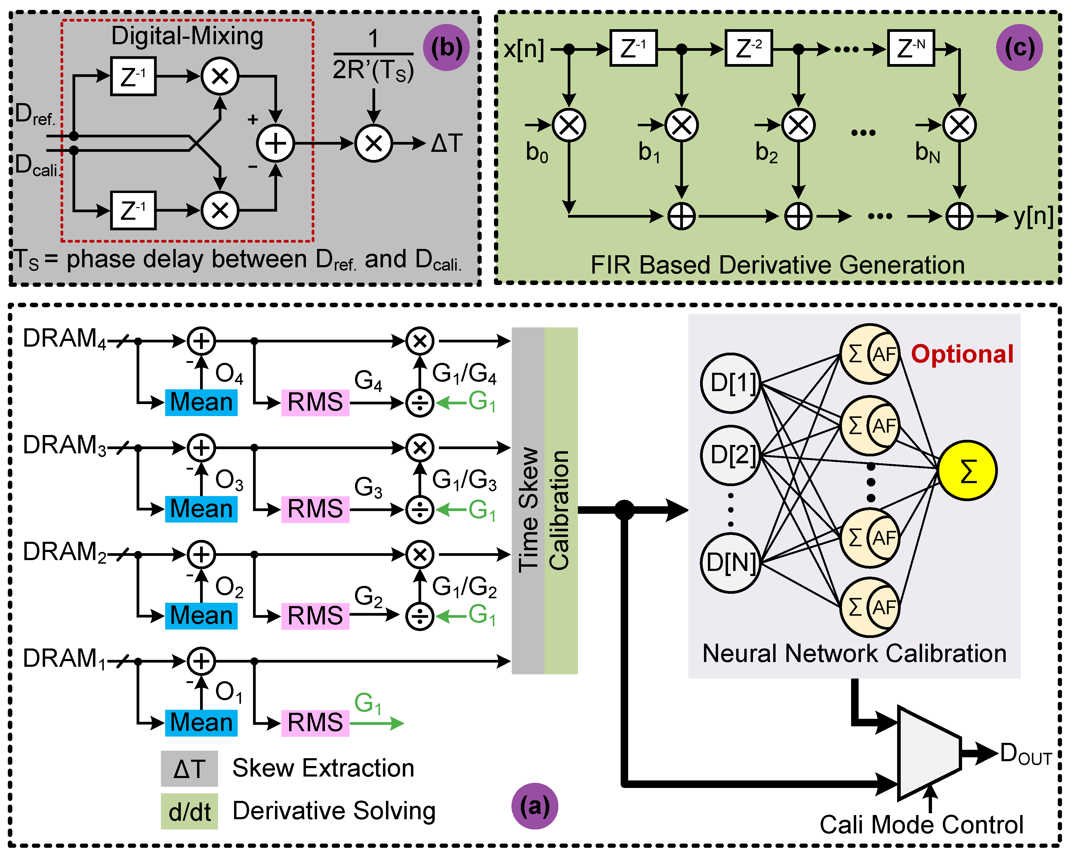
3.4. Digital Background Calibration

The blind digital background calibration flow is shown in Figure 9a. The offset and gain mismatches can be easily calibrated by averaging and gain normalization. First, each channel ADC removes the offset by subtracting the mean value of the channel code itself. Then, the gain mismatch is calibrated by normalizing the gain factor to the reference channel (ADC1 in this design).
The timing mismatch is calibrated using digital mixing [16]. Based on the autocorrelation function, the timing skew Δ T can be calculated as
Δ T = D Δ T ¯ 2 d R x d τ | τ = T C K
where R x is the autocorrelation function of input, and D Δ T ¯ is the output of the digital mixing (as shown in Figure 9b) between the under-calibrated and reference channels. After getting the timing skew, the calibrated output is
D c a l = D u n c a l D u n c a l × Δ T .
The focal point is to obtain the derivative of the input signal. It is realized using an FIR filter, as shown in Figure 9c in Matlab. The timing skew mismatch calibration sequence behaves in a “middle-search” way. First, the channel 1 data is used to calibrate channel 3. Next, the calibrated channels 3 and 1 are used to calibrate channels 2 and 4. Finally, the calibrated 4-channel data are merged to the final output of the TI-ADC. An optional neural network calibration (NNC) is also included [40]. The measurement results with and without NNC are shown in Section 4.

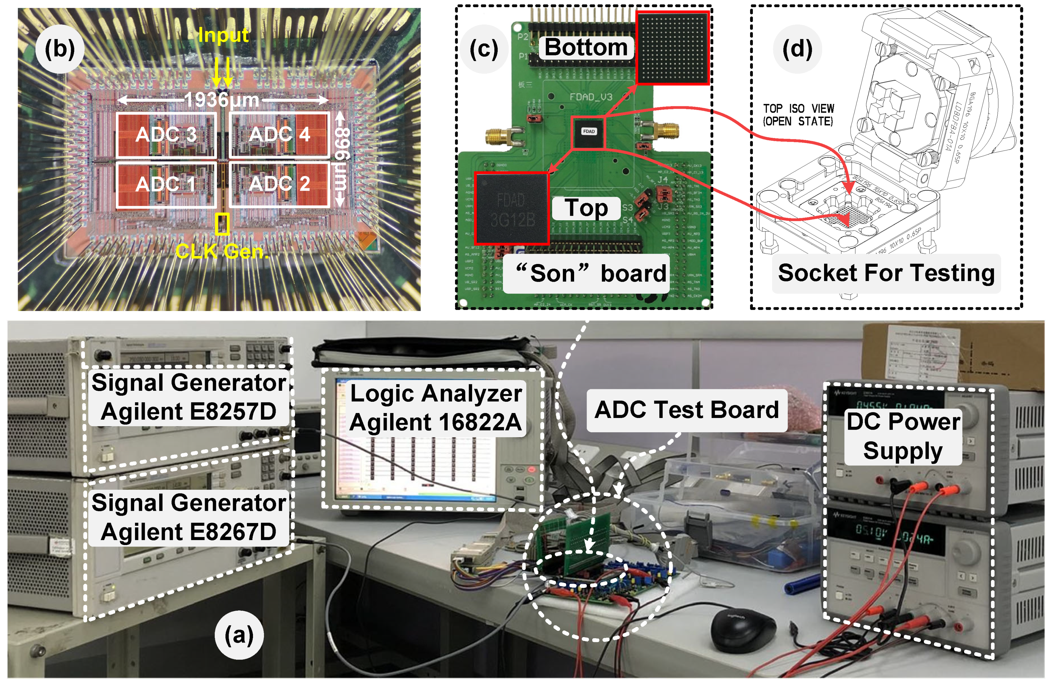
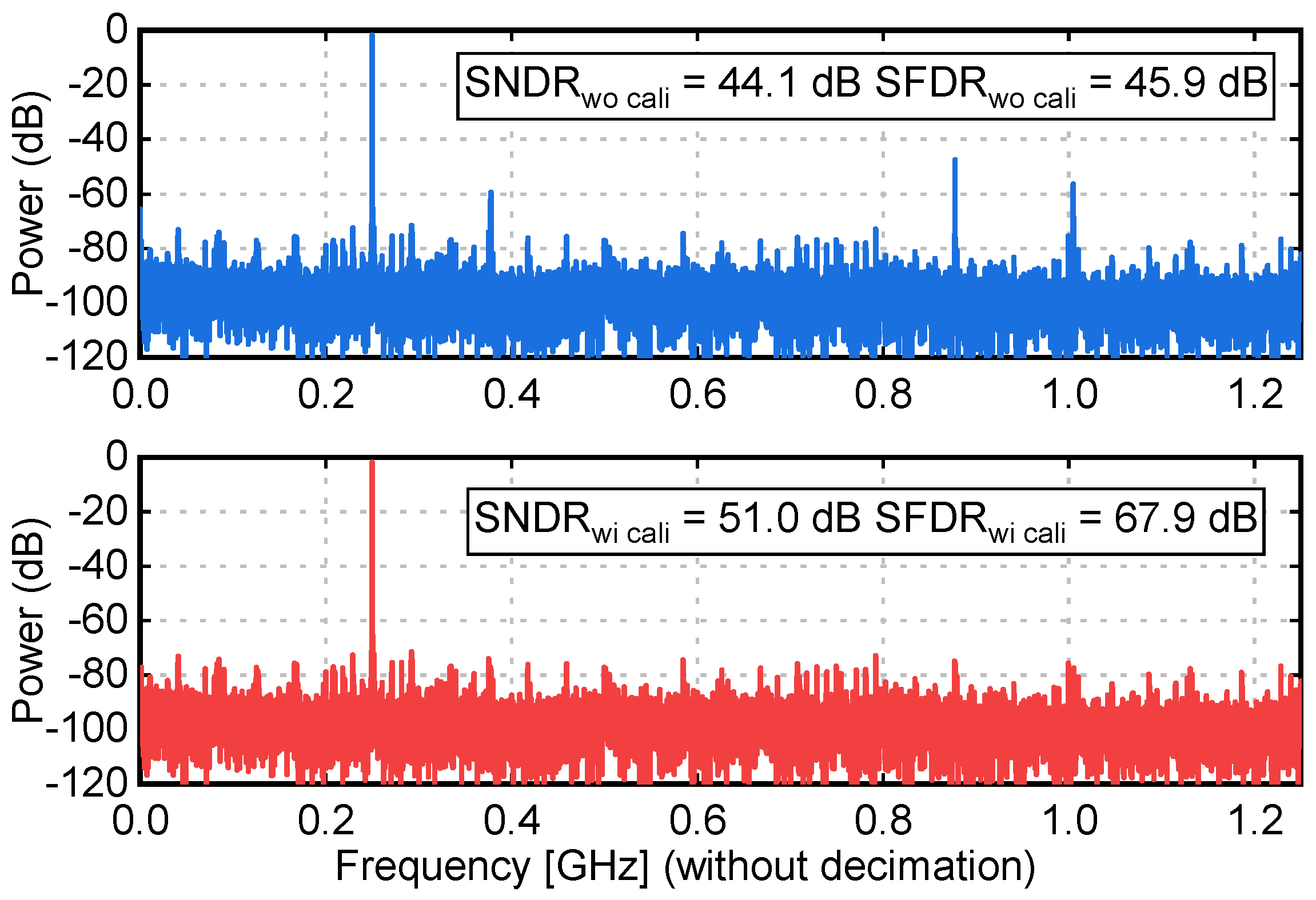
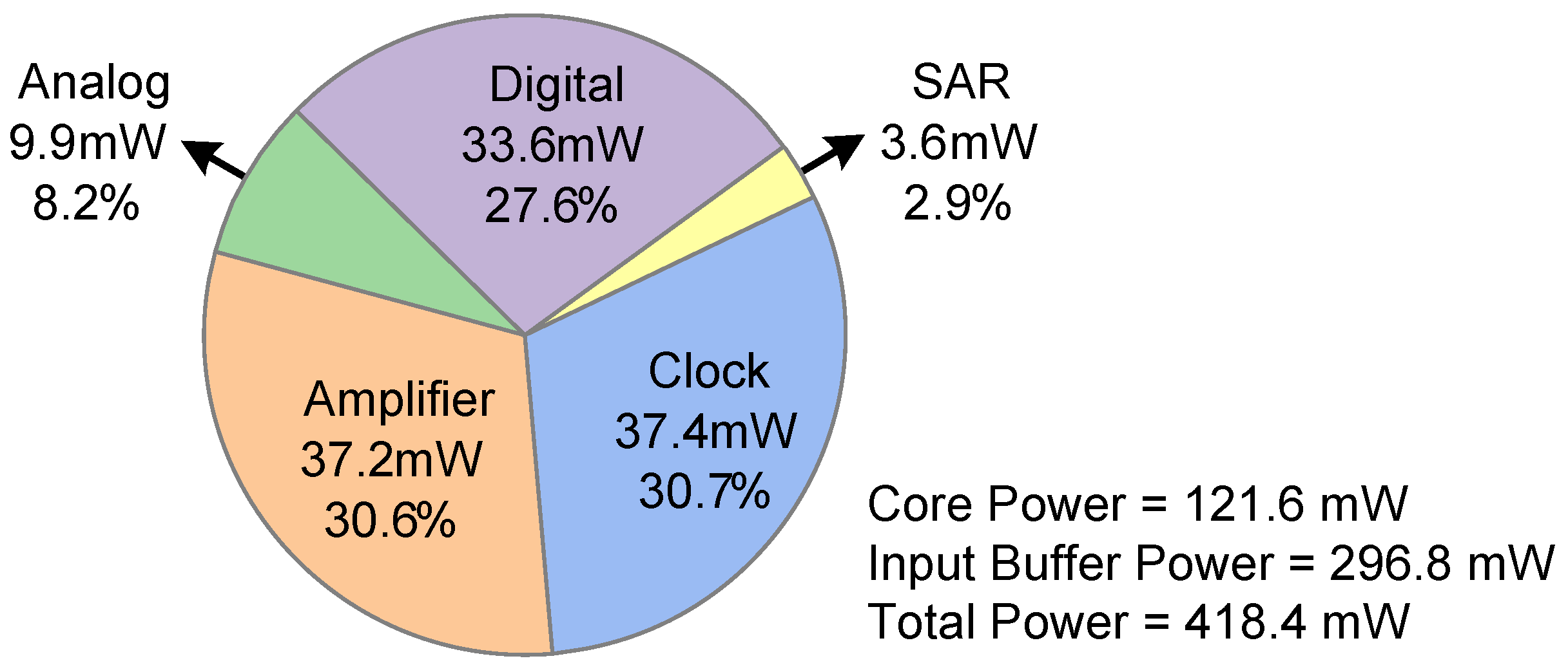
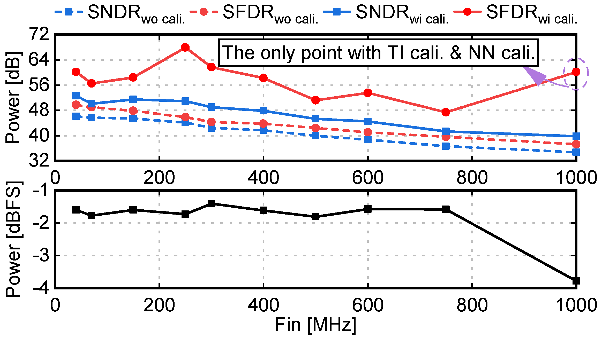
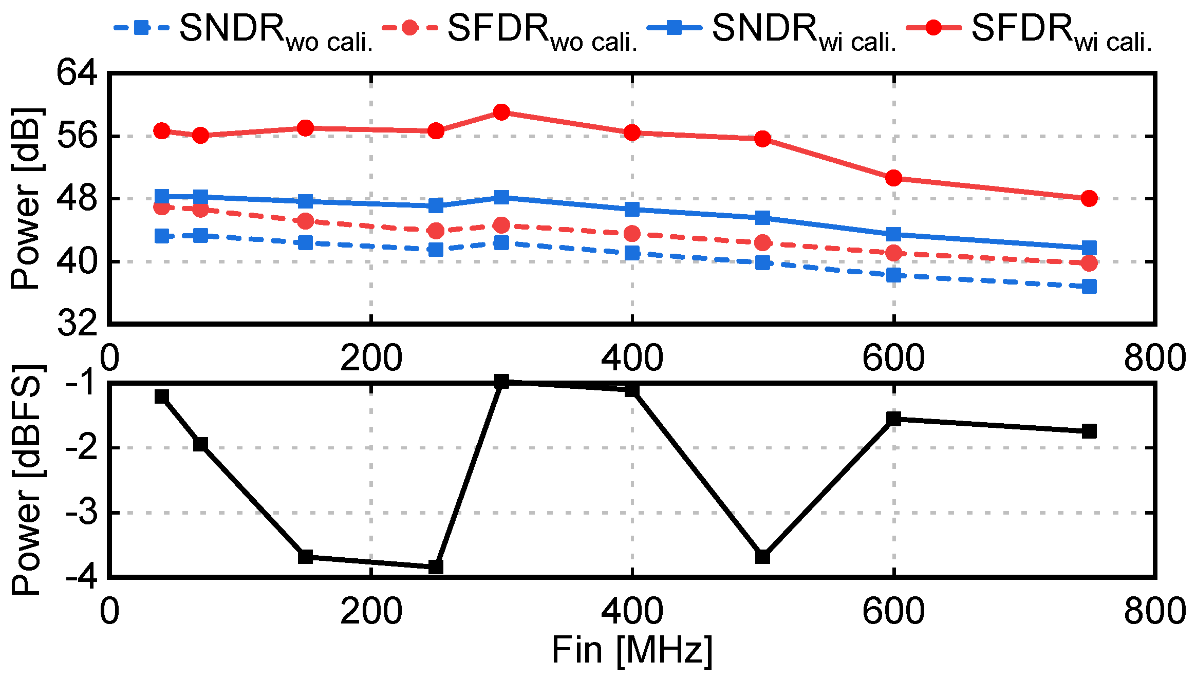
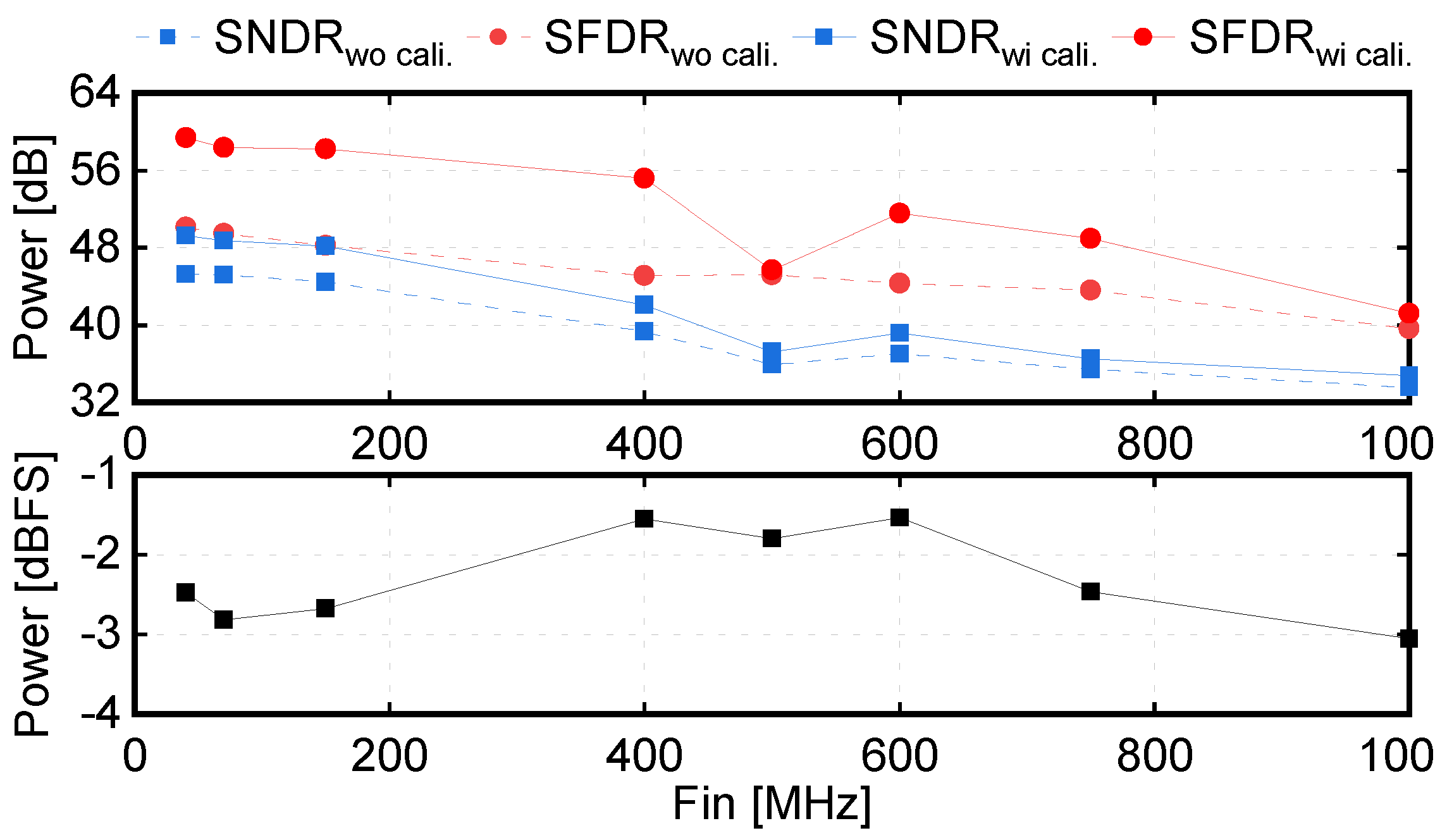
4. Measurement Results

The prototype 12-bit ADC is designed with the standard 28-nm CMOS technology. The measurement setup for evaluating the ADC performance is shown in Figure 10a. The input signal is generated from a signal source (Agilent E8267D), followed by a band-pass filter with a center frequency equal to the input frequency (not shown in the figure) to guarantee the spectrum purity. The low-phase-noise clock is generated by a signal source (Agilent E8257D). Three separate power supplies for high-voltage input buffer (2.0 and −0.5-V), high-noise digital power (1.0-V), and low-noise analog power (1.0-V) are provided by the low-dropout regulator on the printed circuit board (PCB). The FIFO data are read by an Agilent logic analyzer 16822A with control signals to meet the timing diagram of the FIFO. The captured data are reconstructed and calibrated on a host PC. Figure 10b shows a microphotograph, wherein the core occupies an area of 1936 μ m × 896 μ m, and the remaining chip area is filled with the decoupling capacitor and pads. The global clock generator is located in the lower center, and the divided output clocks are symmetrically distributed to the channel ADC. The input signal is poured from the upper center pads. To reduce the bonding wire ringing effect, double or triple bonding is adopted in the pad layout and package scheme. Figure 10c shows the “son” board of the PCB and the BGA-196 package chip. To improve the measurement efficiency, a socket for testing is customized, as shown in Figure 10d.
At a 2.5-GS/s working speed under a 1.0-V power supply for the core ADC and 2.0/−0.5-V for the high-linearity input buffer, the total power consumption is 418.4 mW. The core power breakdown is shown in Figure 11. The embedded input buffer in the high-voltage domain accounts for 70 % of the total TI-ADC power consumption, where the power of a single buffer is 64.2 mW and the left power is used for the impedance matching. The residue amplifier accounts for only 30.6 % of the core power, which is the main advantage of this ringamp-based pielined-SAR ADC. The measured DNL and INL after calibration are +1.75/−1.00 LSB and +3.31/−2.98 LSB, respectively.
The measured FFT spectrum of the proposed TI-ADC with near −1 dBFS input power @ 2.5 GS/s for a 250-MHz input with and without calibration are shown in Figure 12 (NNC is not used). Unless stated otherwise, all measurement results are reported for a sampling rate of 2.5 GHz. After the digital background calibration, the offset, gain, and timing-mismatch spurs are all below −70 dBFS, which will not limit the overall TI-ADC linearity performance. The SNDR improves to 51.0 dB, while the uncalibrated value is only 44.1 dB. The SFDR improves 22 dB without any interleaved spur in the calibrated output spectrum.
The measured FFT spectrum of the proposed TI-ADC @ 2.5 GS/s for a 1-GHz input with digital background calibration and additional NNC are shown in Figure 13. After the digital background calibration, the offset, gain, and timing mismatches spurs are all below −70 dBFS, and the linearity performance is not limited by the interleaved spurs. The performance degradation is mainly due to the large noise (low SNR), especially the clock-jitter noise, which can be verified from the spectrum. The large internal clock jitter is calculated around 650 fs by comparing the low- and high-input frequency SNR performance.
The SFDR improves to 60.1 dB with the NNC turned on, while the value with digital calibration is only 51.7 dB. To summarize, the NNC can improve the linearity performance, however, it does not help the SNR improvement, since the SNR is limited by the circuity-level noise.
Figure 14 shows the dynamic performance measured with various input frequencies @ a 2.5 GS/s working rate. Due to the limited power of the signal generator in the laboratory, the input power at 1 GHz is reduced to near 4 dBFS. The results verify the effectiveness of the blind digital background calibration. The deterioration of the performance at high input frequency is mainly caused by the large internal clock jitter around 650 fs and less decoupling of the capacitor for the clock generator to suppress the supply ripple for the clock buffer. The main linearity at high input frequency is caused by the second harmonic due to the imbalance in the test printed circuit board (PCB) routing between the differential input. Additionally, the long routing from the mother-board to the real test “son-board” generated additional noise during ADC measurement. Since the high-output raw data are captured by the on-chip RAM and are read out without any decimation, the output performance will not benefit from the decimation as traditional works have.
Figure 15 shows the dynamic performance measured with various input frequencies @ a 2.0-GS/s working rate. The SFDR improves more than 8 dB for a wide range of input frequencies with the background calibration. Figure 16 shows the dynamic performance measured with various input frequencies @ a 3.0-GS/s working rate. The improvement is less at a high working rate because of the incomplete settling of the ringamp, especially at the high input frequency.
Figure 14. Measured dynamic performance versus input frequency @ 2.5 GS/s and associated input power. (The performance for the 1-GHz input frequency is further calibrated with a NNC, other measurements are based on interleaved mismatches calibration only including Figure 16).
Electronics 10 03173 g014
Figure 15. Measured dynamic performance versus input frequency @ 2.0 GS/s and associated input power.
Electronics 10 03173 g015
Figure 16. Measured dynamic performance versus input frequency @ 3.0 GS/s and associated input power.
Electronics 10 03173 g016
Table 1 summarizes the measured performance compared with the recently published high-speed TI-ADCs. It explors the pipelined-SAR architecture as the channel ADC for the TI-ADC; due to the large power consumption of the input buffer, the total power is not reduced significantly. However, the power of the total ADC is still competitive. The ADC achieves a FoM w of 0.48 pJ/conv.-step at a 250-MHz input.

5. Conclusions

This paper proposed a ringamp-based pipelined-SAR four-channel TI-ADC. To achieve high linearity, a modified input PAD with a decreased number of ESD diodeswas adopted, which maintained adequate protection. The input buffer with replica load was used to reduce the kickback noise at high input frequency and to maintain high linearity. Additionally, a digital-mixing-based blind background calibration method was used to alleviate the detrimental effects of mismatches among the interleaved channels. An optional NNC was also adopted to achieve high linearity at the high-input frequency. Measured at 2.5 GS/s, the ADC achieved a low-frequency SNDR/SFDR of 51.0/68.0 dB, translating to a competitive FoM w of 0.48 pJ/conv.-step at 250-MHz input.

Author Contributions

Research methodology, Y.C., Z.N.; Circuits design, J.L., X.S., Y.C., Z.N.; Layout drawing, J.L., X.S., Y.C., Z.N.; Writing—original draft preparation, J.L., F.Y.; Supervision, J.R.; Validation, J.L., D.Z., X.S., Y.C., Z.N. All authors have read and agreed to the published version of the manuscript.

Funding

This paper is sponsored by National Natural Science Foundation of China with No. 62074038.

Data Availability Statement

Data is contained within the article. The data presented in this study are available in this paper.

Acknowledgments

The authors would like to thank Shuai Li from State Key Laboratory of ASIC & System, Fudan University for ADC measurement supporting.

Conflicts of Interest

The authors declare no conflict of interest.

Abbreviations

The following abbreviations are used in this manuscript:
CMOSComplementary metal oxide silicon
ADCAnalog-to-digital converter
DACDigital-to-analog converter
GS/sGiga samples per second
HVTHigh threshold voltage
LVTLow threshold voltage
ESDElectro-static discharge
BGABall grid array
SHASample and hold amplifier
RAResidue amplifier
RingampRing amplifier
SARSuccessive-approximation register
TITime interleaved
NNCNeural Network Calibration
FFTFast Fourier transform
FIRFinite impulse response
FOMFigure of merit
LDOLow dropout regulator
MDACMultiplying digital-to-analog converter
SNDRSignal-to-noise-and-distortion ratio
SFDRSpurious free dynamic range
FIFOFirst input first output
PCBPrinted circuit board

References

  1. Brandolini, M.; Shin, Y.J.; Raviprakash, K.; Wang, T.; Wu, R.; Geddada, H.M.; Ko, Y.; Ding, Y.; Huang, C.; Shih, W.; et al. A 5 GS/s 150 mW 10 b SHA-Less Pipelined/SAR Hybrid ADC for Direct-Sampling Systems in 28 nm CMOS. IEEE J. Solid-State Circuits 2015, 50, 2922–2934. [Google Scholar] [CrossRef]
  2. Swindlehurst, E.; Jensen, H.; Petrie, A.; Song, Y.; Kuan, Y.C.; Qu, Y.; Chang, M.C.F.; Wu, J.T.; Chiang, S.H.W. An 8-bit 10-ghz 21-mw time-interleaved sar adc with grouped dac capacitors and dual-path bootstrapped switch. IEEE J. Solid-State Circuits 2021, 56, 2347–2359. [Google Scholar] [CrossRef]
  3. Chang, D.J.; Choi, M.; Ryu, S.T. A 28-nm 10-b 2.2-GS/s 18.2-mW Relative-Prime Time-Interleaved Sub-Ranging SAR ADC With On-Chip Background Skew Calibration. IEEE J. Solid-State Circuits 2021, 56, 2691–2700. [Google Scholar] [CrossRef]
  4. Guo, M.; Mao, J.; Sin, S.W.; Wei, H.; Martins, R.P. A 1.6-GS/s 12.2-mW seven-/eight-way split time-interleaved SAR ADC achieving 54.2-dB SNDR with digital background timing mismatch calibration. IEEE J. Solid-State Circuits 2019, 55, 693–705. [Google Scholar] [CrossRef]
  5. Yu, B.; Chen, C.; Ye, F.; Ren, J. A mixed sample-time error calibration technique in time-interleaved ADCs. IEICE Electron. Express 2013, 10, 1–11. [Google Scholar] [CrossRef] [Green Version]
  6. Wei, H.; Zhang, P.; Sahoo, B.D.; Razavi, B. An 8 Bit 4 GS/s 120 mW CMOS ADC. IEEE J. Solid-State Circuits 2014, 49, 1751–1761. [Google Scholar] [CrossRef]
  7. Ku, I.-N.; Xu, Z.; Kuan, Y.-C.; Wang, Y.-H.; Chang, M.-C.F. A 40-mW 7-bit 2.2-GS/s time-interleaved subranging CMOS ADC for low-power gigabit wireless communications. IEEE J. Solid-State Circuits 2012, 47, 1854–1865. [Google Scholar] [CrossRef]
  8. Wu, J.; Chou, A.; Yang, C.-H.; Ding, Y.; Ko, Y.-J.; Lin, S.-T.; Liu, W.; Hsiao, C.-M.; Hsieh, M.-H.; Huang, C.-C.; et al. A 5.4GS/s 12b 500mW Pipeline ADC in 28nm CMOS. In Proceedings of the 2013 Symposium on VLSI Circuits, Kyoto, Japan, 16 August 2013; pp. C92–C93. [Google Scholar]
  9. Singh, S.; Anttila, L.; Epp, M.; Schlecker, W.; Valkama, M. Frequency Response Mismatches in 4-channel Time-Interleaved ADCs: Analysis, Blind Identification, and Correction. IEEE Trans. Circuits Syst. I Regul. Pap. 2015, 62, 2268–2279. [Google Scholar] [CrossRef]
  10. Zhou, Y.; Xu, B.; Chiu, Y. A 12-b 1-GS/s 31.5-mW Time-Interleaved SAR ADC With Analog HPF-Assisted Skew Calibration and Randomly Sampling Reference ADC. IEEE J. Solid-State Circuits 2019, 54, 2207–2218. [Google Scholar] [CrossRef]
  11. Yin, M.; Ye, Z. First order statistic based fast blind calibration of time skews for time-interleaved ADCs. IEEE Trans. Circuits Syst. II Express Briefs 2020, 67, 162–166. [Google Scholar] [CrossRef]
  12. Razavi, B. Design considerations for interleaved ADCs. IEEE J. Solid-State Circuits 2013, 48, 1806–1817. [Google Scholar] [CrossRef] [Green Version]
  13. Wang, X.; Li, F.; Jia, W.; Wang, Z. A 14-bit 500-MS/s time-interleaved ADC with autocorrelation-based time skew calibration. IEEE Trans. Circuits Syst. II Express Briefs 2018, 66, 322–326. [Google Scholar] [CrossRef]
  14. Lin, C.-Y.; Wei, Y.-H.; Lee, T.-C. A 10-bit 2.6-GS/s time-interleaved SAR ADC with a digital-mixing timing-skew calibration technique. IEEE J. Solid-State Circuits 2018, 53, 1508–1517. [Google Scholar] [CrossRef]
  15. Le Dortz, N.; Blanc, J.P.; Simon, T.; Verhaeren, S.; Rouat, E.; Urard, P.; Le Tual, S.; Goguet, D.; Lelandais-Perrault, C.; Benabes, P. A 1.62 GS/s time-interleaved SAR ADC with digital background mismatch calibration achieving interleaving spurs below 70 dBFS. In Proceedings of the IEEE International Solid-State Circuits Conference, San Francisco, CA, USA, 9–13 February 2014; pp. 386–388. [Google Scholar]
  16. Guo, M.; Mao, J.; Sin, S.W.; Wei, H.; Martins, R.P. A 29mW 5GS/s Time-interleaved SAR ADC achieving 48.5dB SNDR With Fully-Digital Timing-Skew Calibration Based on Digital-Mixing. In Proceedings of the IEEE Symposium on VLSI Circuits Digest of Technical Papers, Kyoto, Japan, 5–8 June 2017; pp. C76–C77. [Google Scholar]
  17. Janssen, E.; Doris, K.; Zanikopoulos, A.; Murroni, A.; Van Der Weide, G.; Lin, Y.; Alvado, L.; Darthenay, F.; Fregeais, Y. An 11b 3.6 GS/s time-interleaved SAR ADC in 65nm CMOS. In Proceedings of the IEEE International Solid-State Circuits Conference, San Francisco, CA, USA, 17–21 February 2013; pp. 464–465. [Google Scholar]
  18. Doris, K.; Janssen, E.; Nani, C.; Zanikopoulos, A.; Van Der Weide, G. A 480 mW 2.6 GS/s 10b Time-Interleaved ADC With 48.5 dB SNDR up to Nyquist in 65 nm CMOS. IEEE J. Solid-State Circuits 2011, 46, 2821–2833. [Google Scholar] [CrossRef]
  19. Jia, H.; Guo, X.; Wu, D.; Zhou, L.; Luan, J.; Wu, N.; Huang, Y.; Zheng, X.; Wu, J.; Liu, X. A 12-Bit 2.4 GS/s Four-Channel Pipelined ADC with a Novel On-Chip Timing Mismatch Calibration. Electronics 2020, 9, 910. [Google Scholar] [CrossRef]
  20. Chen, C.Y.; Wu, J.; Hung, J.J.; Li, T.; Liu, W.; Shih, W.T. A 12-bit 3 GS/s pipeline ADC with 0.4 mm 2 and 500 mW in 40 nm digital CMOS. IEEE J. Solid-State Circuits 2012, 47, 1013–1021. [Google Scholar] [CrossRef]
  21. Li, J.; Guo, X.; Luan, J.; Wu, D.; Zhou, L.; Huang, Y.; Wu, N.; Jia, H.; Zheng, X.; Wu, J.; et al. A 3GSps 12-bit four-channel time-interleaved pipelined ADC in 40 nm CMOS process. Electronics 2019, 8, 1551. [Google Scholar] [CrossRef] [Green Version]
  22. Ramkaj, A.T.; Ramos, J.C.P.; Pelgrom, M.J.; Steyaert, M.S.; Verhelst, M.; Tavernier, F. A 5-GS/s 158.6-mW 9.4-ENOB passive-sampling time-interleaved three-stage pipelined-SAR ADC with Analog–Digital corrections in 28-nm CMOS. IEEE J. Solid-State Circuits 2020, 55, 1553–1564. [Google Scholar] [CrossRef]
  23. Ali, A.M.; Dinc, H.; Bhoraskar, P.; Dillon, C.; Puckett, S.; Gray, B.; Speir, C.; Lanford, J.; Brunsilius, J.; Derounian, P.R.; et al. A 14 bit 1 GS/s RF sampling pipelined ADC with background calibration. IEEE J. Solid-State Circuits 2014, 49, 2857–2867. [Google Scholar] [CrossRef]
  24. Hershberg, B.; Dermit, D.; Liempd, B.; Martens, E.; Markulic, N.; Lagos, J.; Craninckx, J. A 3.2 GS/s 10 ENOB 61mW ringamp ADC in 16 nm with background monitoring of distortion. In Proceedings of the IEEE International Solid-State Circuits Conference, San Francisco, CA, USA, 17–21 February 2019. [Google Scholar]
  25. Verma, D.; Shehzad, K.; Khan, D.; Kim, S.J.; Pu, Y.G.; Yoo, S.S.; Hwang, K.C.; Yang, Y.; Lee, K.Y. A Design of Low-Power 10-bit 1-MS/s Asynchronous SAR ADC for DSRC Application. Electronics 2020, 9, 1100. [Google Scholar] [CrossRef]
  26. Aiello, O.; Crovetti, P.; Alioto, M. Fully synthesizable low-area analogue-to-digital converters with minimal design effort based on the dyadic digital pulse modulation. IEEE Access 2020, 8, 70890–70899. [Google Scholar] [CrossRef]
  27. Wan, P.; Su, L.; Zhang, H.; Chen, Z. A Power-Efficient Pipelined ADC with an Inherent Linear 1-Bit Flip-Around DAC. Electronics 2020, 9, 199. [Google Scholar] [CrossRef] [Green Version]
  28. Choi, M.Y.; Kong, B.S. Linearity Enhancement of VCO-Based Continuous-Time Delta-Sigma ADCs Using Digital Feedback Residue Quantization. Electronics 2021, 10, 2773. [Google Scholar] [CrossRef]
  29. Hershberg, B.; Weaver, S.; Sobue, K.; Takeuchi, S.; Hamashita, K.; Moon, U.-K. Ring Amplifiers for Switched Capacitor Circuits. IEEE J. Solid-State Circuits 2012, 47, 2928–2942. [Google Scholar] [CrossRef] [Green Version]
  30. Lim, Y.; Flynn, M. A 100 MS/s 10.5 b 2.46 mW comparator-less pipeline ADC using self-biased ring amplifiers. In Proceedings of the IEEE International Solid-State Circuits Conference Digest of Technical Paper, San Francisco, CA, USA, 9–13 February 2014. [Google Scholar]
  31. Chen, Y.; Wang, J.; Hu, H.; Ye, F.; Ren, J. A 200 MS/s, 11 bit SAR-assisted pipeline ADC with bias-enhanced ring amplifier. In Proceedings of the IEEE International Symposium on Circuits and Systems, Baltimore, MD, USA, 28–31 May 2017. [Google Scholar]
  32. Lee, C.; Venkatachala, P.; ElSHater, A.; Xiao, B.; Hu, H.; Moon, U. Cascoded ring amplifiers for high speed and high accuracy settling. In Proceedings of the IEEE International Symposium on Circuits and Systems, Sapporo, Japan, 26–29 May 2019. [Google Scholar]
  33. Lagos, J.; Hershberg, B.; Martens, E.; Wambacq, P.; Craninckx, J. A 1-GS/s, 12-b, Single-Channel Pipelined ADC With Dead-Zone-Degenerated Ring Amplifiers. IEEE J. Solid-State Circuits 2019, 54, 646–658. [Google Scholar] [CrossRef]
  34. Elshater, A.; Venkatachala, P.K.; Lee, C.Y.; Muhlestein, J.; Leuenberger, S.; Sobue, K.; Hamashita, K.; Moon, U.-K. A 10-mW 16-b 15-MS/s Two-Step SAR ADC With 95-dB DR Using Dual-Deadzone Ring Amplifier. IEEE J. Solid-State Circuits 2019, 54, 3410–3420. [Google Scholar] [CrossRef]
  35. Lan, J.; Chen, Y.; Shen, X.; Ni, Z.; Wu, Y.; Ye, F.; Ren, J. Effective Gain Analysis and Statistic Based Calibration for Ring Amplifier with Robustness to PVT Variation. IEEE Trans. Circuits Syst. II Express Briefs 2021. early access. [Google Scholar] [CrossRef]
  36. Lee, J.; Lee, S.; Kim, K.; Chae, H. A Pipelined Noise-Shaping SAR ADC Using Ring Amplifier. Electronics 2021, 10, 1968. [Google Scholar] [CrossRef]
  37. Lagos, J.; Markulic, N.; Hershberg, B.; Dermit, D.; Shrivas, M.; Martens, E.; Craninckx, J. A 10.0 ENOB, 6.2 fJ/conv.-step, 500 MS/s Ringamp-Based Pipelined-SAR ADC with Background Calibration and Dynamic Reference Regulation in 16nm CMOS. In Proceedings of the 2013 Symposium on VLSI Circuits, Kyoto, Japan, 13–19 June 2021; pp. 1–2. [Google Scholar]
  38. Megawer, K.M.; Hussien, F.A.; Aboudina, M.M.; Mohieldin, A.N. A Systematic Design Methodology for Class-AB-Style Ring Amplifiers. IEEE Trans. Circuits Syst. II Express Briefs 2018, 65, 1169–1173. [Google Scholar] [CrossRef]
  39. Conrad, J.; Vogelmann, P.; Mokhtar, M.A.; Ortmanns, M. Design Approach for Ring Amplifiers. IEEE Trans. Circuits Syst. I Regul. Pap. 2015, 67, 3444–3457. [Google Scholar] [CrossRef]
  40. Zhang, T.; Cao, Y.; Zhang, S.; Chen, C.; Ye, F.; Ren, J. Machine learning based prior-knowledge-free calibration for split pipelined-SAR ADCs with open-loop amplifiers achieving 93.7-dB SFDR. In Proceedings of the IEEE 45th European Solid State Circuits Conference, Krakow, Poland, 23–26 September 2019; pp. 189–192. [Google Scholar]
Figure 1. Conceptual block diagram of TI-ADC.
Electronics 10 03173 g001
Figure 2. Proposed bias-enhanced ring amplifier for high-speed ADC: (a) The schematic of the basic three-stage ringamp and the different configuration in the 3rd stage for various applications; (b) The conceptual bode plot to explain the bandwidth extension by the proposed bias-enhanced ringamp.
Electronics 10 03173 g002
Figure 3. High linearity modified input pad and simulated result: (a) The simulation setup to evaluate the linearity of the front-end considering the parasitic model of packaging and ESD diodes; (b) The simulation results of linearity versus multipliers of ESD diodes.
Electronics 10 03173 g003
Figure 4. The differential input buffer.
Electronics 10 03173 g004
Figure 5. Top-level 2.5 GS/s 12-b four-way TI-ADC architecture (single-ended, actually differential).
Electronics 10 03173 g005
Figure 6. Input and clock routing details.
Electronics 10 03173 g006
Figure 7. Timing diagram of the TI-ADC.
Electronics 10 03173 g007
Figure 8. FIFO details: (a) Functional block diagram; (b) The data selecting and sharing hardware for the adjacent channels; (c) The timing diagram for the FIFO.
Electronics 10 03173 g008
Figure 9. Digital background calibration for offset, gain, and timing mismatch: (a) The complete TI mismatches calibration with NNC optional; (b) Skew extraction based on digital-mixing; (c) Derivative solving based on FIR filter.
Electronics 10 03173 g009
Figure 10. Chip microphotograph and measurement details: (a) The measurement setup for the 4-way TI-ADC; (b) Chip microphotograph; (c) The “son” board and associated BGA package; (d) The socket for the BGA testing.
Electronics 10 03173 g010
Figure 11. Measured core power breakdown.
Electronics 10 03173 g011
Figure 12. Measured output spectrum for a low-frequency input with and without channel mismatch calibration @ 2.5 GS/s.
Electronics 10 03173 g012
Figure 13. Measured output spectrum for a high-frequency input with and without NNC @ 2.5 GS/s after channel mismatch calibrated.
Electronics 10 03173 g013
Table 1. Performance Summary and Comparison.
Reference[17][18][19][20][21]This Work
resolution [b]111012121212
supplies [V]1.2/2.51.2/1.3/1.61.82.51.81.0/2.0/−0.5
architectureTI-SARTI-SARTI-PipelineTI-PipelineTI-PipelineTI-Pipelined-SAR
channel number4 × 164 × 164244
fs [GS/s]3.62.62.43.03.02.5
technology [nm]656540404028
area [ mm 2 ] 7.45.190.4 a3.9 a1.73 a
SNDR [dB]42.0 b48.5 b49.7 b51.0 b52.3 b51.0 c
SFDR [dB]50.0 b53.8 b60.2 b59.0 b61.5 b68.0 c
power [mW]795480420500450418.4 d
FoM w [pJ/conversion-step] e2.150.850.700.580.440.48 f
a Core area. b Measured @ near-Nyquist input frequency. c Measured @ low input frequency. d Measured for near-Nyquist input at 1.0 V and room temperature, excluding calibration power. e Walden FoM = Power/( 2 ENOB × Fs ). f Calculated @ low input frequency.
Publisher’s Note: MDPI stays neutral with regard to jurisdictional claims in published maps and institutional affiliations.

