4.1. Switching Sequence Design
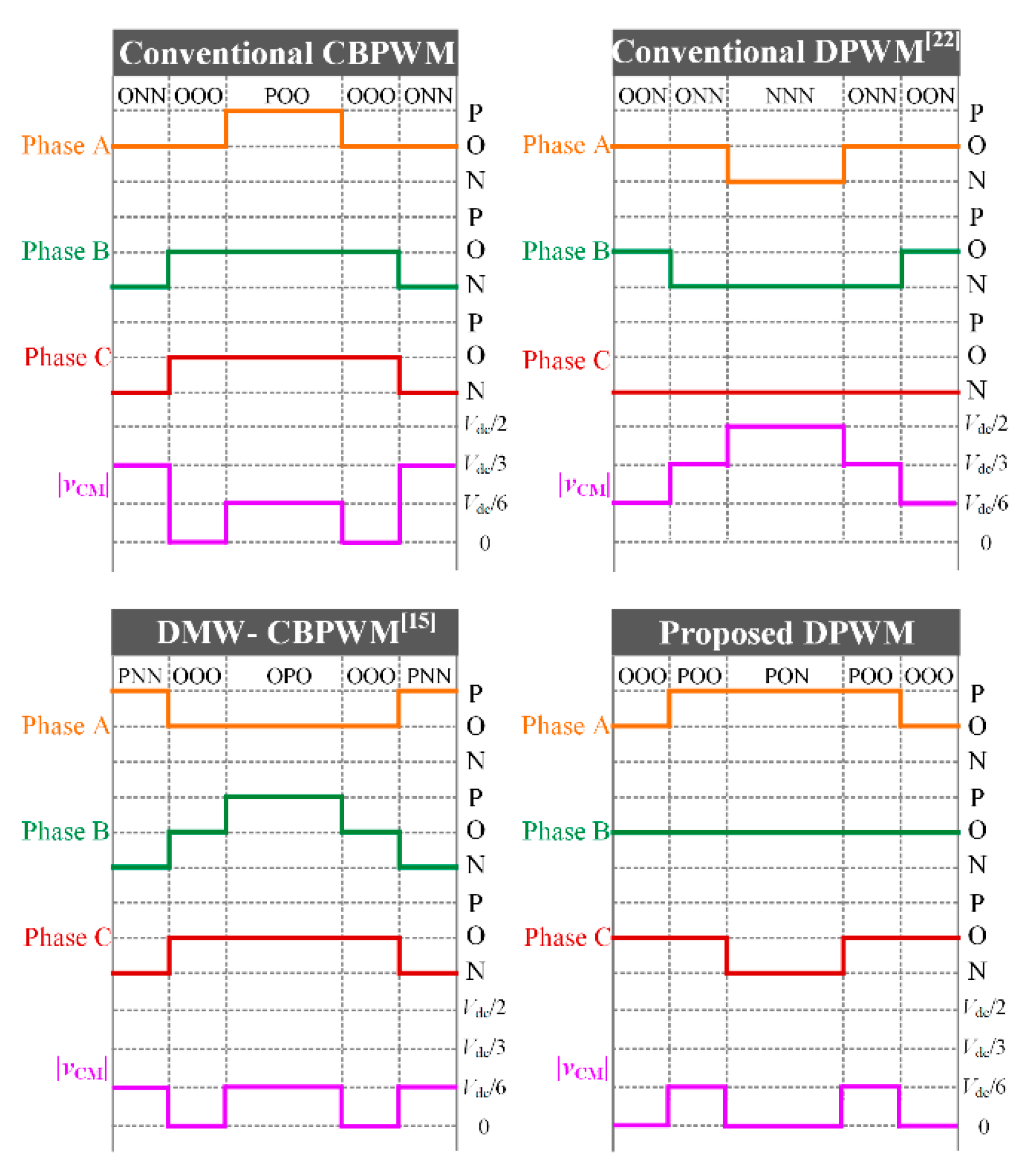
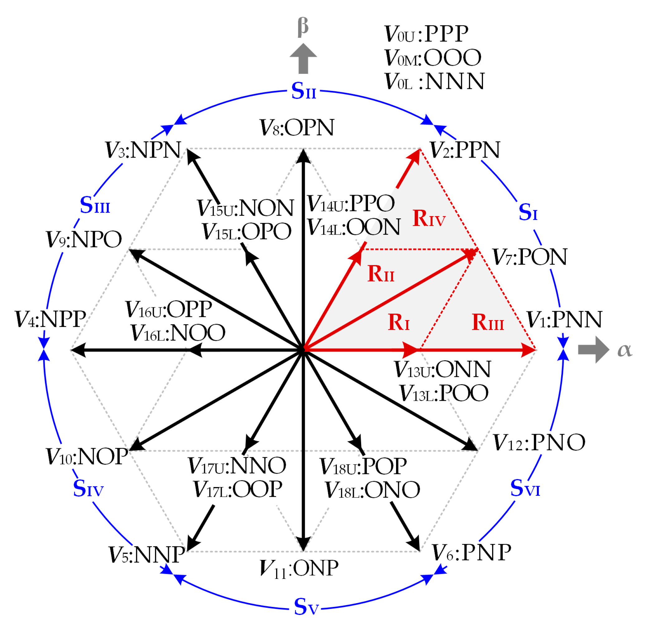
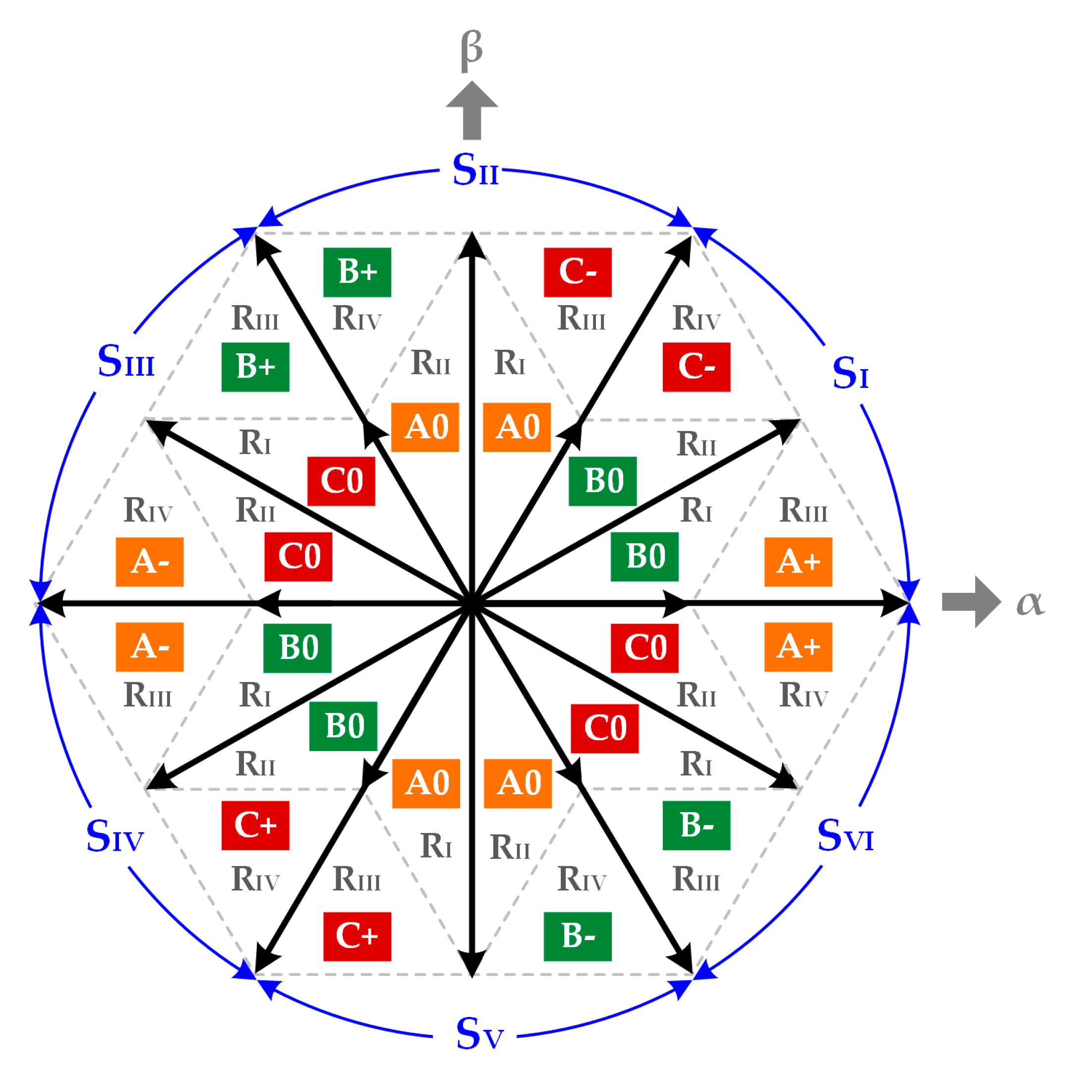
The space vector diagram can be divided into six sectors SI–SVI, with the large vector V1–V6 as the boundary. Each sector can be further divided into four regions RI–RIV. In order to reduce the CMV, small vectors V13U–V18U and zero vectors V0U and V0L are abandoned. While large vectors, medium vectors, small vectors V13L–V18L and zero vector V0M are adopted to synthesize the switching sequence. Thus, the amplitude of CMV can be limited to Vdc/6. Taking sector SI as an example:
In region RI, V0M: OOO, V7: PON and V13L: POO are used to synthesize the switching sequence;
In region RII, V0M: OOO, V7: PON and V14L: OON are used to synthesize the switching sequence;
In region RIII, V1: PNN, V7: PON and V13L: POO are used to synthesize the switching sequence;
In region RIV, V2: PPN, V7: PON and V14L: OON are used to synthesize the switching sequence.
From the aforementioned analysis, phase B is clamped to the switching state O in regions R
I and R
II. It can be defined as clamping state B0. Similarly, phase A is clamped to the switching state P in region R
III, and it can be defined as clamping state A+; phase C is clamped to the switching state N in region R
IV, and it can be defined as clamping state C−. The clamping state of other sectors can be obtained by replacing the vector in S
I by the corresponding vector that occupies the identical position in a given sector, as shown in
Figure 5.
4.2. Carrier-Based Implementation
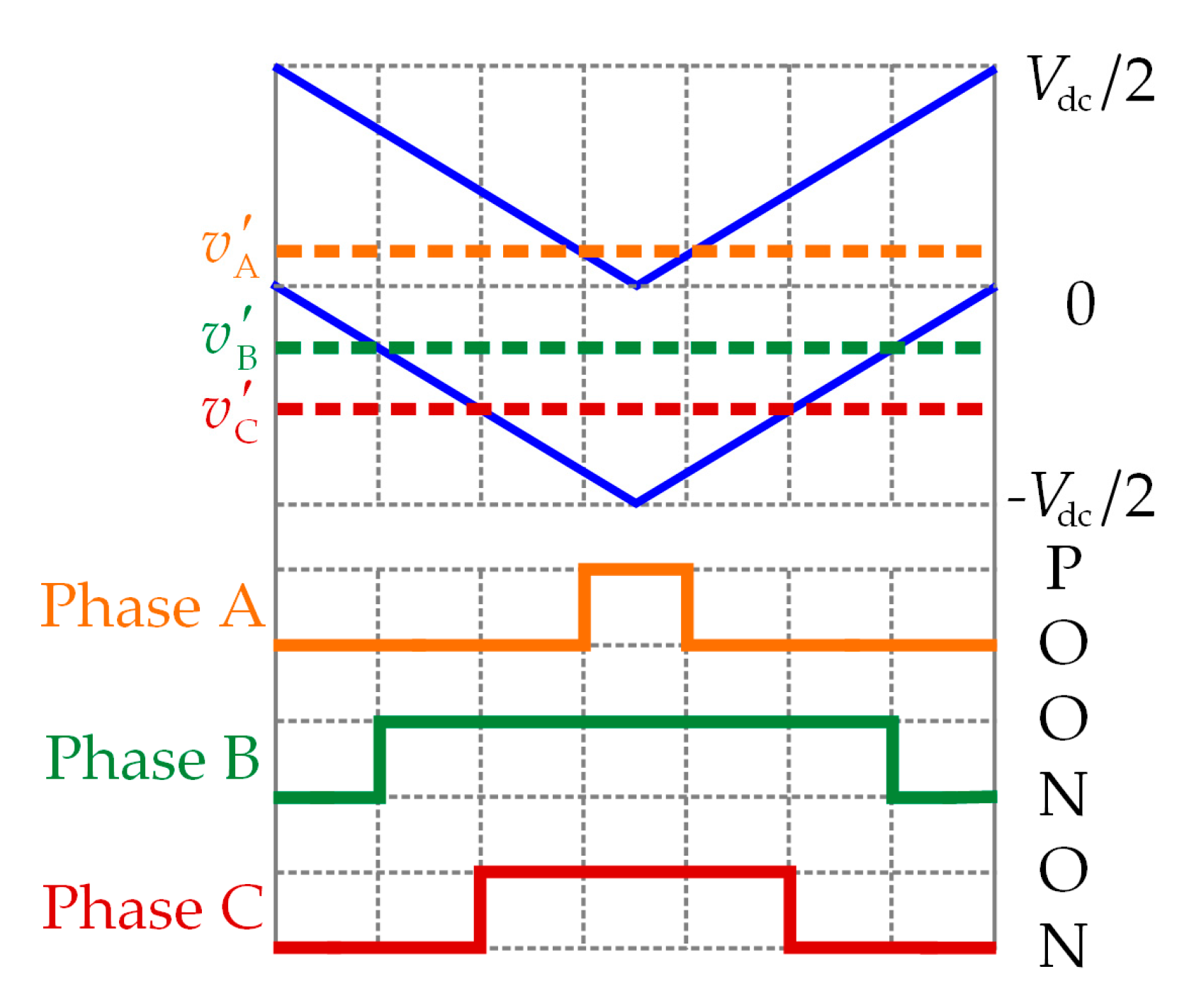
The aforementioned switching sequences can be obtained by the modification of both the reference voltage and the carrier. For the reference voltage, the specific zero-sequence voltage needs to be injected into the reference voltage to realize the clamping state in each region. The CMV and the switching loss are reduced simultaneously. For the carrier, the upper and lower carriers are changed from phase disposition to phase opposition disposition. The extra switches at the boundary of two adjacent regions are reduced. The detailed process is shown as follow:
Reference Vector Modification: The maximum, medium and minimum value of three-phase reference voltages
v′
x at any arbitrary instant can be obtained as follows:
where max (·), mid (·) and min (·) return the maximum, medium and minimum value of
v′
A,
v′
B and
v′
C. The relationship between
v′
max,
v′
mid,
v′
min and
vx in each sector is shown in
Table 3.
Taking sector SI as an example:
In region R
I and R
II, phase B needs to maintain clamping state 0. From
Table 3, the reference voltage of phase B is
v′
mid. Thus, −
v′
mid needs to be injected into
v′
B to keep the switching state of phase B at O.
In region RIII, phase A needs to maintain clamping state +. The reference voltage of phase A is v′max. Thus, −v′max + Vdc needs to be injected into v′A to keep the switching state of phase A at P.
In region RIV, phase C needs to maintain clamping state -. The reference voltage of phase C is v′min. Thus, −v′max − Vdc needs to be injected into v′C to keep the switching state of phase C at N.
In conclusion, in order to realize the clamping state in
Figure 5, zero-sequence voltage
vZ2 needs to be injected into the reference voltage
v′
x.
vZ2 can be expressed as:
The three-phase reference voltage after the injection of
vZ2 is
v″
x:
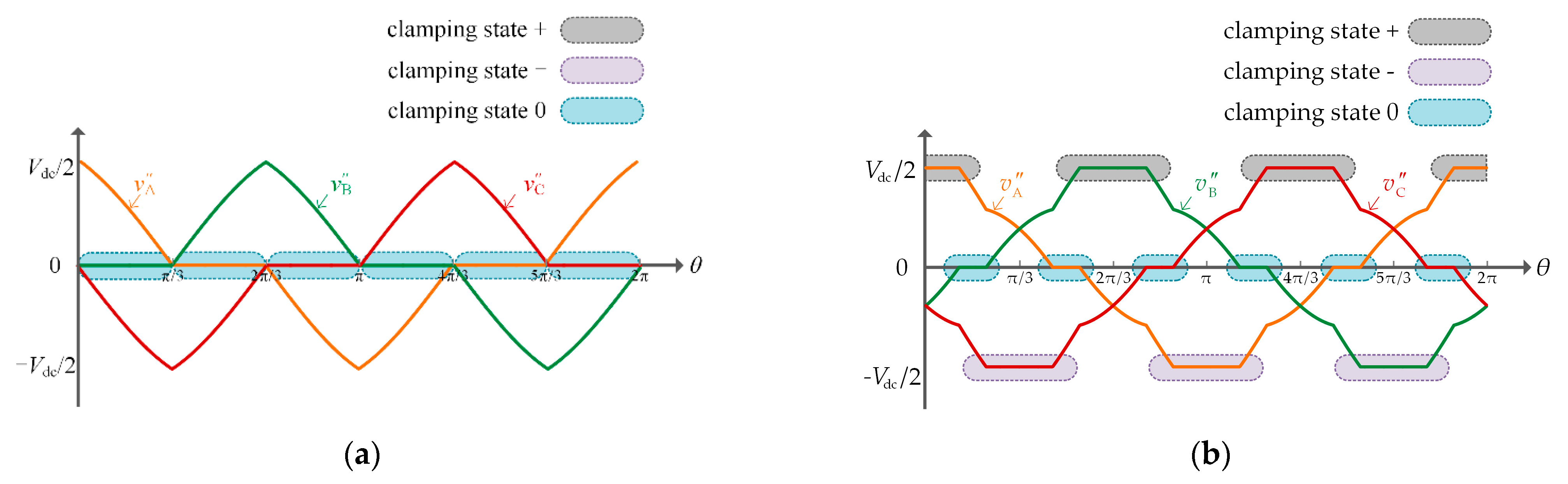
The three-phase reference voltages
v″
x in a unit fundamental period are shown in
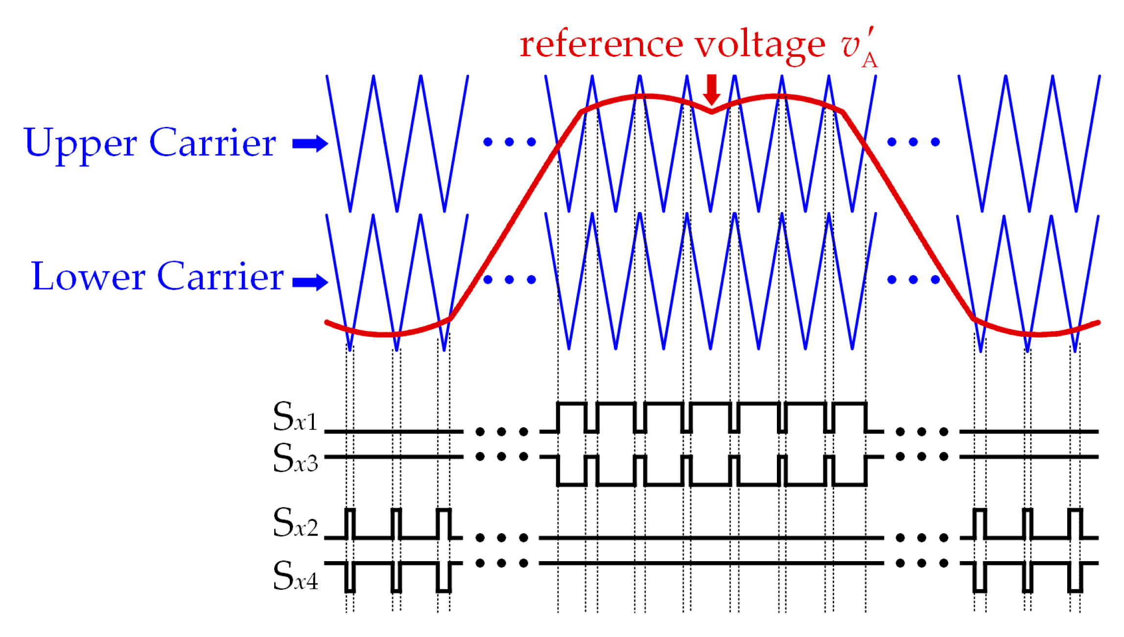
Figure 6. The switching states of the three phases are clamped to the positive bus, the negative bus and the neutral point of the DC-link alternatively, and the discontinuous modulation is realized.
Carrier Modification: For conventional CBPWM of the three-level inverter, the upper and lower-triangular carriers are in phase with each other. The PWM signals of each phase can be obtained by the comparison of the reference voltage
v″
x and two carriers. In sector S
I, when the reference voltage travels from region R
III to R
I, the reference voltage and the corresponding switching sequence are shown in
Figure 7a.
As can be seen, the switching sequence is PNN–PON–POO–PON–PNN in region R
III, and the amplitude of CMV is
Vdc/6. The switching sequence is OON–PON→POO–PON–OON in region R
I, and the amplitude of CMV is also
Vdc/6. Comparing
Figure 7a with
Figure 4, the amplitude of CMV is reduced from
Vdc/3 to
Vdc/6 by the injection of
vZ2. Moreover, the number of switches in each carrier period is reduced from 3 to 2. However, it is worth mentioning that there are extra switches during the transition of two adjacent regions. As shown in
Figure 7a, the last switching state of region R
III is PNN, and the first switching state of region R
I is OON. The switching states of phase A and phase B are both changed so that the switching loss is increased. To solve the above issue, the two triangle carriers need to be changed from phase disposition to phase opposition disposition, as shown in
Figure 7b. After that, the switching sequence in region R
III becomes POO–PON–PNN–PON–POO, and the switching sequence in region R
I becomes OOO–POO–PON–POO–OOO. The amplitude of CMV is still
Vdc/6. Meanwhile, only the switching state of phase A is changed during the transition of two adjacent regions.
In conclusion, the extra switches can be reduced by the phase opposition disposition of the carriers. Then the switching loss can be further suppressed.
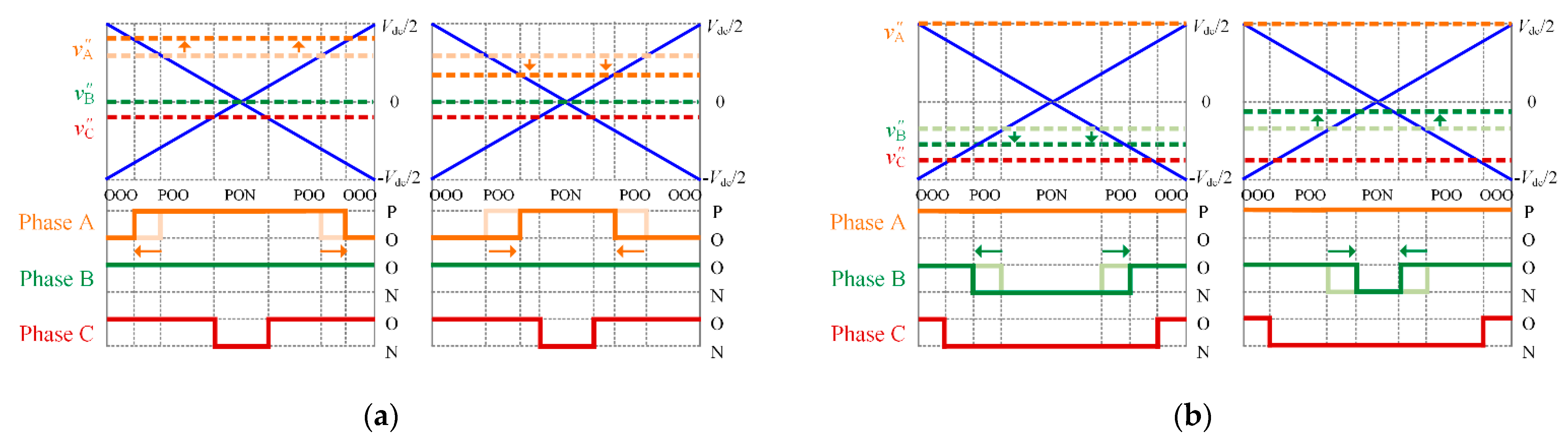
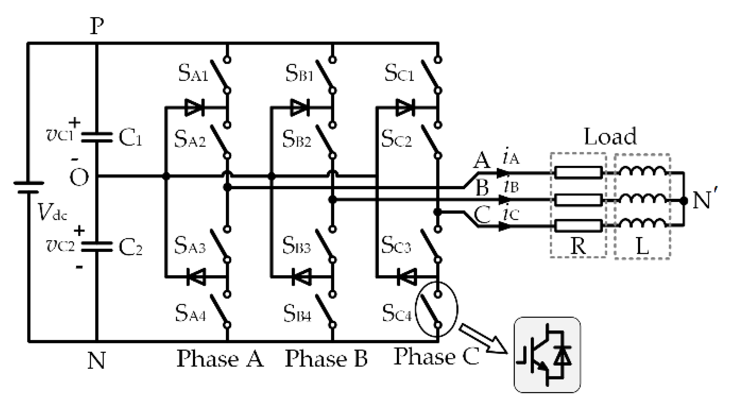
4.3. NPV Balance Control
In high-power medium-voltage applications, the NPV balance also needs to be considered, besides the CMV and the switching loss. The NPV is defined as Δv = vC1 − vC2, vth is the threshold value of Δv. When |Δv| < vth, the NPV does not need to be controlled. When |Δv| > vth, the NPV ripple must be suppressed. The voltages of the upper capacitor vC1 and lower capacitor vC2 are affected by the neutral point current iO. The neutral point currents are generated by small vectors and medium vectors. Thus, the NPV balance can be realized by adjusting the duty cycle of small and medium vectors in each region of different sectors.
Taking sector S
I as an example, the duty cycle of
V13L: POO (
iO = −
iA) can be adjusted to balance the NPV in region R
I. While the duty cycle of
V7: PON (
iO =
iB) can be adjusted to balance the NPV in region R
III. In region R
I, the neutral point current
iO generated by
V13L: POO is less than zero. When |Δ
v| > 0, the duty cycle of
V13L: POO needs to be increased. When |Δ
v| < 0, the duty cycle of
V13L: POO needs to be reduced. In region R
III, the neutral point current
iO generated by
V7: PON is greater than zero. When |Δ
v| > 0, the duty cycle of
V7: PON needs to be reduced. When |Δ
v| < 0, the duty cycle of
V13L: POO needs to be increased. Similarly, the duty cycle adjustment rules of small and medium vectors in other sectors are listed in
Table 4. The vectors in
Table 4 are defined as master vectors, and the other vectors in the same switching sequence are defined as slave vectors.
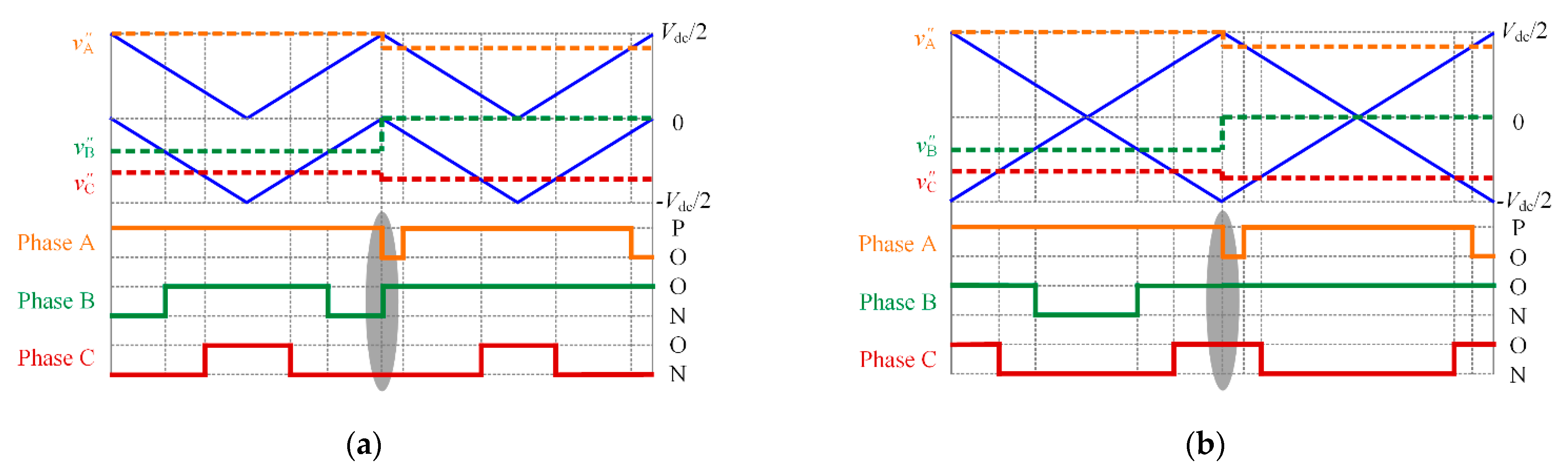
The duty cycle of the master vector can be adjusted by injecting the compensation voltage
vos into the reference voltage
v″
x to move the reference voltage up or down. Taking sector S
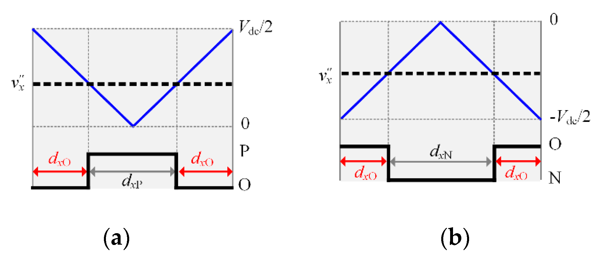
I as an example, in region R
I, the duty cycle of
V13L: POO will be increased if the reference voltage
v″
A is moved up. While the duty cycle of
V13L: POO will be reduced if the reference voltage
v″
A is moved down, as illustrated in
Figure 8a. In region R
III, the duty cycle of
V7: PON will be increased if the reference voltage
v″
B is moved down. While the duty cycle of
V7: PON will be reduced if the reference voltage
v″
B is moved up, as illustrated in
Figure 8b. It is worth mentioning that the shift of the reference voltage only changes the duty cycle of the master vector and vectors without affecting the NPV. Therefore, the NPV balance can be realized by the shift of the reference voltage.
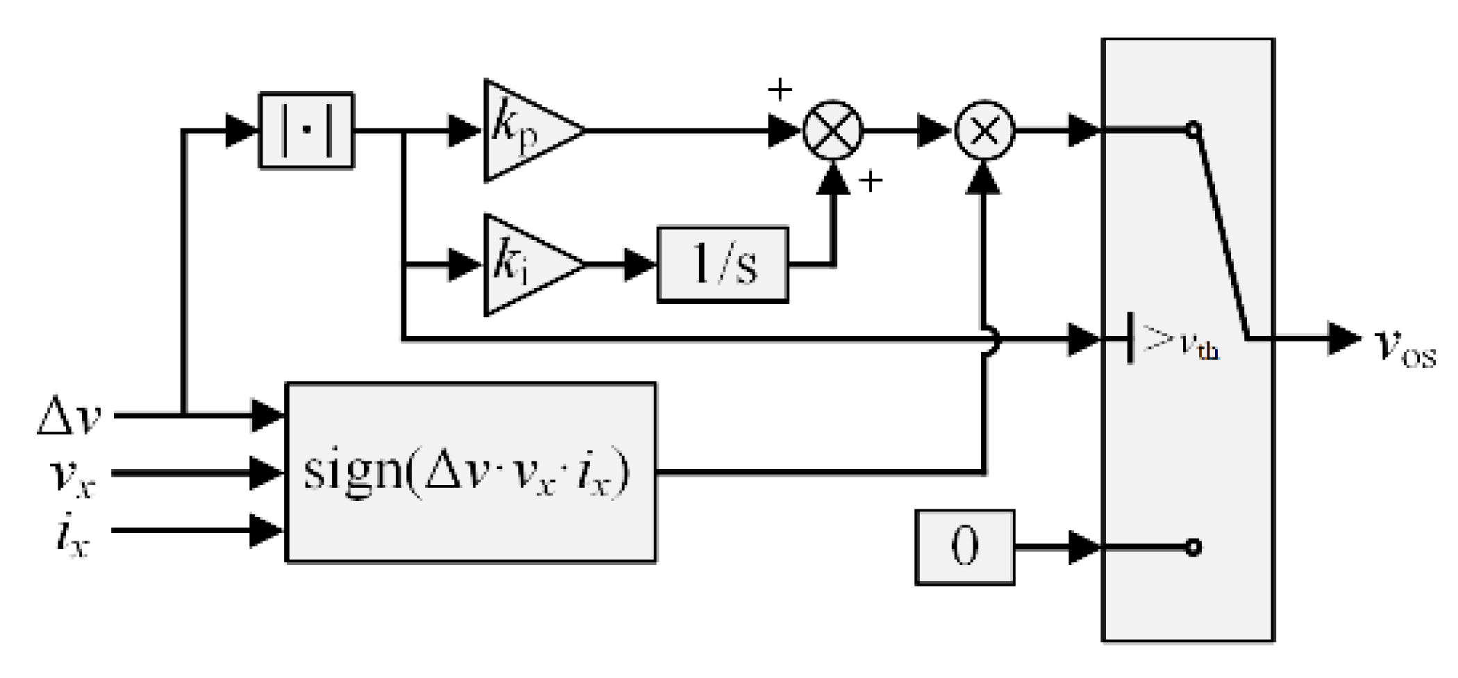
The calculation process of the compensation voltage
vos is shown in
Figure 9. When |Δ
v| <
vth,
vos is set to 0 and three-phase reference voltage
v″
x remains the same. When |Δ
v| >
vth, the compensation voltage
vos is obtained by multiplying the output of the PI controller by sign(Δ
v·
ix·
vx). Then,
vos is injected into
v″
x, according to
Table 5. The reference voltage
v*
x =
v″
x +
vos after the compensation.
For the NPV balance control, it is necessary to limit the amplitude of v*x to ensure that the switching sequence is not changed. When v″x > 0, v*x will be set to zero if v*x < 0, while v*x will be set to v″max if v*x > v″max. When v*x < 0, v*x will be set to zero if v*x > 0, while v*x will be set to v″min if v*x < v″min, where v″max and v″min are the maximum and minimum value of v″x.
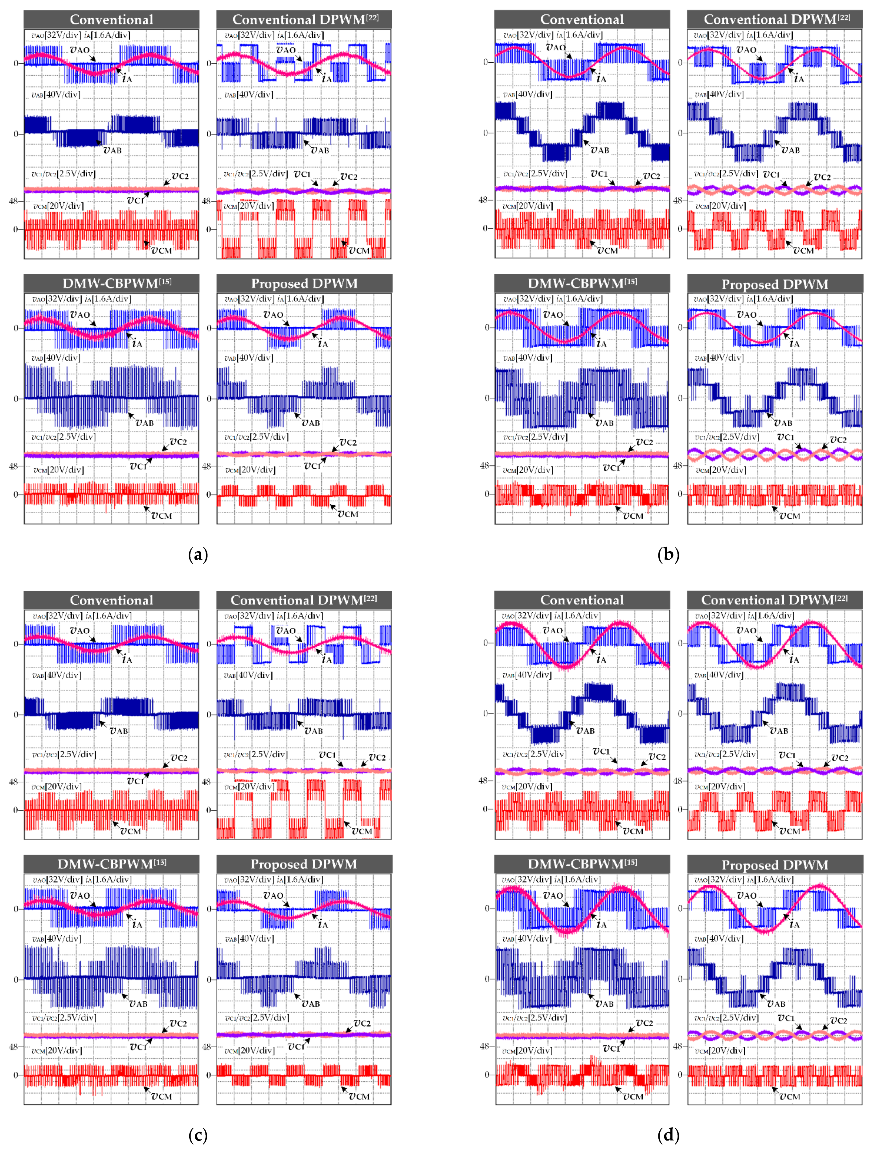
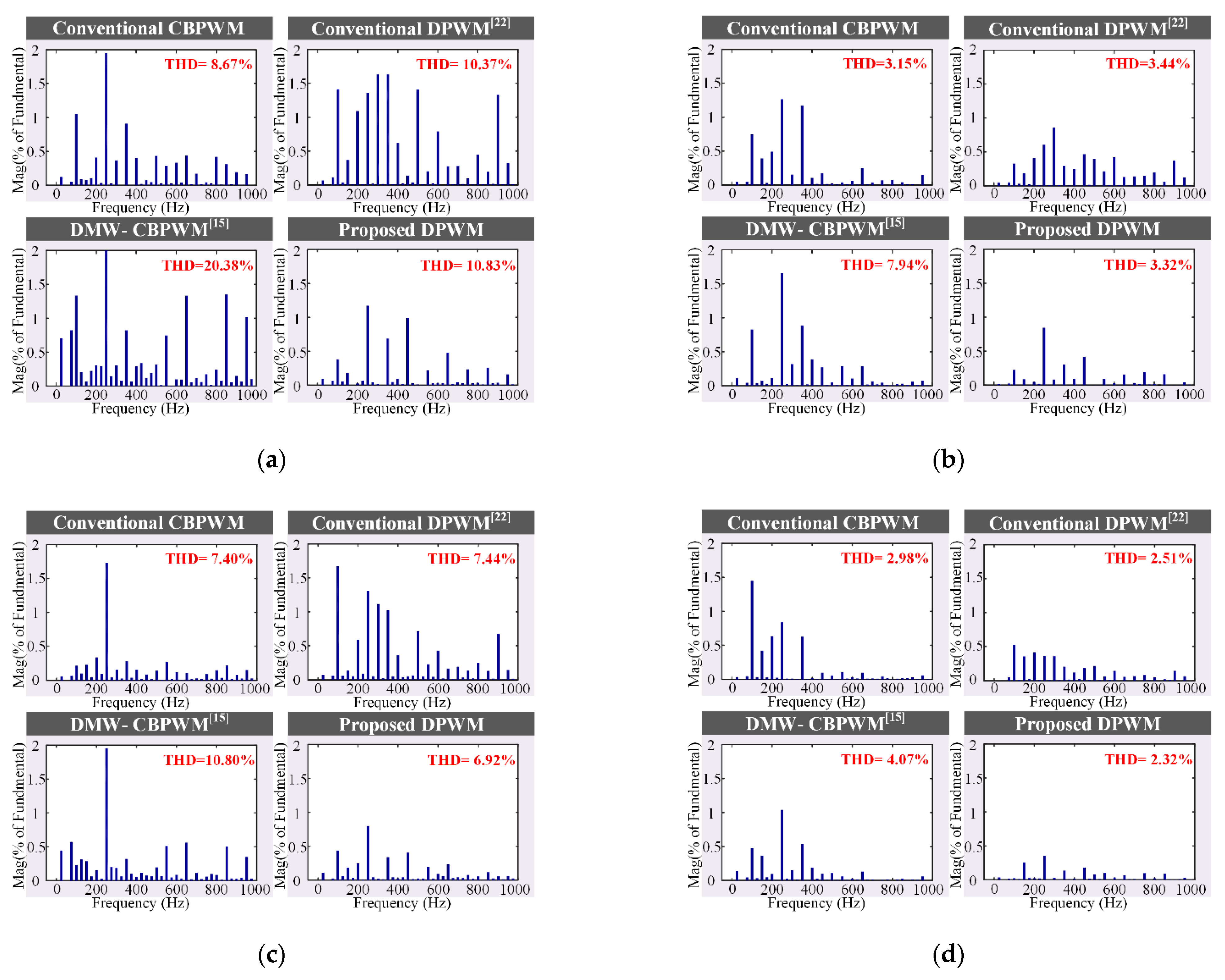
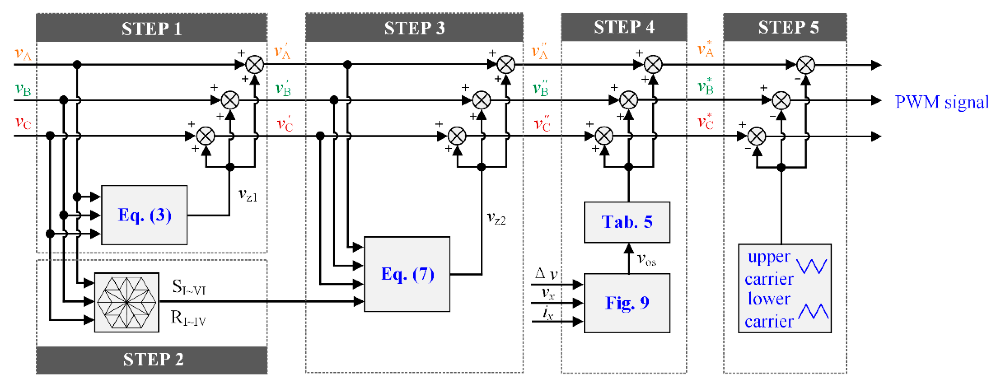
In conclusion, the CMV and the switching loss can be reduced by the modification of the reference voltage and the carriers. Meanwhile, the NPV balance can also be realized by the shift of the reference voltage without changing the switching sequence. The block diagram of the proposed DPWM is shown in
Figure 10. The detailed steps are listed as follows:
STEP 1: the zero-sequence voltage vZ1 is injected into the reference voltage vx;
STEP 2: the sector and region are determined by the three-phase reference voltage;
STEP 3: the zero-sequence voltage vZ2 is injected into the reference voltage v′x;
STEP 4: the compensation voltage vos is generated and injected into the reference voltage v″x;
STEP 5: the pulse signal of each power switch is generated by the comparison of the reference voltage v*x and the carriers.


