Abstract
For the conventional carrier-based pulse width modulation (CBPWM) strategies of neutral point clamped (NPC) three-level inverters, the higher common-mode voltage (CMV) is a major drawback. However, with CMV suppression strategies, the switching loss is relatively high. In order to solve the above issue, a carrier-based discontinuous PWM (DPWM) strategy for NPC three-level inverter is proposed in this paper. Firstly, the reference voltage is modified by the twice injection of zero-sequence voltage. Switching states of the three-phase are clamped alternatively to reduce both the CMV and the switching loss. Secondly, the carriers are also modified by the phase opposite disposition of the upper and lower carriers. The extra switching at the border of two adjacent regions in the space vector diagram is reduced. Meanwhile, a neutral-point voltage (NPV) control method is also presented. The duty cycle of the switching state that affects the NPV is adjusted to obtain the balance control of the NPV. Still, the switching sequence in each carrier period remains the same. Finally, the feasibility and effectiveness of the proposed DPWM strategy are tested on a rapid control prototype platform based on RT-Lab.
1. Introduction
Compared with two-level inverters, NPC three-level inverters have advantages of lower output harmonics distortion and lower dv/dt of the power device. Thus, it is widely used in medium-voltage high-power traction applications, such as locomotive traction and ship propulsion [1,2,3].
The common-mode voltage emerges between neutral points of DC-link capacitors and stator windings in NPC three-level inverter fed motor system. Numerous hazards are associated with the common-mode voltage. First, the shaft voltage is brought out on the motor bearing, and the life of the motor will be shortened by the shaft current [4]. Secondly, there are high-frequency components in the common-mode voltage. They would cause electromagnetic interference to the power supply [5]. Thirdly, the insulation stress of stator windings is also increased by the CMV. Thus, the aging process of the motor is accelerated [6]. These problems will get worse if the inverter is applied to the medium-voltage high-power traction application.
For three-level inverters, there are two ways commonly used to reduce the CMV. The first is the improvement of topology, and the second is the improvement of modulation strategy. For the former, the CMV can be reduced by several methods, such as the addition of the fourth bridge [7,8], the modification of the DC-link structure [9], the addition of the common-mode inductance [10] and the addition of the filter [11,12]. All the above methods impose extra hardware on the system, resulting in an increase in cost, volume and loss. For the latter, there is no need for any additional hardware so that it attracts more attention all over the world.
The common feature of CMV suppression PWM strategies is that switching states with the lower CMV are adopted to synthesize the switching sequence. In [13], five switching states with the lowest CMV are used to synthesize the switching sequence in each carrier period. Although the CMV can be reduced effectively, the switching loss is inevitably increased. In [14], only the switching state with zero amplitude of CMV can be used, and the output harmonic distortion of the inverter is improved by the proper arrangement of these switching states in each carrier period. However, there are seven switching states in each switching sequence, and the inverter suffers from lower DC-link voltage utilization and higher switching loss. A double modulation wave carrier-based PWM strategy (DMW-CBPWM) is proposed in [15], the reference voltage is modified to reduce the CMV and the NPV ripple simultaneously. In [16,17], four switching states with lower CMV are used to synthesize the switching sequence in each carrier period, and the NPV balance control is achieved by adjusting the duty cycle of the switching states. In [18], carriers are phase opposition arranged, the CMV and the NPV ripple are both suppressed by injecting the DC component into the reference voltage.
With the promotion of power and voltage levels, the switching loss becomes the main component of the overall loss of the system [19,20,21]. Thus, the CMV and the switching loss should be both taken into consideration. Conventional CMV suppression PWM strategies only focus on the performance of CMV and are not suitable for medium-voltage high-power traction applications. DPWM methods are well known to reduce the switching loss and harmonic distortion at a given average switching frequency. Thus, DPWM strategies are extremely suitable for high-power medium-voltage three-level inverters. The conventional DPWMs for a three-level inverter are proposed in [22]. In [23], an improved DPWM is presented to reduce the switching loss and the harmonic distortion. However, the CMV is still larger under higher modulation index conditions.
For the purpose of suppressing CMV and switching loss simultaneously, a carrier-based DPWM strategy is proposed in this paper. By the modification of the reference voltage, switching states with higher CMV are eliminated in the synthesis of the switching sequence. One of the three phases is clamped to a certain switching state in each switching sequence. Thus, the CMV and the switching loss are both reduced. By the modification of the carriers, the extra switches during the transient process of two adjacent regions are decreased to further reduce the switching loss. The proposed DPWM strategy is validated through experimental results. The experimental setup comprises an OPAL-RT OP5700 rapid control prototype and an NPC three-level inverter fed R-L load.
2. NPC Three-Level Inverter and CBPWM
2.1. Topology of the NPC Three-Level Inverter
The topology of the NPC three-level inverter is shown in Figure 1. The DC-link voltage Vdc is equally divided into the upper-capacitor voltage vC1 and the lower-capacitor voltage vC2. iA, iB and iC are the three-phase load currents, respectively.
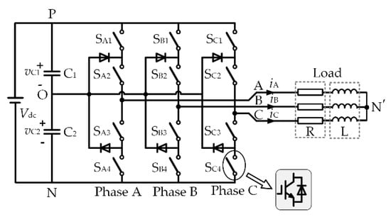
Figure 1.
The topology of the NPC three-level inverter.
The switching states of the three-level inverter are defined in Table 1.

Table 1.
The definition of switching state for NPC three-level inverter.
The space vector diagram for the three-level inverter is shown in Figure 2, with 33 = 27 basic vectors. According to the amplitude, the basic vectors can be divided into four categories: large vector V1–V6, medium vector V7–V12, small vector V13U–V18U, V13L–V18L and zero vector V0U, V0M, V0L. As can be seen, there are two small vectors that occupy the same position, and they are defined as redundant vectors. The definition is also suitable for zero vectors.
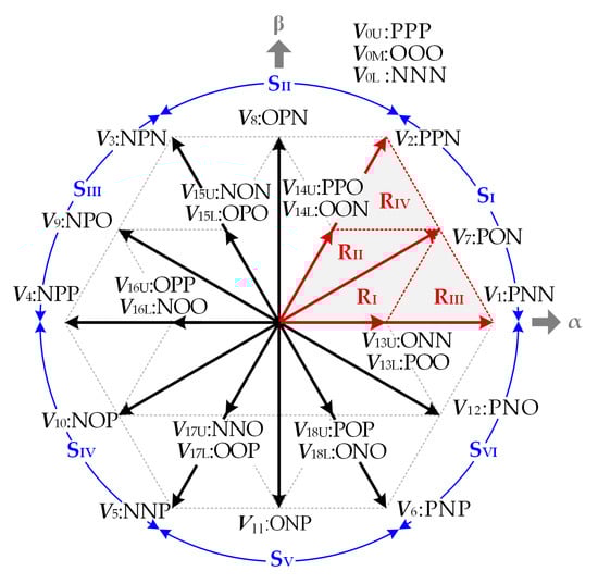
Figure 2.
The space vector diagram of the NPC three-level inverter.
2.2. CBPWM of the Three-Level Inverter
For conventional CBPWM of the three-level inverter, the pulse signal for each power device is produced by the comparison of the carriers and the reference voltage vx, (x ∈ {A, B, C}). The reference voltages of the three phases are defined as:
where θ is the phase angle of the reference voltage and m is the modulation index. The modulation index is defined as:
where Vm is the amplitude of the reference voltage within the linear modulation range, m ∈ [0, 1]. For sinusoidal PWM (SPWM), the DC-link voltage is not fully utilized compared with space vector PWM (SVPWM). This problem can be solved by the injection of the zero-sequence voltage vZ1:
where vmax = max (vA, vB, vC) and vmin = min (vA, vB, vC) are the maximum and minimum values of the three-phase reference voltage at any arbitrary instant. After the injection of vZ1, the reference voltage is modified to:
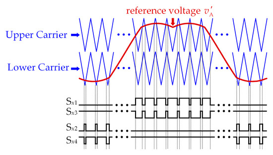
Figure 3.
The reference voltage and the carriers of the conventional CBPWM.
The switching sequence of each phase can be obtained by the comparison of the reference voltage and the two-phase disposition carriers. The switching sequence of a unit carrier period is shown in Figure 4.
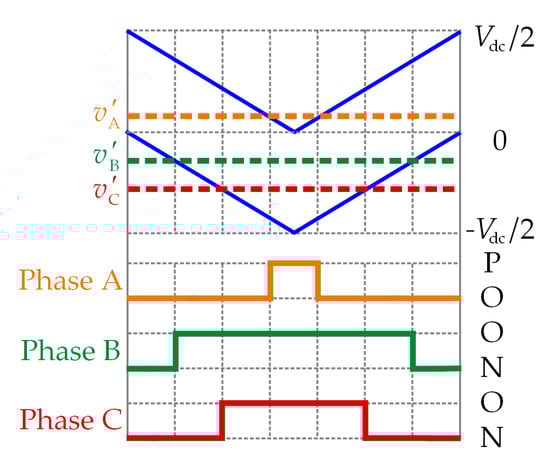
Figure 4.
The switching sequence in a unit carrier period.
3. Analysis of CMV and Switching Frequency of the Three-Level Inverter
3.1. Common-Mode Voltage
The CMV of a three-level inverter refers to the voltage between the neutral point of the DC-link capacitors and the neutral point of the three-phase loads, which is defined as:
where vCM is the common-mode voltage. vAO, vBO and vCO are the three-phase voltages, respectively. From (5) and Table 1, the CMV of each basic vector can be obtained, as shown in Table 2.
Table 2.
Common-mode voltage of each basic vector.
The amplitude of CMV for a certain switching sequence is determined by the basic vector with the largest amplitude of CMV. Taking switching sequence V13U–V14L–V0M–V13L (ONN–OON–OOO–POO) as an example (as shown in Figure 4), the amplitude of CMV is Vdc/3. Obviously, the small and zero vectors with the lower amplitude of CMV need to be adopted during the synthesis of the switching sequence in order to reduce the amplitude of CMV.
3.2. Switching Frequency
As shown in Figure 4, small vectors V13U and V13L are both used to synthesize the switching sequence. The switching state of these phases is all changed so that the switching sequence belongs to continuous PWM (CPWM). If only the small vector V13U is adopted, the switching sequence will become V13U–V14L–V0M (ONN–OON–OOO). While if only the small vector V13L is adopted, the switching sequence will become V14L–V0M–V13L (OON–OOO–POO). For the above two sequences, the switching states of phase A and C are both changed, but the switching state of phase B remains the same. Thus, these switching sequences belong to DPWM. By the use of DPWM, Only one of the redundant vectors appears in each carrier period. As a result, the switching loss can be reduced.
4. Proposed Carrier-Based Discontinuous PWM Strategy
4.1. Switching Sequence Design
The space vector diagram can be divided into six sectors SI–SVI, with the large vector V1–V6 as the boundary. Each sector can be further divided into four regions RI–RIV. In order to reduce the CMV, small vectors V13U–V18U and zero vectors V0U and V0L are abandoned. While large vectors, medium vectors, small vectors V13L–V18L and zero vector V0M are adopted to synthesize the switching sequence. Thus, the amplitude of CMV can be limited to Vdc/6. Taking sector SI as an example:
- In region RI, V0M: OOO, V7: PON and V13L: POO are used to synthesize the switching sequence;
- In region RII, V0M: OOO, V7: PON and V14L: OON are used to synthesize the switching sequence;
- In region RIII, V1: PNN, V7: PON and V13L: POO are used to synthesize the switching sequence;
- In region RIV, V2: PPN, V7: PON and V14L: OON are used to synthesize the switching sequence.
From the aforementioned analysis, phase B is clamped to the switching state O in regions RI and RII. It can be defined as clamping state B0. Similarly, phase A is clamped to the switching state P in region RIII, and it can be defined as clamping state A+; phase C is clamped to the switching state N in region RIV, and it can be defined as clamping state C−. The clamping state of other sectors can be obtained by replacing the vector in SI by the corresponding vector that occupies the identical position in a given sector, as shown in Figure 5.
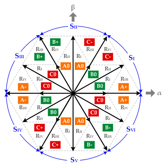
Figure 5.
The clamping state in each region of the space vector diagram.
4.2. Carrier-Based Implementation
The aforementioned switching sequences can be obtained by the modification of both the reference voltage and the carrier. For the reference voltage, the specific zero-sequence voltage needs to be injected into the reference voltage to realize the clamping state in each region. The CMV and the switching loss are reduced simultaneously. For the carrier, the upper and lower carriers are changed from phase disposition to phase opposition disposition. The extra switches at the boundary of two adjacent regions are reduced. The detailed process is shown as follow:
Reference Vector Modification: The maximum, medium and minimum value of three-phase reference voltages v′x at any arbitrary instant can be obtained as follows:
where max (·), mid (·) and min (·) return the maximum, medium and minimum value of v′A, v′B and v′C. The relationship between v′max, v′mid, v′min and vx in each sector is shown in Table 3.
Table 3.
Relationship between v′max, v′mid, v′min and v′x.
Taking sector SI as an example:
In region RI and RII, phase B needs to maintain clamping state 0. From Table 3, the reference voltage of phase B is v′mid. Thus, −v′mid needs to be injected into v′B to keep the switching state of phase B at O.
In region RIII, phase A needs to maintain clamping state +. The reference voltage of phase A is v′max. Thus, −v′max + Vdc needs to be injected into v′A to keep the switching state of phase A at P.
In region RIV, phase C needs to maintain clamping state -. The reference voltage of phase C is v′min. Thus, −v′max − Vdc needs to be injected into v′C to keep the switching state of phase C at N.
In conclusion, in order to realize the clamping state in Figure 5, zero-sequence voltage vZ2 needs to be injected into the reference voltage v′x. vZ2 can be expressed as:
The three-phase reference voltage after the injection of vZ2 is v″x:
The three-phase reference voltages v″x in a unit fundamental period are shown in Figure 6. The switching states of the three phases are clamped to the positive bus, the negative bus and the neutral point of the DC-link alternatively, and the discontinuous modulation is realized.
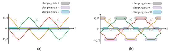
Figure 6.
The reference voltage after the second injection of the zero-sequence voltage. (a) m = 0.3; (b) m = 0.8.
Carrier Modification: For conventional CBPWM of the three-level inverter, the upper and lower-triangular carriers are in phase with each other. The PWM signals of each phase can be obtained by the comparison of the reference voltage v″x and two carriers. In sector SI, when the reference voltage travels from region RIII to RI, the reference voltage and the corresponding switching sequence are shown in Figure 7a.
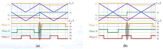
Figure 7.
The switching sequence of the transition from region RIII to RI. (a) Phase disposition condition; (b) Phase opposition disposition condition.
As can be seen, the switching sequence is PNN–PON–POO–PON–PNN in region RIII, and the amplitude of CMV is Vdc/6. The switching sequence is OON–PON→POO–PON–OON in region RI, and the amplitude of CMV is also Vdc/6. Comparing Figure 7a with Figure 4, the amplitude of CMV is reduced from Vdc/3 to Vdc/6 by the injection of vZ2. Moreover, the number of switches in each carrier period is reduced from 3 to 2. However, it is worth mentioning that there are extra switches during the transition of two adjacent regions. As shown in Figure 7a, the last switching state of region RIII is PNN, and the first switching state of region RI is OON. The switching states of phase A and phase B are both changed so that the switching loss is increased. To solve the above issue, the two triangle carriers need to be changed from phase disposition to phase opposition disposition, as shown in Figure 7b. After that, the switching sequence in region RIII becomes POO–PON–PNN–PON–POO, and the switching sequence in region RI becomes OOO–POO–PON–POO–OOO. The amplitude of CMV is still Vdc/6. Meanwhile, only the switching state of phase A is changed during the transition of two adjacent regions.
In conclusion, the extra switches can be reduced by the phase opposition disposition of the carriers. Then the switching loss can be further suppressed.
4.3. NPV Balance Control
In high-power medium-voltage applications, the NPV balance also needs to be considered, besides the CMV and the switching loss. The NPV is defined as Δv = vC1 − vC2, vth is the threshold value of Δv. When |Δv| < vth, the NPV does not need to be controlled. When |Δv| > vth, the NPV ripple must be suppressed. The voltages of the upper capacitor vC1 and lower capacitor vC2 are affected by the neutral point current iO. The neutral point currents are generated by small vectors and medium vectors. Thus, the NPV balance can be realized by adjusting the duty cycle of small and medium vectors in each region of different sectors.
Taking sector SI as an example, the duty cycle of V13L: POO (iO = −iA) can be adjusted to balance the NPV in region RI. While the duty cycle of V7: PON (iO = iB) can be adjusted to balance the NPV in region RIII. In region RI, the neutral point current iO generated by V13L: POO is less than zero. When |Δv| > 0, the duty cycle of V13L: POO needs to be increased. When |Δv| < 0, the duty cycle of V13L: POO needs to be reduced. In region RIII, the neutral point current iO generated by V7: PON is greater than zero. When |Δv| > 0, the duty cycle of V7: PON needs to be reduced. When |Δv| < 0, the duty cycle of V13L: POO needs to be increased. Similarly, the duty cycle adjustment rules of small and medium vectors in other sectors are listed in Table 4. The vectors in Table 4 are defined as master vectors, and the other vectors in the same switching sequence are defined as slave vectors.
Table 4.
Master vector in each region.
The duty cycle of the master vector can be adjusted by injecting the compensation voltage vos into the reference voltage v″x to move the reference voltage up or down. Taking sector SI as an example, in region RI, the duty cycle of V13L: POO will be increased if the reference voltage v″A is moved up. While the duty cycle of V13L: POO will be reduced if the reference voltage v″A is moved down, as illustrated in Figure 8a. In region RIII, the duty cycle of V7: PON will be increased if the reference voltage v″B is moved down. While the duty cycle of V7: PON will be reduced if the reference voltage v″B is moved up, as illustrated in Figure 8b. It is worth mentioning that the shift of the reference voltage only changes the duty cycle of the master vector and vectors without affecting the NPV. Therefore, the NPV balance can be realized by the shift of the reference voltage.
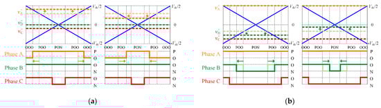
Figure 8.
The influence of vos on the switching sequence. (a) Adjustment of V13L in region RIII; (b) Adjustment of V7 in region RI.
The calculation process of the compensation voltage vos is shown in Figure 9. When |Δv| < vth, vos is set to 0 and three-phase reference voltage v″x remains the same. When |Δv| > vth, the compensation voltage vos is obtained by multiplying the output of the PI controller by sign(Δv·ix·vx). Then, vos is injected into v″x, according to Table 5. The reference voltage v*x = v″x + vos after the compensation.
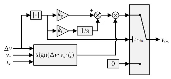
Figure 9.
The calculation process of vos.
Table 5.
Compensation voltage injection rules.
For the NPV balance control, it is necessary to limit the amplitude of v*x to ensure that the switching sequence is not changed. When v″x > 0, v*x will be set to zero if v*x < 0, while v*x will be set to v″max if v*x > v″max. When v*x < 0, v*x will be set to zero if v*x > 0, while v*x will be set to v″min if v*x < v″min, where v″max and v″min are the maximum and minimum value of v″x.
In conclusion, the CMV and the switching loss can be reduced by the modification of the reference voltage and the carriers. Meanwhile, the NPV balance can also be realized by the shift of the reference voltage without changing the switching sequence. The block diagram of the proposed DPWM is shown in Figure 10. The detailed steps are listed as follows:
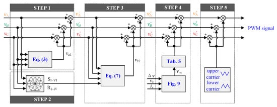
Figure 10.
Block diagram of the proposed DPWM strategy.
- STEP 1: the zero-sequence voltage vZ1 is injected into the reference voltage vx;
- STEP 2: the sector and region are determined by the three-phase reference voltage;
- STEP 3: the zero-sequence voltage vZ2 is injected into the reference voltage v′x;
- STEP 4: the compensation voltage vos is generated and injected into the reference voltage v″x;
- STEP 5: the pulse signal of each power switch is generated by the comparison of the reference voltage v*x and the carriers.
5. Experimental Verification
In order to verify the feasibility and effectiveness of the proposed DPWM strategy, the rapid control prototype OP5700 (OPAL-RT Co. Ltd.,Richardson, Canada) and the NPC three-level power model PEN8018 (Imperix Co. Ltd., Sion, Switzerland) are adopted to establish the experimental setup, as shown in Figure 11.
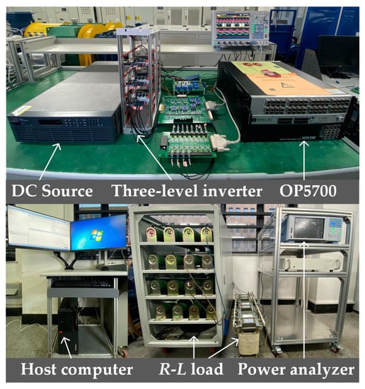
Figure 11.
The prototype of OPAL-RT® OP5700 driven three-level inverter.
The proposed DPWM strategy is compared with the conventional CBPWM, the conventional DPWM [22] and the DMW-CBPWM [15]. Parameters of the experimental setup are listed in Table 6. When R = 10 Ω and L = 10 mH, the power factor cos φ is 0.954. When R = 10 Ω and L = 30 mH, the power factor cos φ is 0.732.
Table 6.
Experimental parameters of the prototype.
The phase voltage vAO, line voltage vAB, phase current iA, common-mode voltage vCM and the upper and lower-capacitor voltages vC1/vC2 are shown in Figure 12.
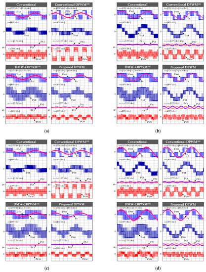
Figure 12.
Experimental results of phase voltage vAO, current iA, line voltage vAB, upper and lower-capacitor voltages vC1/vC2 and common voltage vCM. (a) m = 0.3, cos θ = 0.954; (b) m = 0.8, cos θ = 0.954; (c) m = 0.3, cos θ = 0.732; (d) m = 0.3, cos θ = 0.732.
5.1. Common-Mode Voltage
The switching sequences and the corresponding CMV of the four tested strategies in a unit carrier period are shown in Figure 13. For the conventional CBPWM, small vectors ViU (i ∈ {13, 14, …, 18}) are used to synthesize the switching sequence. For the conventional DPWM, zero vector V0U and V0L are used to synthesize the switching sequence. Thus, the amplitude of the CMV is higher for these two strategies. For the DMW-CBPWM and the proposed DPWM, small vector ViU, zero vector V0U and V0L are abandoned so that the amplitude of the CMV is lower. As can be seen in Figure 12, the amplitude of the CMV is 33.33 V (Vdc/3) for the conventional CBPWM. The amplitude of CMV is 50 V (Vdc/2) for the conventional DPWM. The amplitude of the CMV is 16.67 V (Vdc/6) for the DMW-CBPWM and the proposed DPWM.
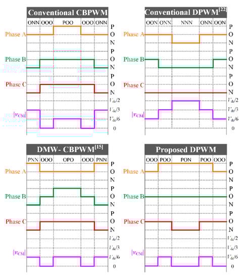
Figure 13.
Switching sequences and the corresponding CMV in a unit carrier period for the four tested strategies.
5.2. Switching Loss
In each carrier period, the switch time of the conventional DPWM and the proposed DPWM strategy is two, the switch time of the conventional CBPWM is three and the switch time of the DMW-CBPWM is four, as shown in Figure 13. The efficiency of the inverter with the above four strategies is recorded by Yokogawa WT5000 power analyzer, as listed in Table 7. The efficiency of the proposed DPWM is higher than the other three strategies, which verifies that the switching loss of the inverter can be suppressed by the proposed DPWM.
Table 7.
The efficiency of the inverter under different strategies.
5.3. Harmonic Distortion
As shown in Figure 12, the output current ripple of DMW-CBPWM is the highest. The output current ripple of the other three strategies is not very different from each other. By the FFT analysis of the experimental results, the harmonics spectra of the output current waveforms under m = 0.3 and m = 0.8 are shown in Figure 14. Under lower modulation index and higher power factor conditions, the THD of the proposed DPWM is greater than Conventional CBPWM and Conventional DPWM but less than DMW-CBPWM. Under lower power factor conditions, regardless of the modulation index, the THD of the proposed DPWM is smaller than the other three strategies. Therefore, the output waveform quality of the inverter can be improved by the proposed DPWM strategy under certain load conditions.
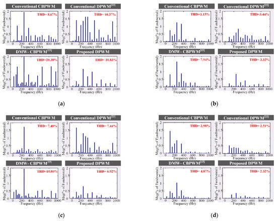
Figure 14.
Harmonic spectra of iA under different modulation index conditions. (a) m = 0.3, cos θ = 0.954; (b) m = 0.8, cos θ = 0.954; (c) m = 0.3, cos θ = 0.732; (d) m = 0.3, cos θ = 0.732.
5.4. Neutral Point Voltage
If |Δv| < vth, the NPV will not be controlled. As shown in Figure 12, the upper and lower-capacitor voltages are approximately the same for all four strategies under lower-modulation index conditions. Under higher-modulation index conditions, there are low-frequency components, which are 150 Hz (three times the fundamental frequency of output current), in both the upper and lower-capacitor voltages for the conventional CBPWM, the conventional DPWM and the proposed DPWM. However, the neutral point voltage is still self-balanced on the fundamental period level. Taking the proposed DPWM as an example, the detailed analysis is as follows. After the injection of vZ2, the dwell time of switching state O for each phase can be expressed as:
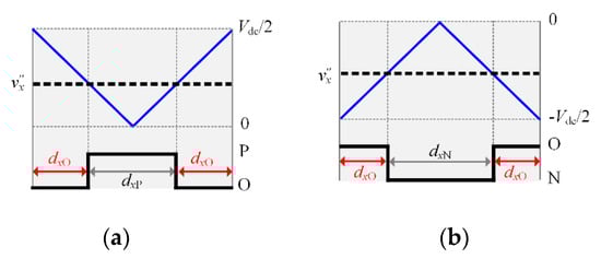
Figure 15.
Duty cycles of switching state O of a certain phase in a unit carrier period. (a) condition of v″x > 0; (b) condition of v″x < 0.
The reference voltage, output current and the neutral point current can be regarded as the function of the phase angle θ. Taking sector SI as an example, when the reference voltage is in region RI, phase B is clamped to switching state O and dBO = 1. Substituting (7), (8) and (9) into (10), yields:
When the phase angle is θ + π/3, phase A is clamped to the switching state O and dAO = 1. The neutral point current is:
The reference voltage and the output current are three-phase symmetrized.
Substituting (13) into (12), yields that iO(θ) = −iO(θ + π/3). It indicates that the NPV generated by the neutral point current at any arbitrary instant will be offset by the neutral point current lagging π/3. Thus, there is always a triple fundamental frequency component in the neutral point voltage. However, the neutral point can still be considered balanced on a fundamental period level; as shown in Figure 12a,b.
If |Δv| > vth, the proposed NPV balance control method will be adopted. Figure 16 shows experimental results for modulation indices of m = 0.3 and m = 0.8, respectively, which illustrates the NPV balance scenario described earlier. The upper and lower capacitor voltages are intentionally unbalanced by 100 V. As can be seen, the voltage difference can be eliminated by the injection of vos under both higher and lower-modulation index conditions. The settling time is significantly smaller under the higher-modulation index and high-power factor conditions because a larger value of vos can be added.
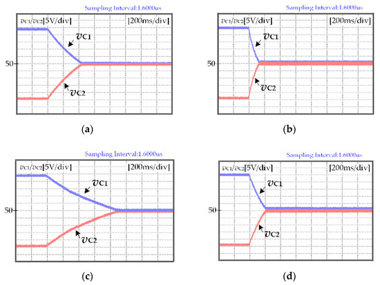
Figure 16.
Capacitor voltage waveforms during the transition of the NPV balance control. (a) m = 0.3, cos θ = 0.954; (b) m = 0.8, cos θ = 0.954; (c) m = 0.3, cos θ = 0.732; (d) m = 0.3, cos θ = 0.732.
6. Conclusions
A carrier-based DPWM strategy of the NPC three-level inverter is proposed in this paper. This strategy can be used in NPC three-level inverters for industrial applications, such as traction inverters in rail transit systems and mine hoist systems, where lower common-mode voltage and lower switching loss are required.
Firstly, the reference voltage is modified by two injections of the zero-sequence voltage. The DC-link voltage utilization of the inverter is enhanced by the first injection of the zero-sequence voltage. Then, the three phases are clamped alternatively to reduce the CMV and the switching loss by the second injection of the zero-sequence voltage. Secondly, the carrier is modified by phase opposition disposition to reduce the extra switches during the transition of two adjacent regions. Finally, without the change of switching sequence in each carrier period, the NPV balance is achieved by the injection of compensation voltage into the reference voltage. In addition, the output harmonic distortion is also improved by the proposed strategy.
Author Contributions
Conceptualization, G.Z. and Q.G.; methodology, G.Z. and Z.Z.; software, Y.S.; validation, Y.S.; formal analysis, Z.Z.; investigation, Q.G.; resources, G.Z.; data curation, Y.S.; writing—original draft preparation, Y.S.; writing—review and editing, G.Z.; visualization, Y.S.; supervision, Q.G.; project administration, Q.G.; funding acquisition, G.Z., Q.G. and Z.Z. All authors have read and agreed to the published version of the manuscript.
Funding
This research was funded by “The National Natural Science Foundation of China, grant number 51807140 and 52077154” and “The Natural Science Foundation of Tianjin City, grant number 20JCQNJC00030”.
Conflicts of Interest
The authors declare no conflict of interest.
References
- Rodriguez, J.; Bernet, S.; Steimer, P.K.; Lizama, I.E. A Survey on Neutral-Point-Clamped Inverters. IEEE Trans. Ind. Electron. 2010, 57, 2219–2230. [Google Scholar] [CrossRef]
- Kouro, S.; Malinowski, M.; Gopakumar, K.; Pou, J.; Franquelo, L.G.; Wu, B.; Rodriguez, J.; Perez, M.A.; Leon, J.I. Recent ad-vances and industrial applications of multilevel converters. IEEE Trans. Ind. Electron. 2010, 57, 2553–2580. [Google Scholar] [CrossRef]
- Abu-Rub, H.; Holtz, J.; Rodriguez, J.; Ge, B. Medium-voltage multilevel converters-state of the art, challenges, and requirements in industrial applications. IEEE Trans. Ind. Electron. 2010, 57, 2581–2596. [Google Scholar] [CrossRef]
- Yang, Y.; Wen, H.; Fan, M.; Xie, M.; Peng, S.; Norambuena, M.; Rodriguez, J. Computation-Efficient Model Predictive Control with Common-Mode Voltage Elimination for Five-Level ANPC Converters. IEEE Trans. Transp. Electrif. 2020, 6, 970–984. [Google Scholar] [CrossRef]
- Yu, B.; Song, W.; Guo, Y. Virtual Voltage Vectors Based Model Predictive Current Control for Five-Phase VSIs with Common-Mode Voltage Reduction. IEEE Trans. Transport. Electrif. 2021, 7, 706–717. [Google Scholar] [CrossRef]
- Guo, X.; Yang, Y.; Wang, B. Leakage Current Reduction of Three-Phase Z-Source Three-Level Four-Leg Inverter for Transformerless PV System. IEEE Trans. Power Electron. 2019, 34, 6299–6308. [Google Scholar] [CrossRef]
- Li, X.; Xing, X.; Zhang, C.; Chen, A.; Qin, C.; Zhang, G. Simultaneous Common-Mode Resonance Circulating Current and Leakage Current Suppression for Transformerless Three-Level T-Type PV Inverter System. IEEE Trans. Ind. Electron. 2019, 66, 4457–4467. [Google Scholar] [CrossRef]
- Dagan, K.J.; Zuckerberger, A.; Rabinovici, R. Fourth-Arm Common-Mode Voltage Mitigation. IEEE Trans. Power Electron. 2016, 31, 1401–1407. [Google Scholar] [CrossRef]
- Ohn, S.; Yu, J.; Burgos, R. Reduced Common-Mode Voltage PWM Scheme for Full-SiC Three-level Uninterruptible Power Supply with Small DC-link Capacitors. IEEE Trans. Power Electron. 2020, 35, 8638–8651. [Google Scholar] [CrossRef]
- Xiao, H.; Xie, S. Transformerless Split-Inductor Neutral Point Clamped Three-Level PV Grid-Connected Inverter. IEEE Trans. Power Electron. 2011, 27, 1799–1808. [Google Scholar] [CrossRef]
- Hizarci, H.; Pekperlak, U.; Arifoglu, U. Conducted Emission Suppression Using an EMI Filter for Grid-Tied Three-Phase/Level T-Type Solar Inverter. IEEE Access 2021, 9, 67417–67431. [Google Scholar] [CrossRef]
- Jung, J.-H.; Hwang, S.-I.; Kim, J.-M. A Common-Mode Voltage Reduction Method Using an Active Power Filter for a Three-Phase Three-Level NPC PWM Converter. IEEE Trans. Ind. Appl. 2021, 57, 3787–3800. [Google Scholar] [CrossRef]
- Wu, K.; Xia, C.L.; Zhang, Y. Common-Mode Voltage Suppression for Neutral Point Clamped Three Level Inverter. Trans. China Electrotech. Soc. 2015, 30, 110–117. [Google Scholar]
- Nguyen, T.T.; Nguyen, N. An Efficient Four-State Zero Common-Mode Voltage PWM Scheme with Reduced Current Distortion for a Three-Level Inverter. IEEE Trans. Ind. Electron. 2018, 65, 1021–1030. [Google Scholar] [CrossRef]
- Liu, P.; Duan, S.; Yao, C.; Chen, C. A Double Modulation Wave CBPWM Strategy Providing Neutral-Point Voltage Oscillation Elimination and CMV Reduction for Three-Level NPC Inverters. IEEE Trans. Ind. Electron. 2017, 65, 16–26. [Google Scholar] [CrossRef]
- Xing, X.; Li, X.; Gao, F.; Qin, C.; Zhang, C. Improved Space Vector Modulation Technique for Neutral-Point Voltage Oscillation and Common-Mode Voltage Reduction in Three-Level Inverter. IEEE Trans. Power Electron. 2019, 34, 8697–8714. [Google Scholar] [CrossRef]
- Jiang, W.; Wang, P.; Ma, M.; Wang, J.; Li, J.; Li, L.; Chen, K. A Novel Virtual Space Vector Modulation with Reduced Common-Mode Voltage and Eliminated Neutral Point Voltage Oscillation for Neutral Point Clamped Three-Level Inverter. IEEE Trans. Ind. Electron. 2020, 67, 884–894. [Google Scholar] [CrossRef]
- Gao, Z.; Li, Y.; Ge, Q. Improved Phase Opposition Disposition Pulse Width Modulation Strategy for Three Level Neutral Point Clamped Converter. Trans. China Electrotech. Soc. 2020, 35, 884–894. [Google Scholar]
- Scognamillo, C.; Catalano, A.; Riccio, M.; D’Alessandro, V.; Codecasa, L.; Borghese, A.; Tripathi, R.; Castellazzi, A.; Breglio, G.; Irace, A. Compact Modeling of a 3.3 kV SiC MOSFET Power Module for Detailed Circuit-Level Electrothermal Simulations Including Parasitics. Energies 2021, 14, 4683. [Google Scholar] [CrossRef]
- Catalano, A.P.; Scognamillo, C.; D’Alessandro, V.; Castellazzi, A. Numerical Simulation and Analytical Modeling of the Thermal Behavior of Single- and Double-Sided Cooled Power Modules. IEEE Trans. Compon. Packag. Manuf. Technol. 2020, 10, 1446–1453. [Google Scholar] [CrossRef]
- Riccio, J.; Odhano, S.A.; Zanchetta, P. Sensorless and Modulated Model-Predictive Control for a Doubly Fed Induction Machine. In Proceedings of the 2019 21st European Conference on Power Electronics and Applications (EPE ’19 ECCE Europe), Genova, Italy, 3–5 September 2019. [Google Scholar]
- McGrath, B.; Holmes, D.; Lipo, T. Optimized space vector switching sequences for multilevel inverters. IEEE Trans. Power Electron. 2003, 18, 1293–1301. [Google Scholar] [CrossRef]
- Xia, C.; Zhang, G.; Yan, Y.; Gu, X.; Shi, T.; He, X. Discontinuous Space Vector PWM Strategy of Neutral-Point-Clamped Three-Level Inverters for Output Current Ripple Reduction. IEEE Trans. Power Electron. 2016, 32, 5109–5121. [Google Scholar] [CrossRef]
Publisher’s Note: MDPI stays neutral with regard to jurisdictional claims in published maps and institutional affiliations. |
© 2021 by the authors. Licensee MDPI, Basel, Switzerland. This article is an open access article distributed under the terms and conditions of the Creative Commons Attribution (CC BY) license (https://creativecommons.org/licenses/by/4.0/).