
Printed Split-Ring Loops with High Q-Factor for Wireless Power Transmission

 ,
, 


Abstract
:1. Introduction
2. Principle of Planar Split-Ring Loops
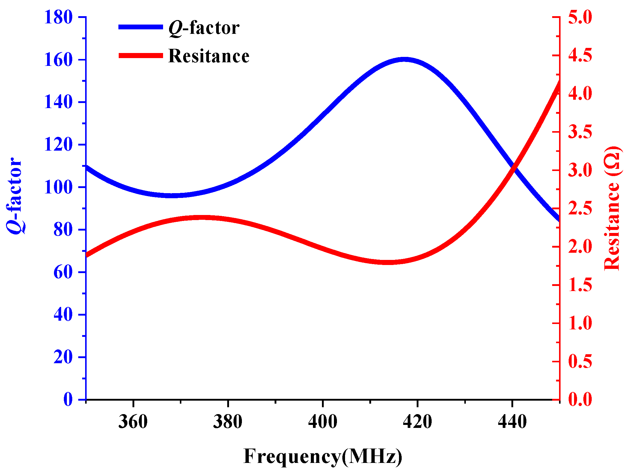
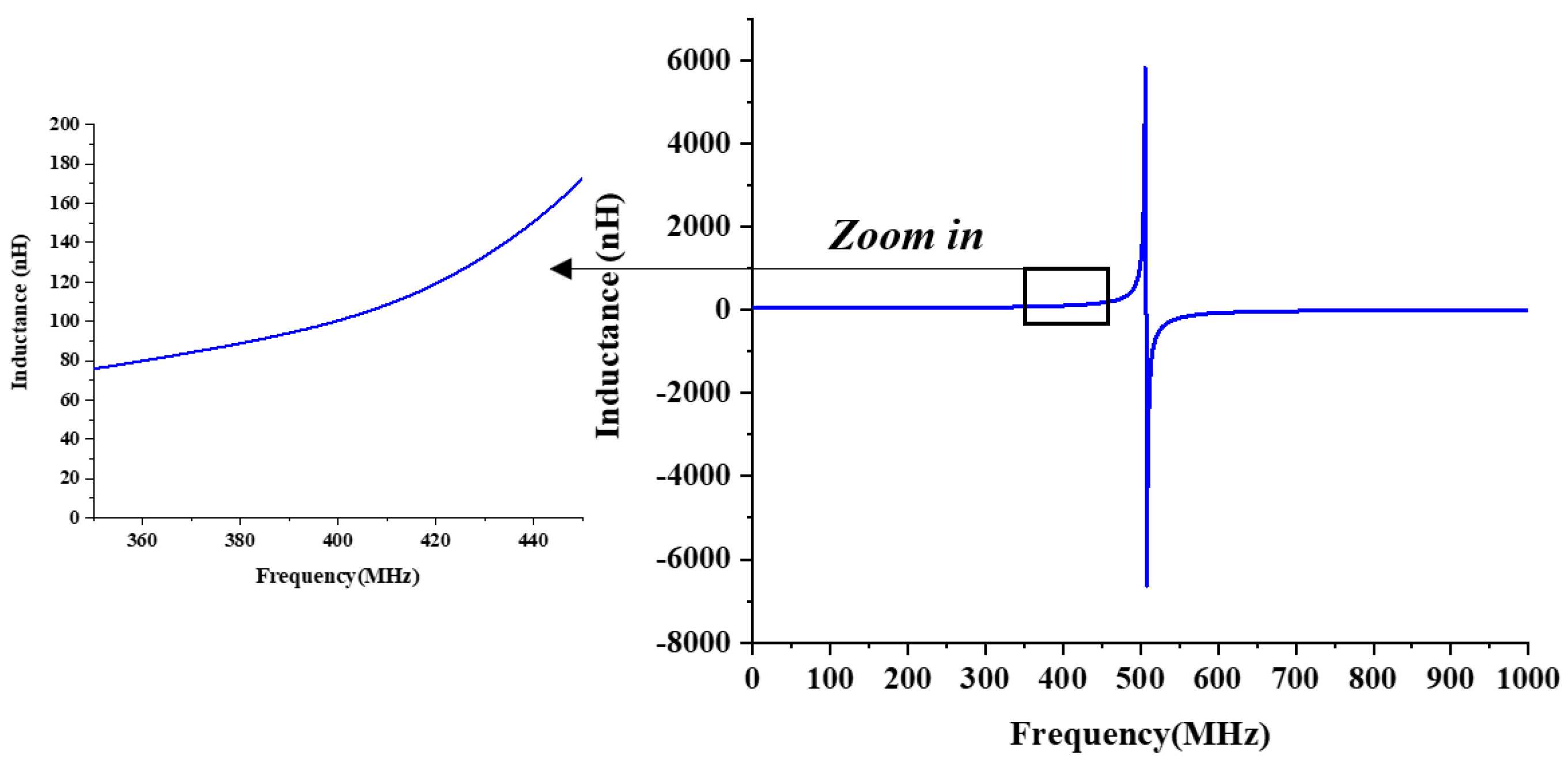
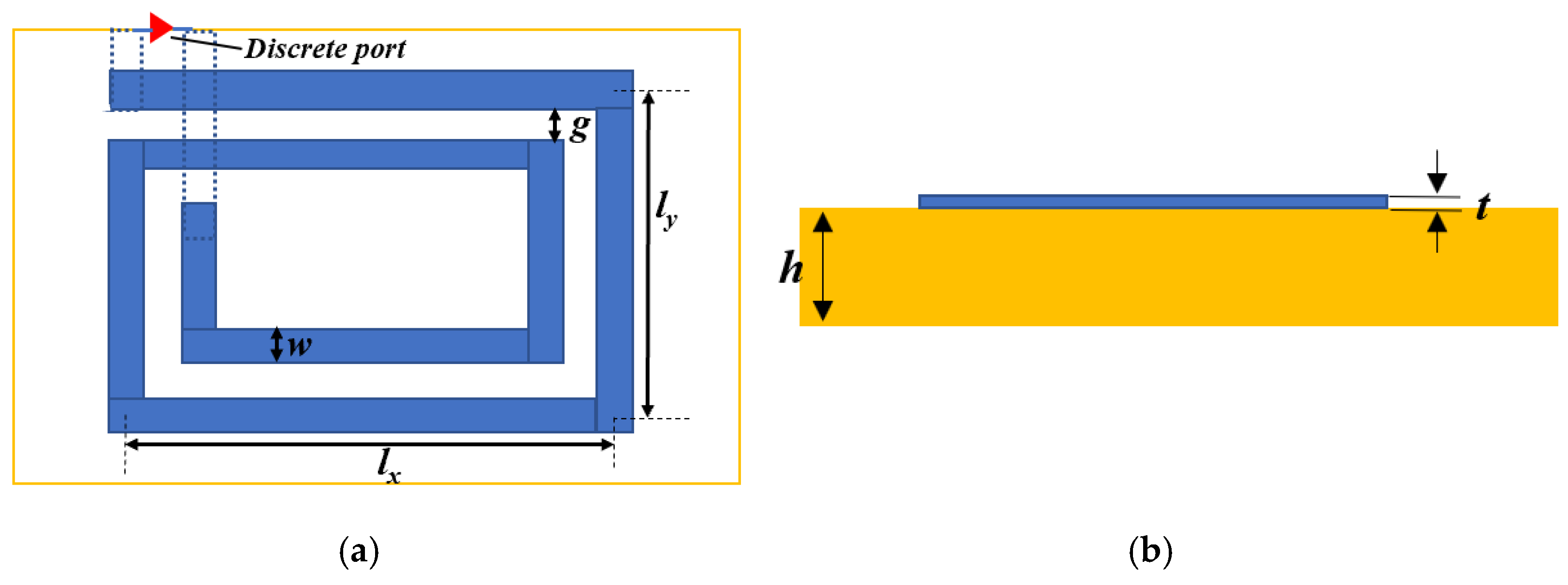
2.1. A Conventional Rectangular Planar Spiral Coil
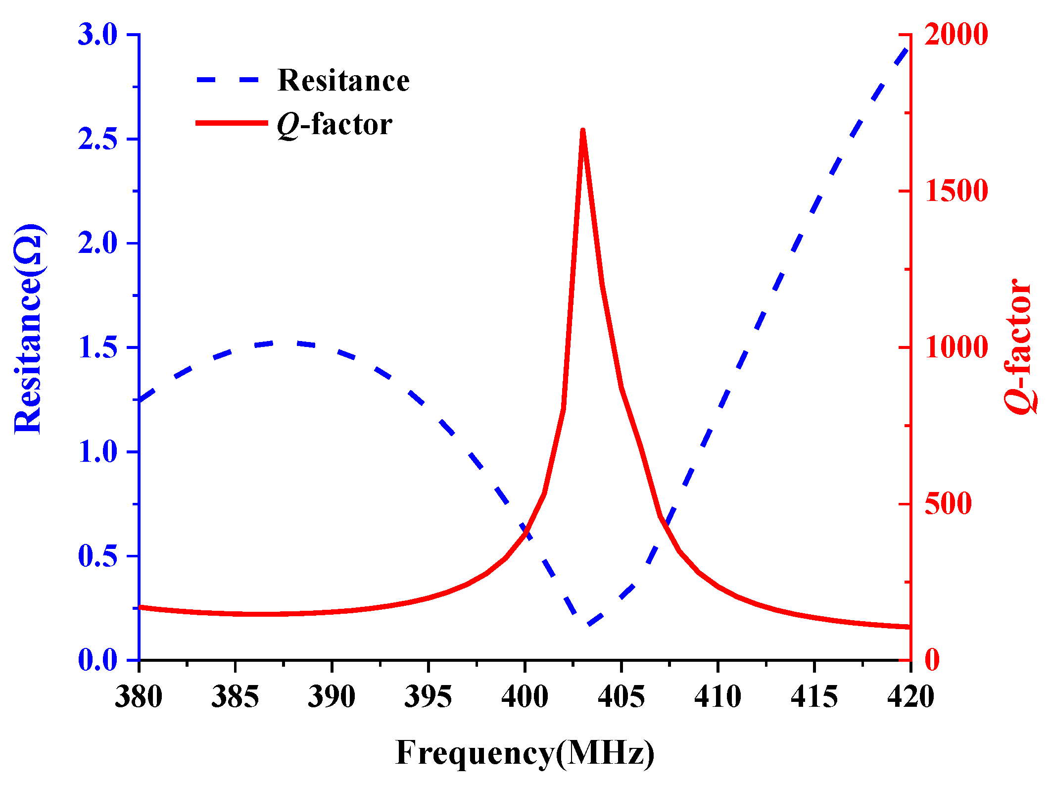
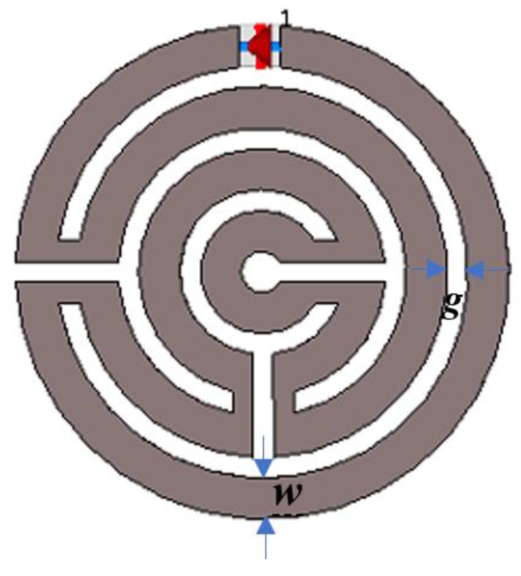
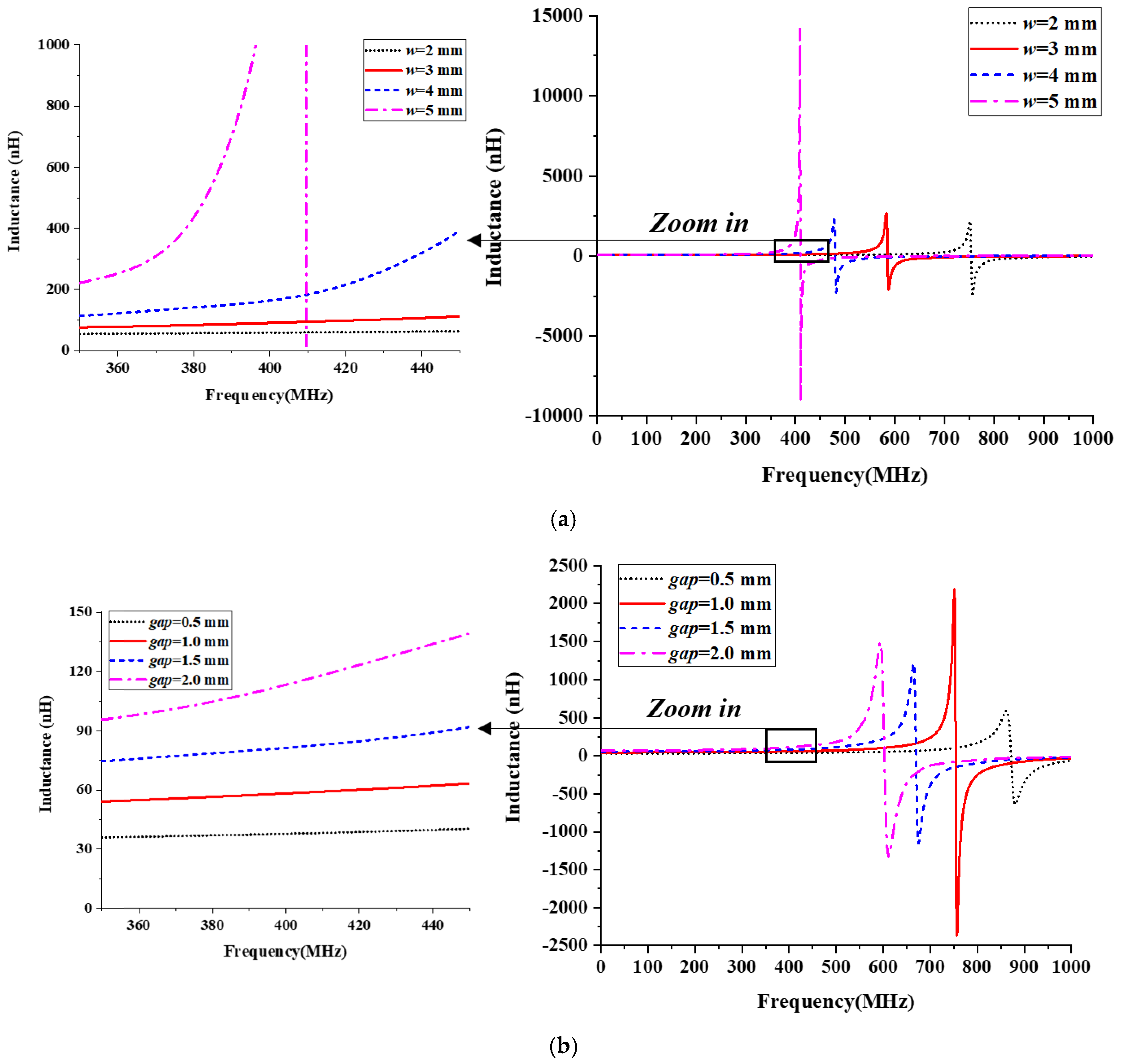
2.2. A Planar Split-Ring Loop
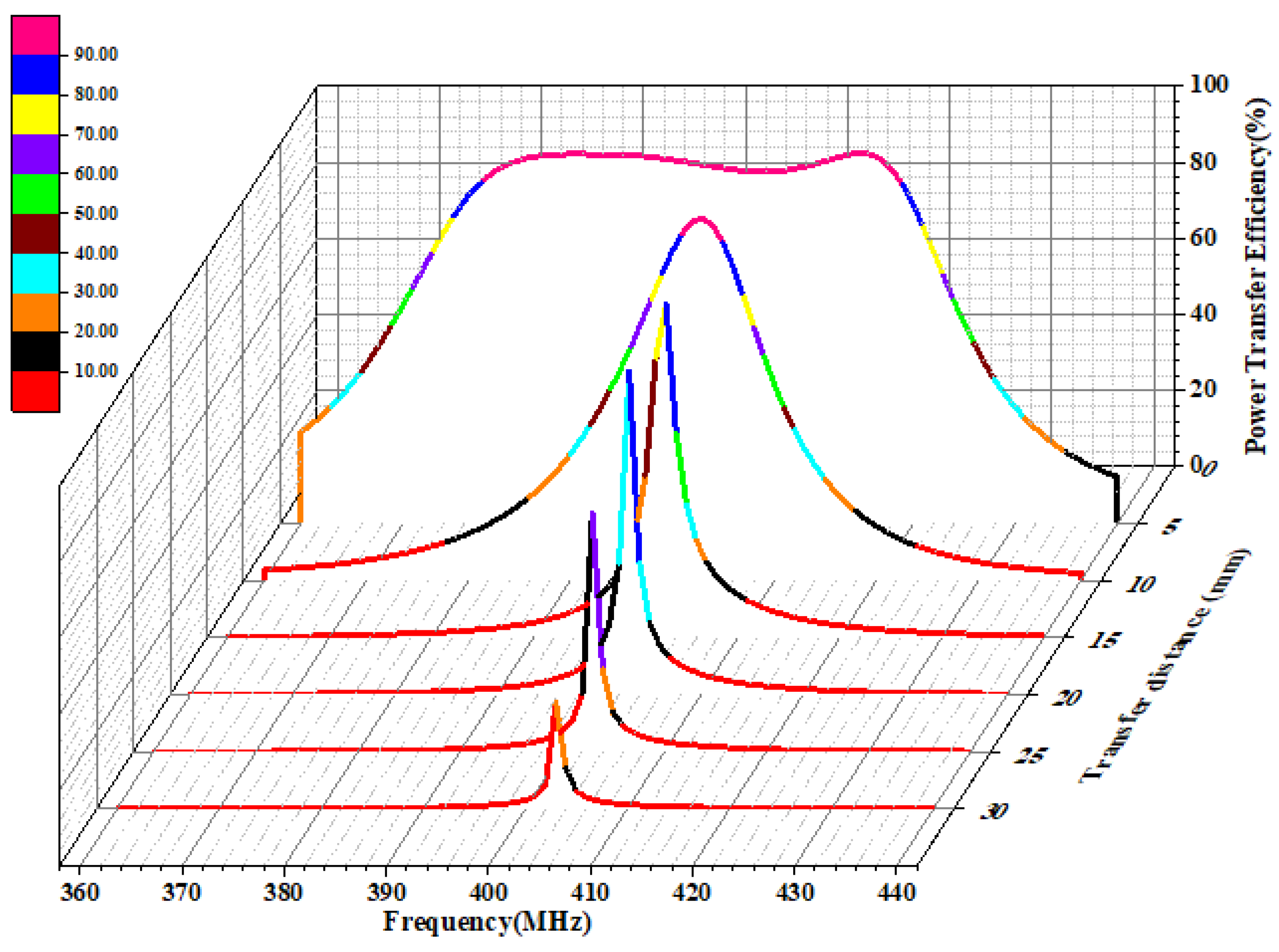
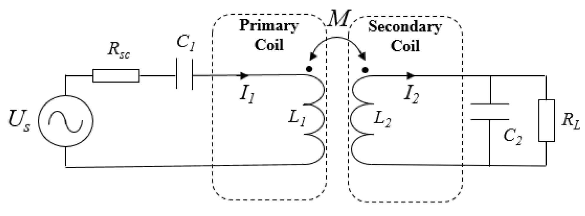
3. Performance of the WPT Link Using Planar Split-Ring Loop
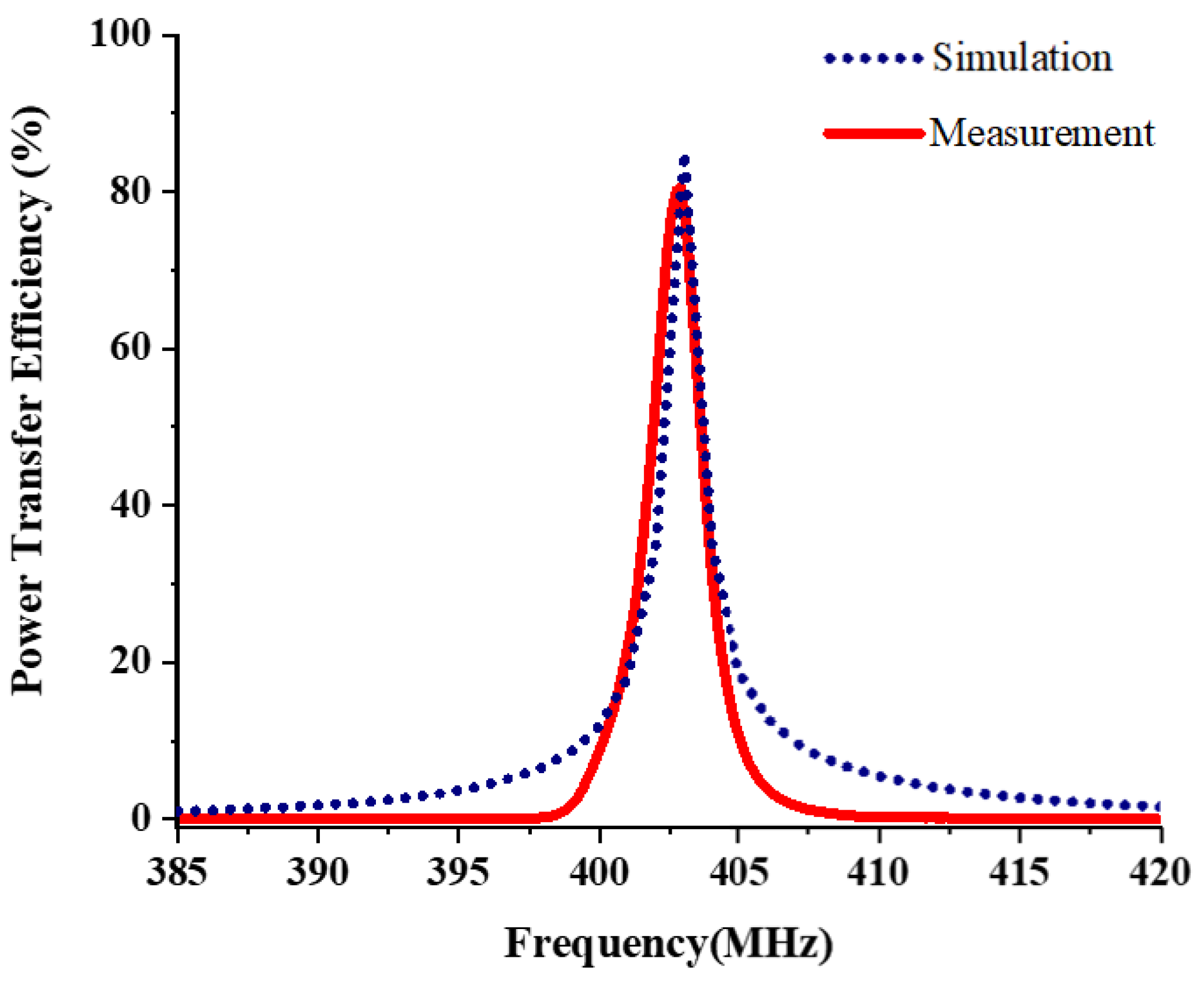
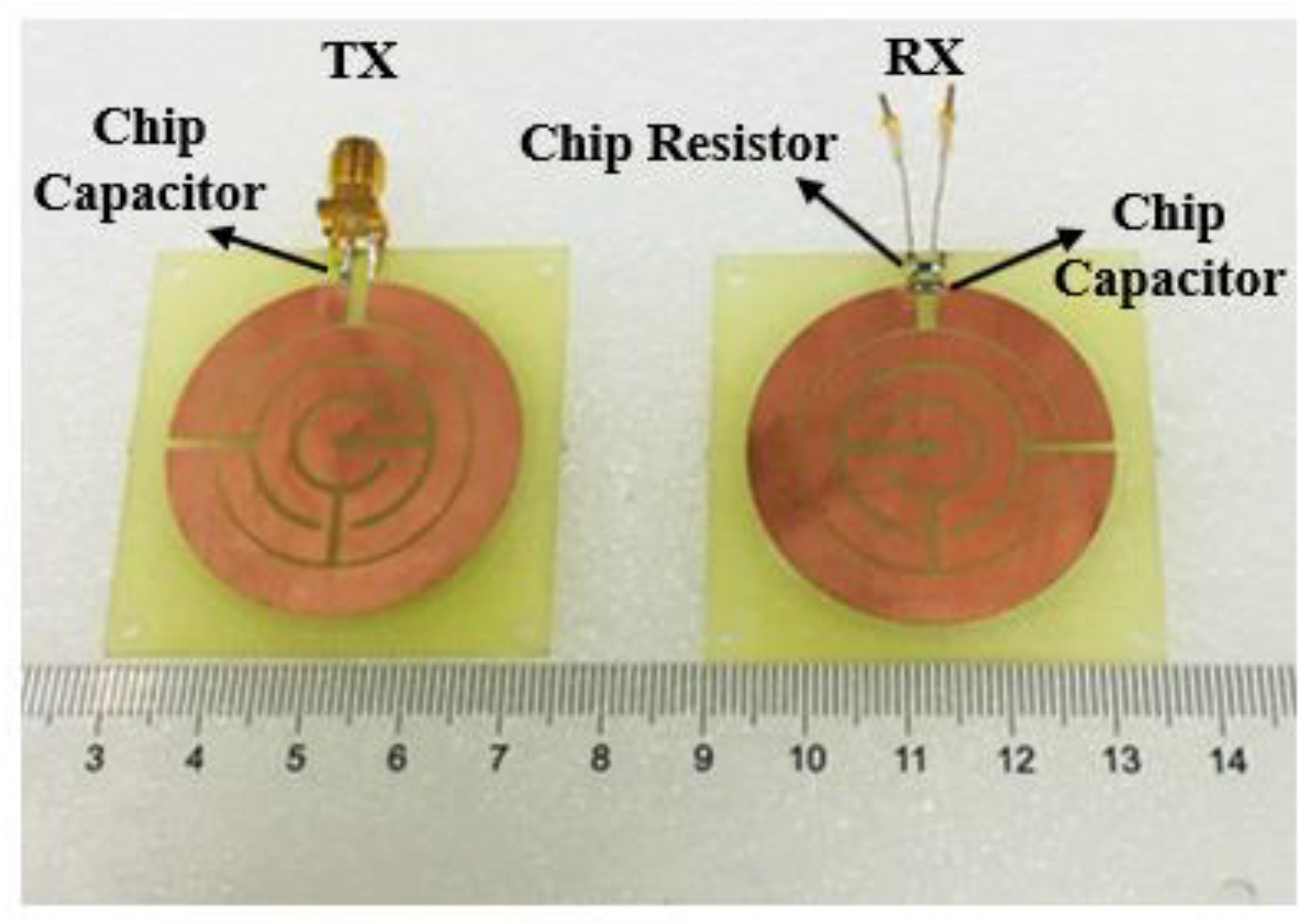
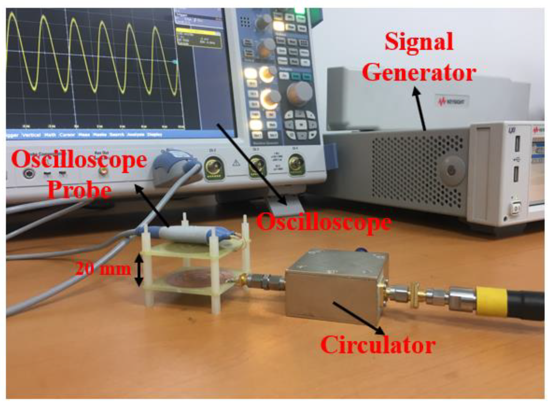
4. Measurement
5. Conclusions
Author Contributions
Funding
Institutional Review Board Statement
Informed Consent Statement
Data Availability Statement
Acknowledgments
Conflicts of Interest
References
- Jiang, Z.; Wang, Z.; Leach, M.; Lim, E.G.; Wang, J.; Pei, R.; Huang, Y. Wideband Loop Antenna with Split-Ring Resonators for Wireless Medical Telemetry. IEEE Antennas Wirel. Propag. Lett. 2019, 18, 1415–1419. [Google Scholar] [CrossRef]
- Wang, J.; Lim, E.G.; Leach, M.; Wang, Z.; Man, K.L.; Huang, Y. Review of Wearable Antennas for WBAN Applications. IAENG Int. J. Comput. Sci. 2016, 43, 474–480. [Google Scholar]
- Lim, E.; Wang, Z.; Yu, F.Z.; Tillo, T.; Man, K.L.; Wang, J.C.; Zhang, M. Transmitter antennas for wireless capsule endoscopy. In Proceedings of the 2012 International SoC Design Conference (ISOCC), Jeju, Korea, 4–7 November 2012; pp. 269–272. [Google Scholar]
- Dinis, H.; Colmiais, I.; Mendes, P.M. Extending the Limits of Wireless Power Transfer to Miniaturized Implantable Electronic Devices. Micromachines 2017, 8, 359. [Google Scholar] [CrossRef] [PubMed] [Green Version]
- Hui, S.Y.R. Planar Wireless Charging Technology for Portable Electronic Products and Qi. Proc. IEEE 2013, 101, 1290–1301. [Google Scholar] [CrossRef] [Green Version]
- Popovic, Z. Cut the Cord: Low-Power Far-Field Wireless Powering. IEEE Microw. Mag. 2013, 14, 55–62. [Google Scholar] [CrossRef]
- Ho, S.L.; Wang, J.; Fu, W.; Sun, M. A Comparative Study Between Novel Witricity and Traditional Inductive Magnetic Coupling in Wireless Charging. IEEE Trans. Magn. 2011, 47, 1522–1525. [Google Scholar] [CrossRef]
- Kurs, A.; Karalis, A.; Moffatt, R.; Joannopoulos, J.D.; Fisher, P.; Soljačic, M. Wireless Power Transfer via Strongly Coupled Magnetic Resonances. Science 2007, 317, 83–86. [Google Scholar] [CrossRef] [PubMed] [Green Version]
- Lu, F.; Zhang, H.; Mi, C. A Review on the Recent Development of Capacitive Wireless Power Transfer Technology. Energies 2017, 10, 1752. [Google Scholar] [CrossRef] [Green Version]
- Khan, S.R.; Choi, G. Analysis and Optimization of Four-Coil Planar Magnetically Coupled Printed Spiral Resonators. Sensors 2016, 16, 1219. [Google Scholar] [CrossRef] [PubMed] [Green Version]
- Jolani, F.; Yu, Y.; Chen, Z. A Planar Magnetically Coupled Resonant Wireless Power Transfer System Using Printed Spiral Coils. IEEE Antennas Wirel. Propag. Lett. 2014, 13, 1648–1651. [Google Scholar] [CrossRef]
- Falavarjani, M.M.; Shahabadi, M.; Rashed-Mohassel, J. Design and Implementation of Compact WPT link using Printed Spiral Resonators. Electron. Lett. 2014, 50, 110–111. [Google Scholar] [CrossRef]
- Mehri, S.; Ammari, A.C.; Slama, J.B.H.; Rmili, H. Geometry Optimization Approaches of Inductively Coupled Printed Spiral Coils for Remote Powering of Implantable Biomedical Sensors. J. Sens. 2016, 2016, 4869571. [Google Scholar] [CrossRef]
- Wang, J.; Leach, M.; Lim, E.; Wang, Z.; Huang, Y. Wireless Power Transfer Using Resonance Coupling Method for Implantable Applications. In Proceedings of the 2018 IEEE International Symposium on Antennas and Propagation & USNC/URSI National Radio Science Meeting, Boston, MA, USA, 8–13 July 2018; pp. 2557–2558. [Google Scholar]
- Javidi, F.N.; Nymand, M. A New Method for Measuring Winding AC Resistance of High-Efficiency Power Inductors. IEEE Trans. Power Electron. 2018, 33, 10736–10747. [Google Scholar] [CrossRef]
- Sathyasree, J.; Vanukuru, V.; Nair, D.; Chakravorty, A. Compact Modeling of Proximity Effect in High-Q Tapered Spiral Inductors. IEEE Electron Device Lett. 2018, 39, 588–590. [Google Scholar] [CrossRef]
- Lawson, J.; Yates, D.C.; Mitcheson, P.D. High Q Coil Measurement for Inductive Power Transfer. IEEE Trans. Microw. Theory Tech. 2019, 67, 1962–1973. [Google Scholar] [CrossRef]
- Wang, J.; Leach, M.; Lim, E.; Wang, Z.; Huang, Y. Investigation of magnetic resonance coupling circuit topologies for wireless power transmission. Microw. Opt. Technol. Lett. 2019, 61, 1755–1763. [Google Scholar] [CrossRef]
- Duan, Z.; Guo, Y.; Kwong, D.-L. Rectangular coils optimization for wireless power transmission. Radio Sci. 2012, 47, RS2013. [Google Scholar] [CrossRef]
- Kim, S.; Bae, B.; Kong, S.; Jung, D.H.; Kim, J.J.; Kim, J. Design, implementation and measurement of board-to-board wireless power transfer (WPT) for low voltage applications. In Proceedings of the 2013 IEEE 22nd Conference on Electrical Performance of Electronic Packaging and Systems, Austin, TX, USA, 27–13 October 2013; pp. 91–95. [Google Scholar]
- Wang, J.; Leach, M.P.; Lim, E.; Wang, Z.; Jiang, Z.; Pei, R.; Huang, Y. A Conformal Split-Ring Loop as a Self-Resonator for Wireless Power Transfer. IEEE Access 2019, 8, 911–919. [Google Scholar] [CrossRef]


| Parameters | w | g | lx | ly |
| Value (mm) | 0.48 | 0.17 | 10 | 8 |
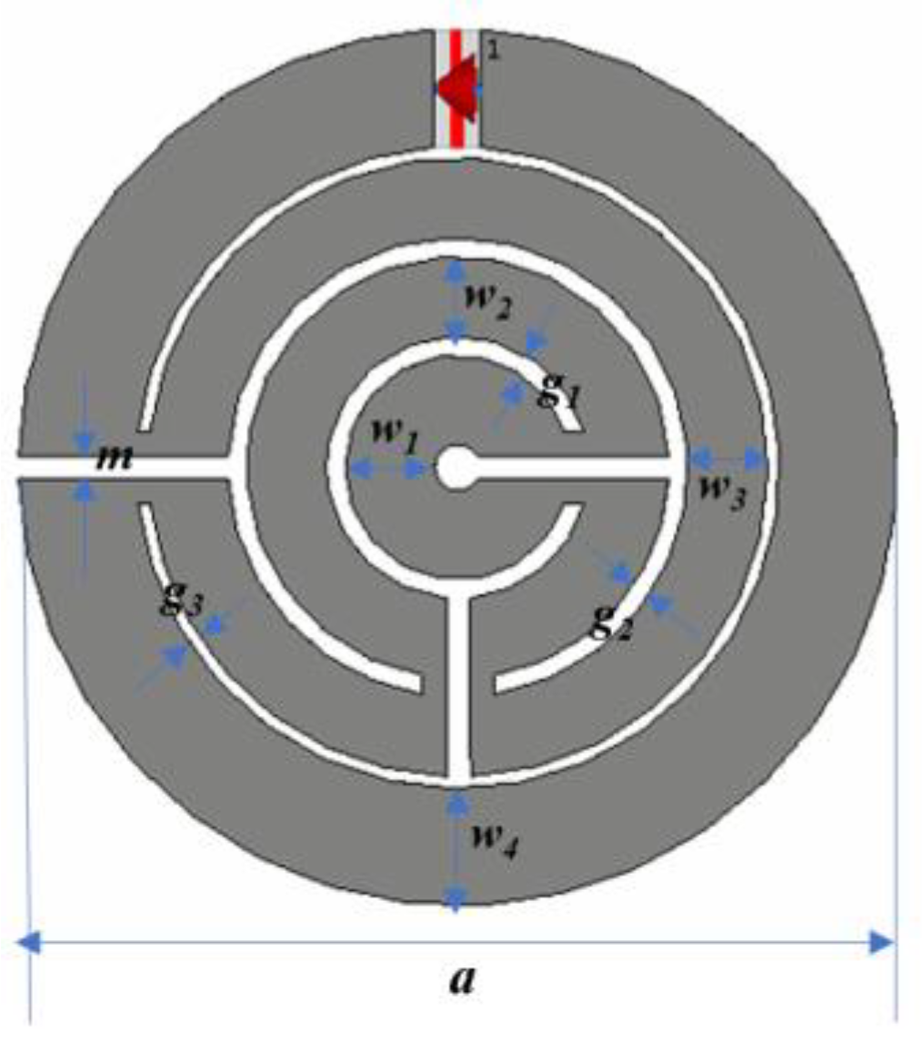
| Parameters | w1 | w2 | w3 | w4 | g1 | g2 | g3 | m | a |
| Value(mm) | 3.8 | 3.4 | 3.4 | 5.0 | 0.8 | 0.8 | 0.5 | 1.0 | 37.4 |
| Ref. | Coil Size (mm2) | Freq. (MHz) | Q-Factor | Inductance (nH) | Transfer Distance (mm) | Mutual Inductance (nH) | PTE |
|---|---|---|---|---|---|---|---|
| Rectangular PSC | 10.48 × 8.48 | 403 | 140 | 106 | 5 | 16.83 | 85.6% |
| Planar split-ring loop | 37.4 × 37.4 | 403 | 1630 | 106 | 10 | 7.37 | 95.3% |
| 20 | 3.26 | 85.1% |
| Ref. | Tx Coil Size (mm2) | Rx Coil Size (mm2) | Freq. (MHz) | Transfer Distance (mm) | Measured PTE |
|---|---|---|---|---|---|
| [19] | 60 × 24 | 25 × 10 | 3 | 10 | 46.4% |
| [20] | 10 × 10 | 10 × 10 | 110 | 3 | 30% (Simulated) |
| [21] | 45 × 45 | 45 × 45 | 433 | 22 | 87.9% |
| This work | 37.4 × 37.4 | 37.4 × 37.4 | 403 | 20 | 80.5% |
Publisher’s Note: MDPI stays neutral with regard to jurisdictional claims in published maps and institutional affiliations. |
© 2021 by the authors. Licensee MDPI, Basel, Switzerland. This article is an open access article distributed under the terms and conditions of the Creative Commons Attribution (CC BY) license (https://creativecommons.org/licenses/by/4.0/).
Share and Cite
Wang, J.; Leach, M.P.; Lim, E.G.; Wang, Z.; Pei, R.; Jiang, Z.; Huang, Y. Printed Split-Ring Loops with High Q-Factor for Wireless Power Transmission. Electronics 2021, 10, 2884. https://doi.org/10.3390/electronics10222884
Wang J, Leach MP, Lim EG, Wang Z, Pei R, Jiang Z, Huang Y. Printed Split-Ring Loops with High Q-Factor for Wireless Power Transmission. Electronics. 2021; 10(22):2884. https://doi.org/10.3390/electronics10222884
Chicago/Turabian StyleWang, Jingchen, Mark Paul Leach, Eng Gee Lim, Zhao Wang, Rui Pei, Zhenzhen Jiang, and Yi Huang. 2021. "Printed Split-Ring Loops with High Q-Factor for Wireless Power Transmission" Electronics 10, no. 22: 2884. https://doi.org/10.3390/electronics10222884
APA StyleWang, J., Leach, M. P., Lim, E. G., Wang, Z., Pei, R., Jiang, Z., & Huang, Y. (2021). Printed Split-Ring Loops with High Q-Factor for Wireless Power Transmission. Electronics, 10(22), 2884. https://doi.org/10.3390/electronics10222884