
Development of a 0.15 μm GaAs pHEMT Process Design Kit for Low-Noise Applications

 , ,
, ,  ,
,
Abstract
:1. Introduction
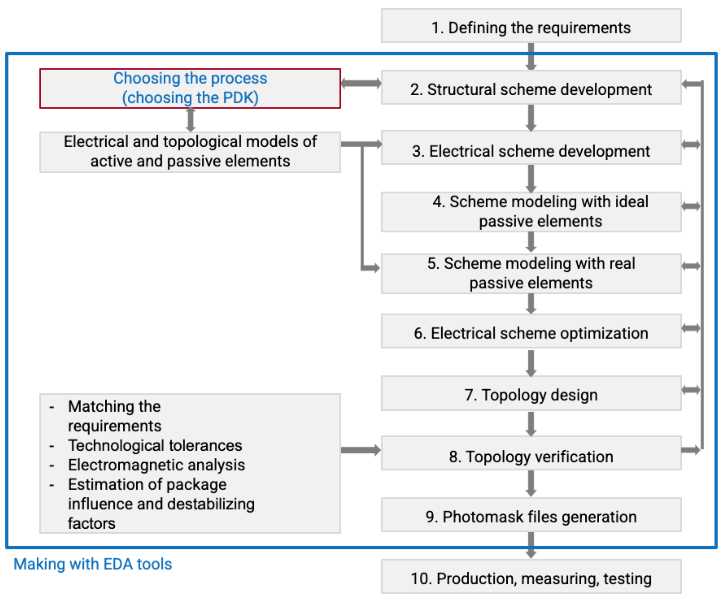
2. Materials and Methods
- Detailed study of the process and topological design rules;
- Design of topology templates for elements;
- Development of test structures for characterization of elements;
- Development of circuit fragments for initial verification of element models;
- Fabrication of test structures and circuit fragments;
- Measurement of test structures and circuit fragments, mathematical processing of measurement results;
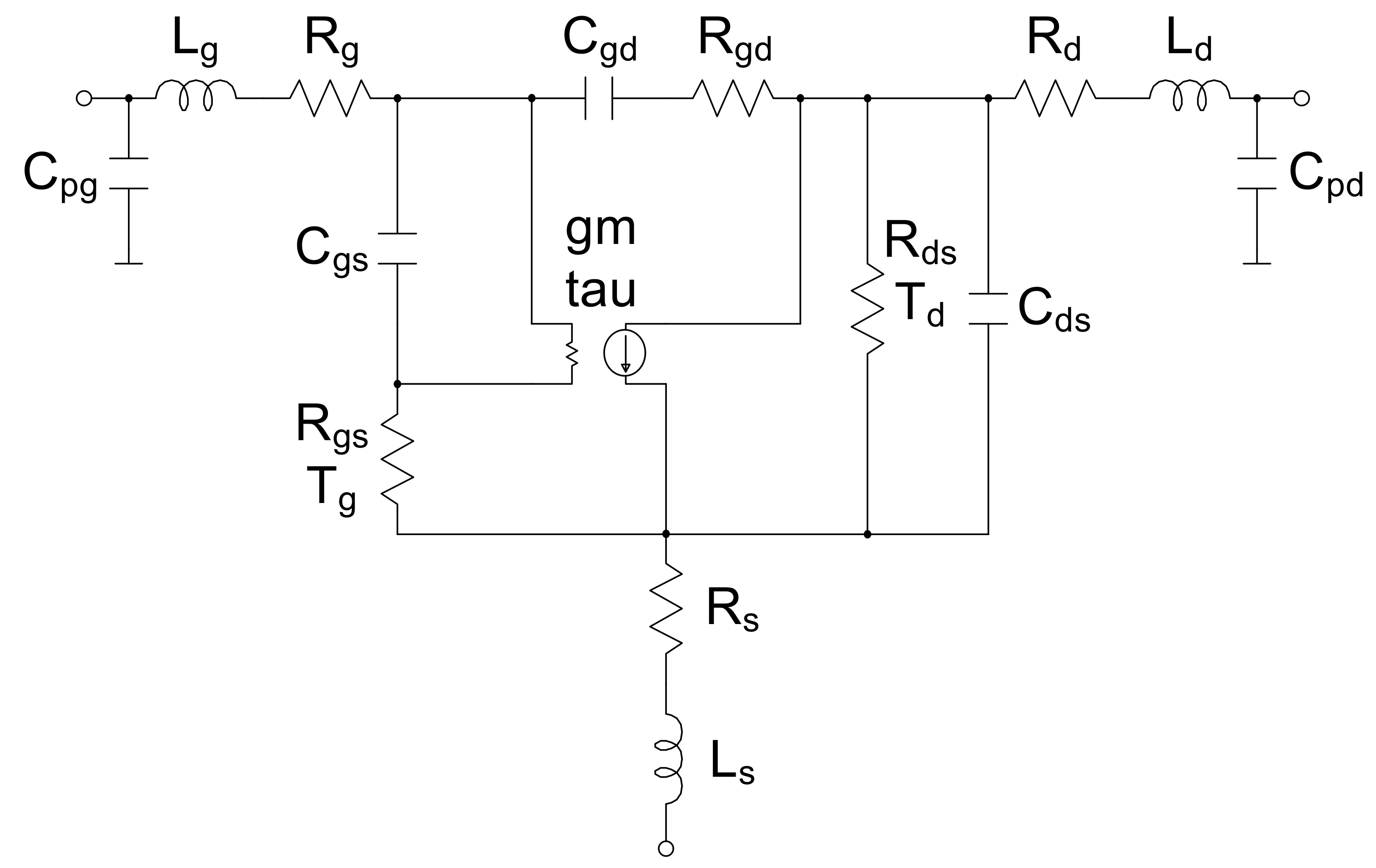
- Development of electrical and topological models of elements;
- Initial verification of element models;
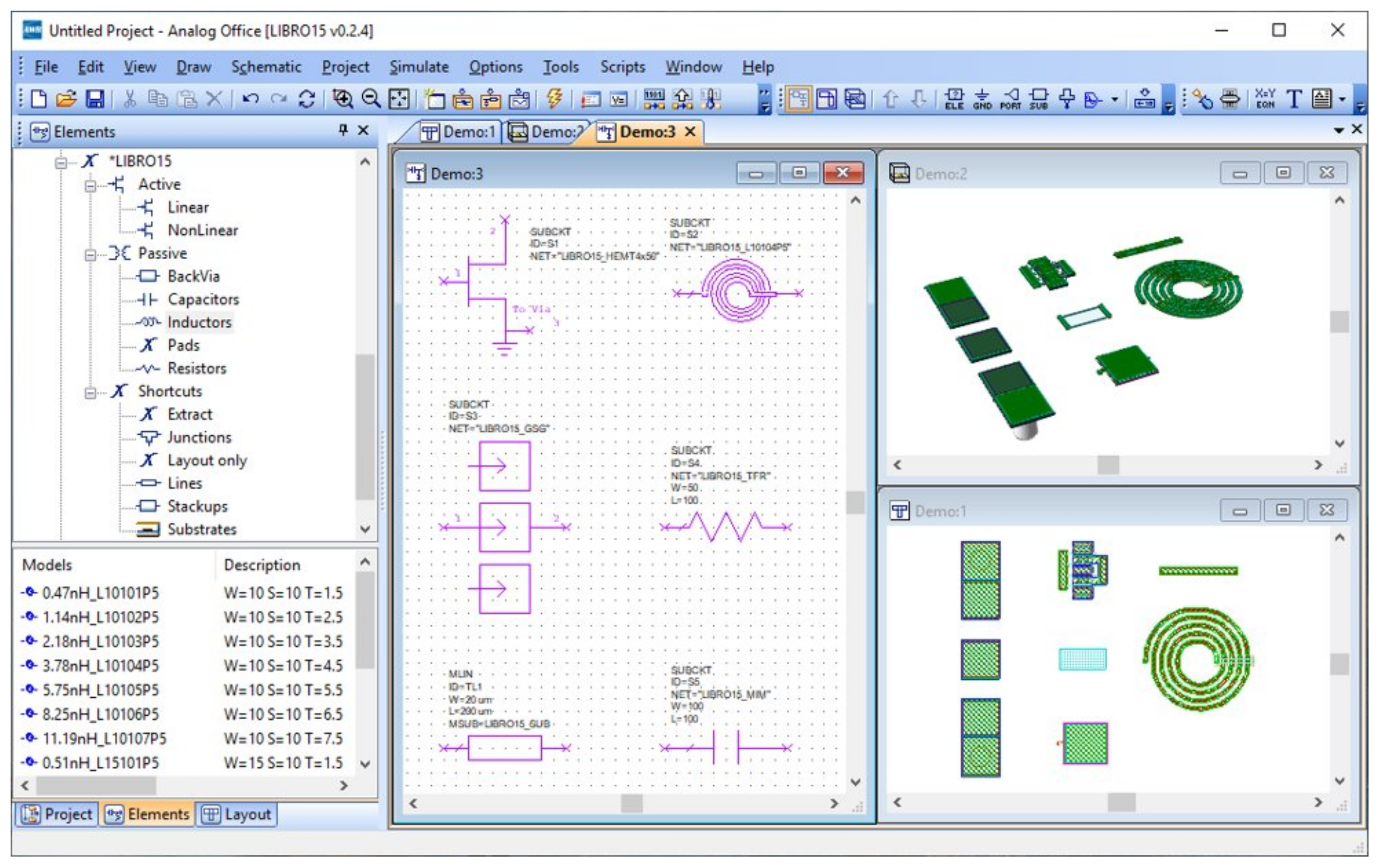
- Development of library structure of elements, setting up electromagnetic analysis and topology verification tools;
- Preparation of reference information;
- Release of the first version of PDK;
- Design of test microwave devices for validation of the first version of PDK.
3. Results
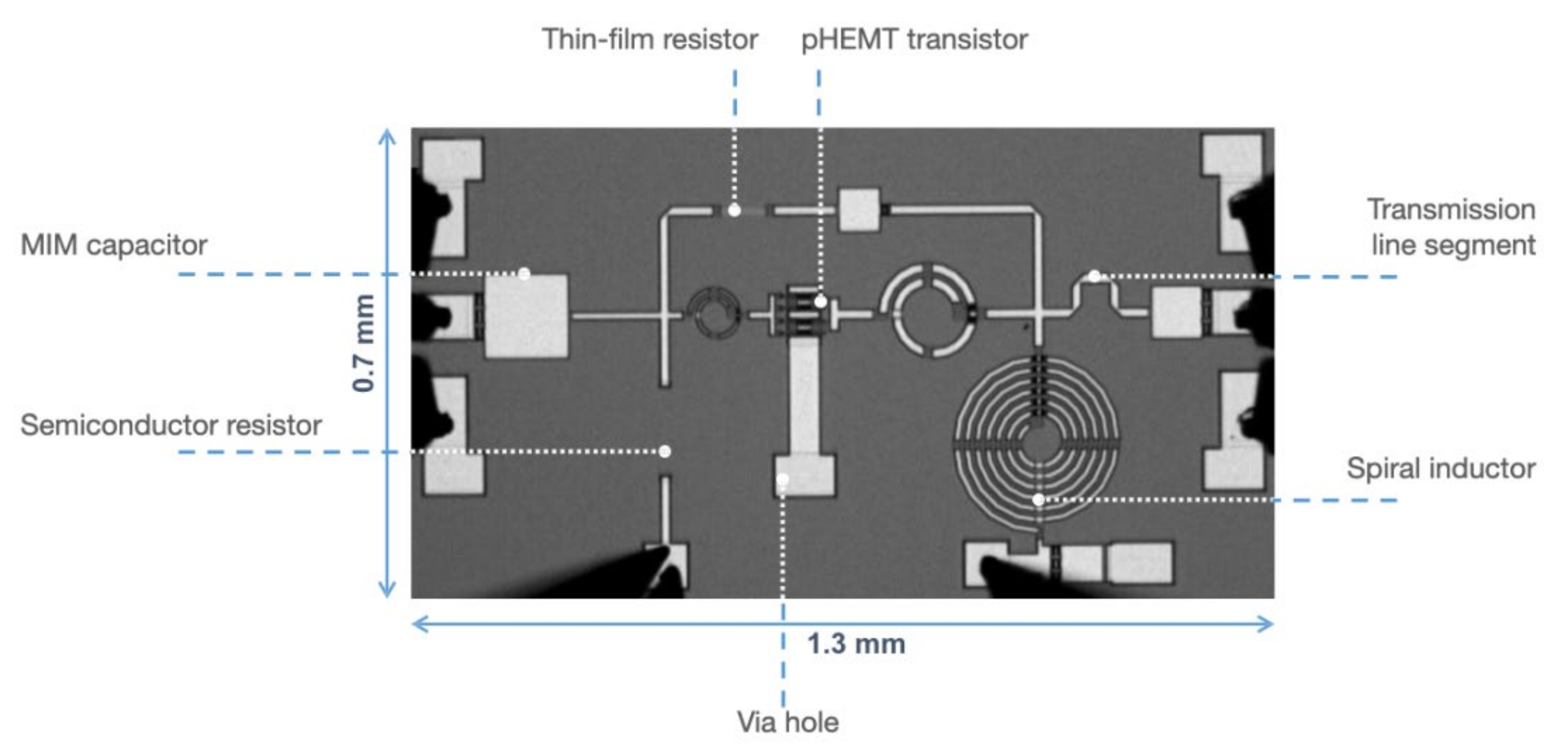
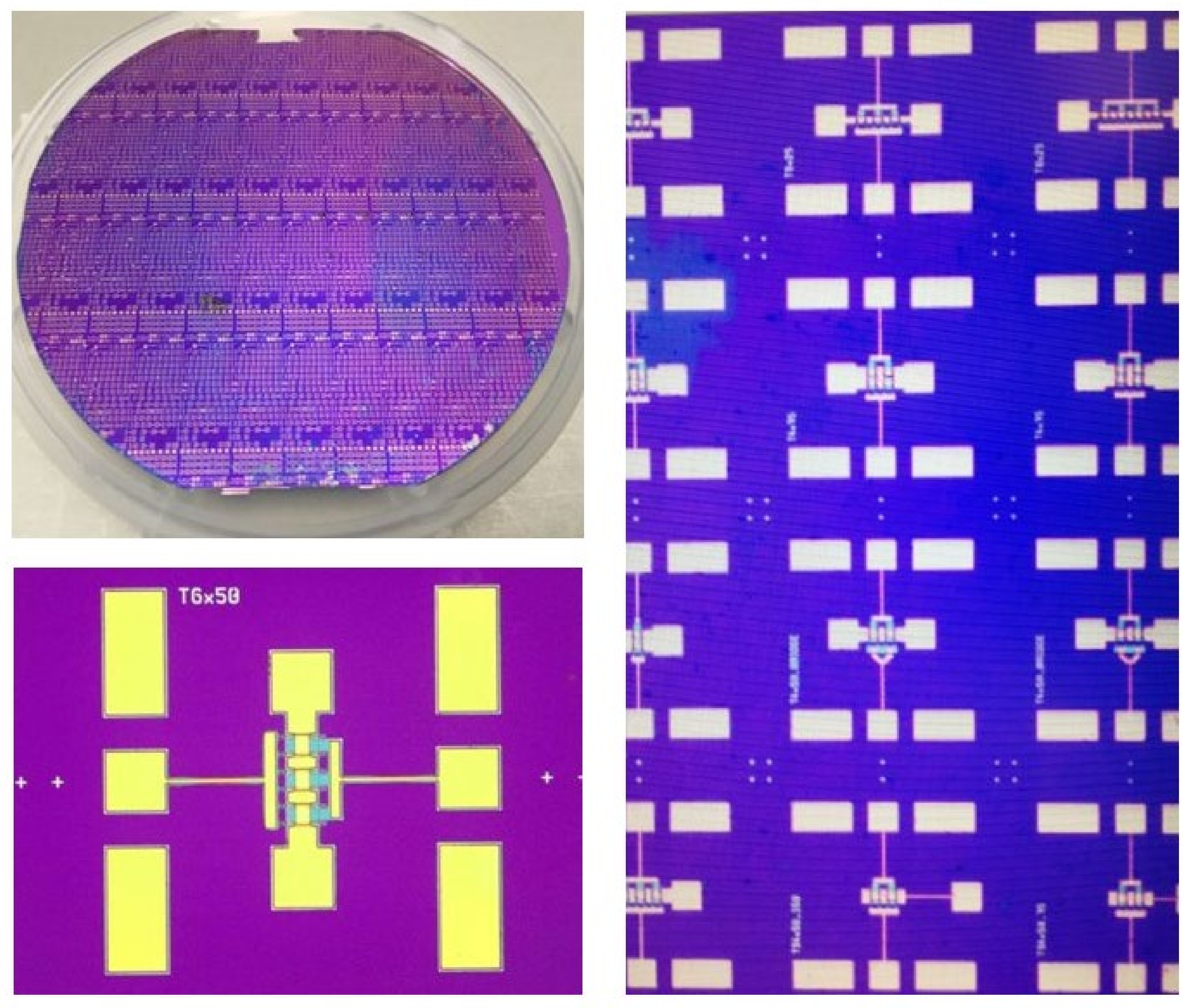
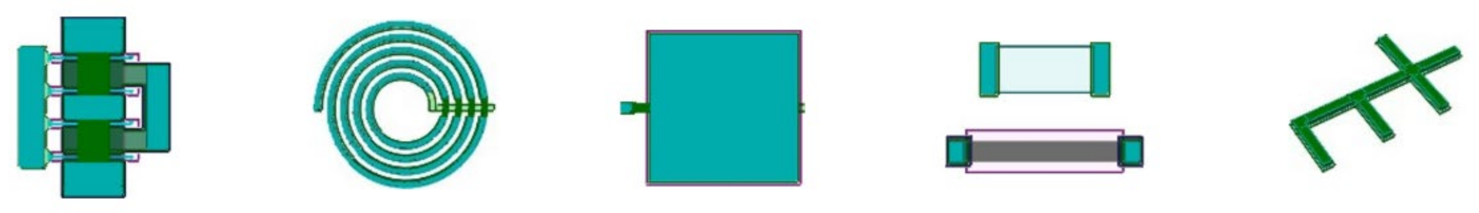
- Active elements;
- Passive elements;
- Transmission line segments;
- Structures for de-embedding;
- Fragments of circuits for verification of electromagnetic analysis;
- Process control monitor (PCM) tests.
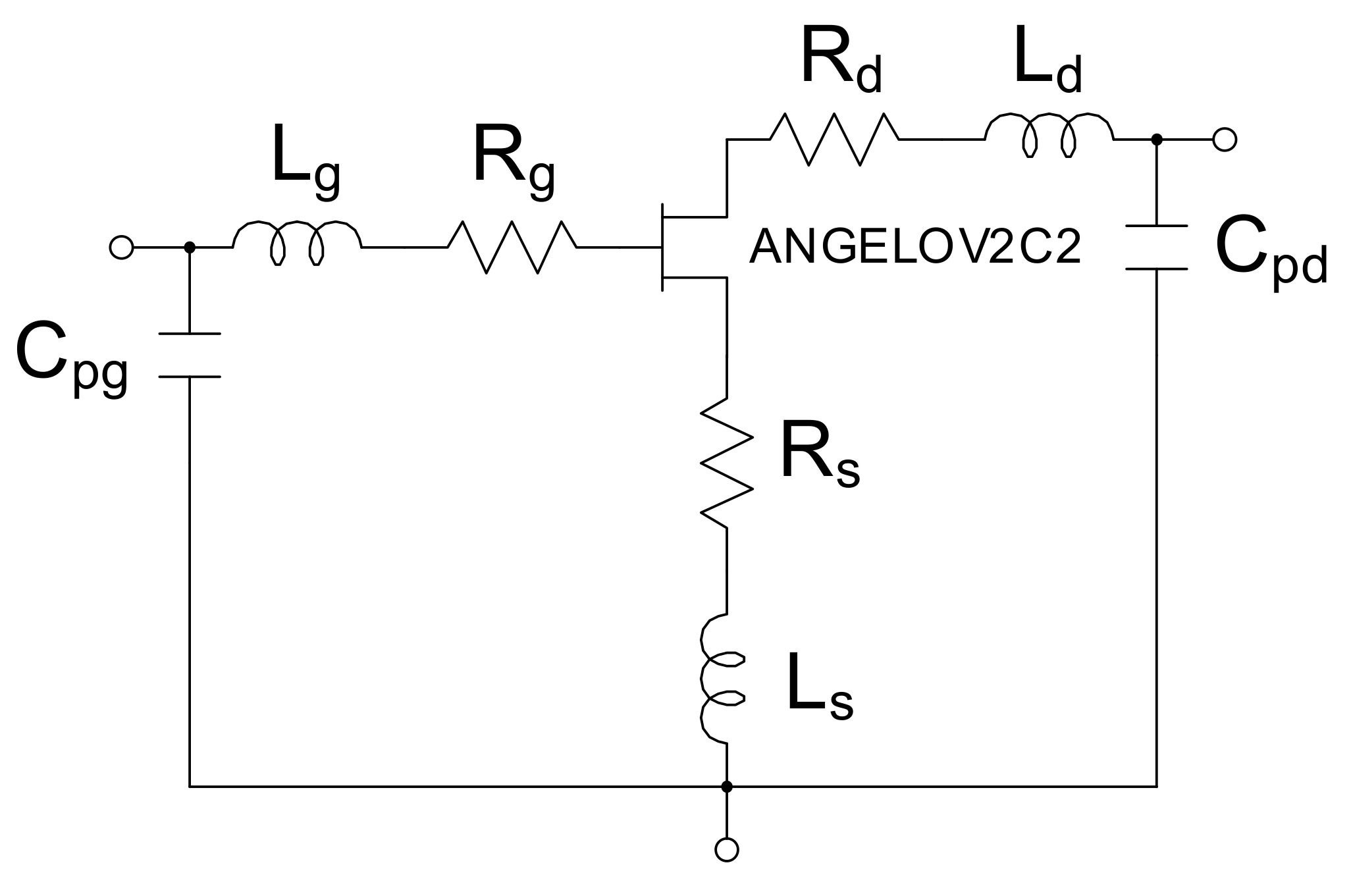
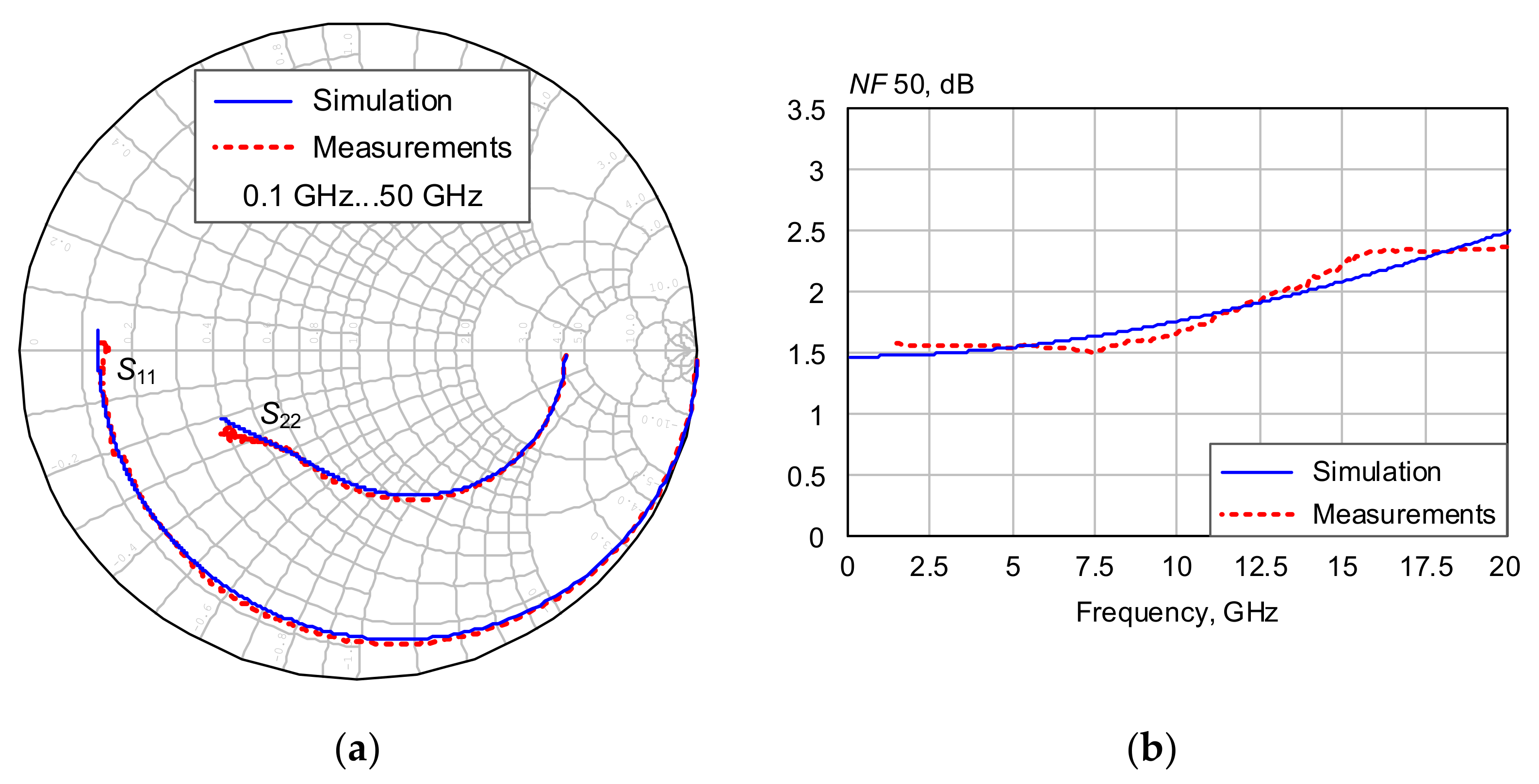
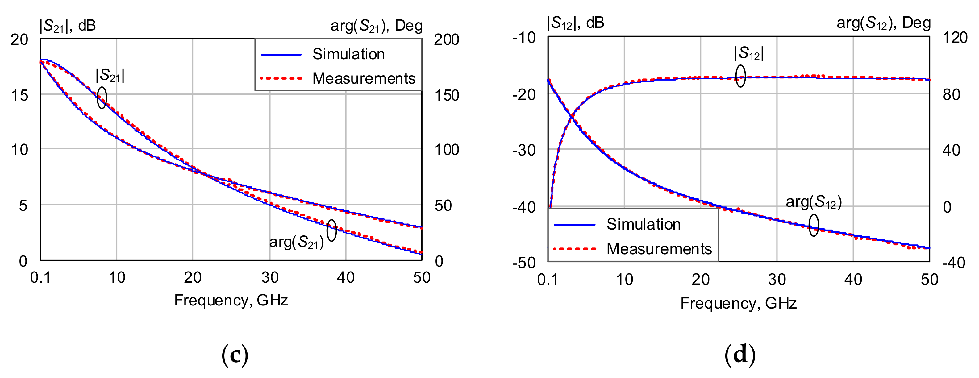
- IV-curves;
- S-parameters;
- Noise-figure.
- De-embedding;
- Smoothing.
- S-parameter measurement results of test structures of individual elements;
- S-parameter measurement results of network fragments for matching and correction (consist of several passive elements);
- Electromagnetic analysis results;
- Topological design rules.
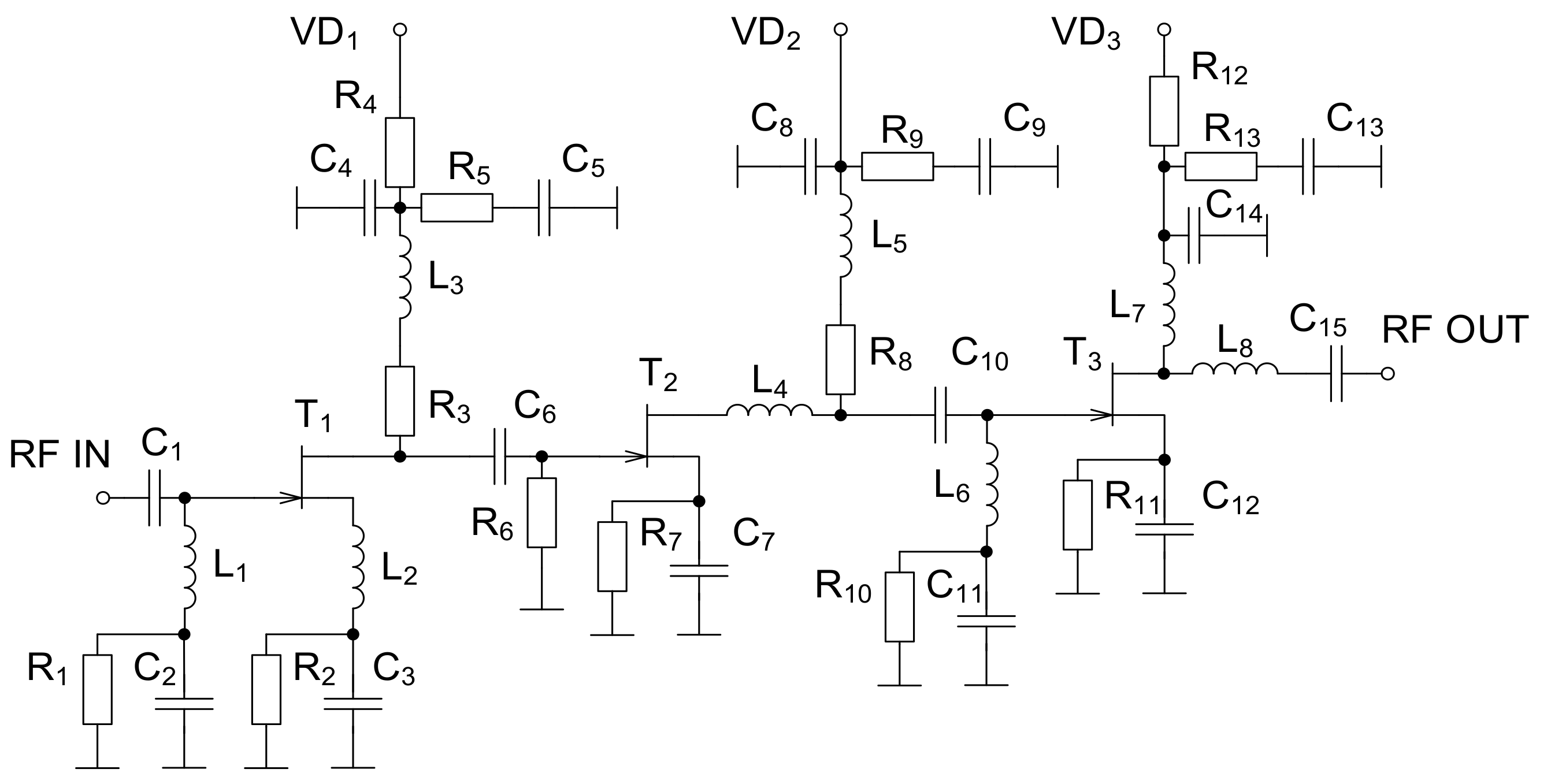
- Single-stage LNA;
- Two-stage LNA;
- Three-stage LNA.
4. Discussion
- Buffer amplifiers;
- Switches;
- Attenuators;
- Phase shifters;
- Frequency converters;
- Power limiters.
Author Contributions
Funding
Acknowledgments
Conflicts of Interest
Abbreviations
| pHEMT | Pseudomorphic high-electron mobility transistor |
| PDK | Process design kit |
| MMIC | Monolithic microwave integrated circuit |
| EDA | Electronic design automation |
| RF | Radio frequency |
| MIM | Metal insulator metal |
| PCM | Process control monitor |
| LNA | Low-noise amplifiers |
References
- Bahl, I.J. Fundamentals of RF and Microwave Transistor Amplifiers; John Wiley & Sons, Inc.: Hoboken, NJ, USA, 2008; pp. 419–452. [Google Scholar] [CrossRef]
- Colantonio, P.; Giannini, F.; Limiti, E. High Efficiency RF and Microwave Solid State Power Amplifiers; John Wiley & Sons, Ltd.: Chichester, UK, 2009; pp. 49–83. [Google Scholar] [CrossRef]
- Robertson, I.D.; Lucyszyn, S. RFIC and MMIC Design and Technology; The Institution of Electrical Engineers: London, UK, 2001; pp. 125–181. [Google Scholar]
- Saha, S.K. Compact Models for Integrated Circuit Design, 1st ed.; CRC Press: Boca Raton, FL, USA, 2016; 545p. [Google Scholar] [CrossRef] [Green Version]
- Kompa, G. Parameter Extraction and Complex Nonlinear Transistor Models; Artech House: Norwood, MA, USA, 2019; 610p. [Google Scholar]
- Aaen, P.; Plá, J.A.; Wood, J. Modeling and Characterization of RF and Microwave Power FETs; Cambridge University Press: New York, NY, USA, 2007; 362p. [Google Scholar] [CrossRef] [Green Version]
- Bahl, I.J. Lumped Elements for RF and Microwave Circuits; Artech House: Norwood, MA, USA, 2003; 488p. [Google Scholar]
- Wolff, I. Coplanar Microwave Integrated Circuits; John Wiley & Sons, Inc.: Hoboken, NJ, USA, 2006; 545p. [Google Scholar] [CrossRef]
- Yoshitomi, S. Combination of Transistors’ compact model and Big Data For successful Smart Factory. In Proceedings of the 2020 International Symposium on Devices, Circuits and Systems (ISDCS), Howrah, India, 4–6 March 2020; pp. 1–6. [Google Scholar] [CrossRef]
- Koolen, M.; Geelen, J.A.M.; Versleijen, M. An improved de-embedding technique for on-wafer high-frequency characterization. In Proceedings of the 1991 Bipolar Circuits and Technology Meeting, Minneapolis, MN, USA, 9–10 September 1991; pp. 188–191. [Google Scholar] [CrossRef]
- Kim, J.Y.; Choi, M.K.; Lee, S. A “Thru-Short-Open” de-embedding method for accurate on-wafer RF measurements of nano-scale MOSFETs. J. Semicond. Technol. Sci. 2012, 12, 53–58. [Google Scholar] [CrossRef] [Green Version]
- Wu, Y.; Liu, J.; Zhao, C.; Xu, Y.; Yin, W.; Kang, K. An improved ultrawideband open-short de-embedding method applied up to 220 GHz. IEEE Trans. Compon. Packag. Manuf. Technol. 2017, 8, 53–58. [Google Scholar] [CrossRef]
- Ding, W.; Ding, P.; Su, Y.; Zhou, J.; Yang, F.; Hu, J.; Jin, Z. A de-embedding method with matrix rectification and influences of residual errors on model parameters extraction of InP HEMTs. Int. J. RF Microw. Comput. Aided Eng. 2020, 30, e22218. [Google Scholar] [CrossRef]
- Dambrine, G.; Cappy, A.; Heliodore, F.; Playez, E. A new method for determining the FET small-signal equivalent circuit. IEEE Trans. Microw. Theory Tech. 1988, 36, 1151–1159. [Google Scholar] [CrossRef]
- Berroth, M.; Bosch, R. Broad-band determination of the FET small-signal equivalent circuit. IEEE Trans. Microw. Theory Tech. 1990, 38, 891–895. [Google Scholar] [CrossRef] [Green Version]
- Crupi, G.; Schreurs, D.M.M.-P.; Caddemi, A. On the small signal modeling of advanced microwave FETs: A comparative study. Int. J. RF Microw. Comput. Aided Eng. 2008, 18, 417–425. [Google Scholar] [CrossRef]
- Tayrani, R.; Gerber, J.E.; Daniel, T.; Pengelly, R.S.; Rohde, U.L. A new and reliable direct parasitic extraction method for MESFETs and HEMTs. In Proceedings of the 23rd European Microwave Conference 1993, Madrid, Spain, 6–10 September 1993; pp. 451–453. [Google Scholar] [CrossRef]
- Costa, D.; Liu, W.U.; Harris, J.S. Direct extraction of the AlGaAs/GaAs heterojunction bipolar transistor small-signal equivalent circuit. IEEE Trans. Electron. Devices 1991, 38, 2018–2024. [Google Scholar] [CrossRef]
- Nalli, A.; Raffo, A.; Crupi, G.; D'Angelo, S.; Resca, D.; Scappaviva, F.; Salvo, G.; Caddemi, A.; Vannini, G. GaN HEMT Noise Model Based on Electromagnetic Simulations. IEEE Trans. Microw. Theory Tech. 2015, 63, 2498–2508. [Google Scholar] [CrossRef]
- Caddemi, A.; Crupi, G. On the noise measurements and modeling for on wafer HEMTs up to 26. 5 GHz. Microw. Opt. Technol. Lett. 2010, 52, 1799–1803. [Google Scholar] [CrossRef]
- Pospieszalski, M.W. Modeling of noise parameters of MESFETs and MODFETs and their frequency and temperature dependence. IEEE Trans. Microw. Theory Tech. 1989, 37, 1340–1350. [Google Scholar] [CrossRef]
- Gao, J.; Law, C.L.; Wang, H.; Aditya, S.; Boeck, G. A new method for pHEMT noise-parameter determination based on 50-Ω noise measurement system. IEEE Trans. Microw. Theory Tech. 2003, 51, 2079–2089. [Google Scholar] [CrossRef]
- Popov, A.A.; Bilevich, D.V.; Salnikov, A.S.; Dobush, I.M.; Goryainov, A.E.; Kalentyev, A.A. Automatic large-signal GaAs HEMT modeling for power amplifier design. AEU Int. J. Electron. Commun. 2019, 100, 138–143. [Google Scholar] [CrossRef]
- Popov, A.A.; Bilevich, D.V.; Salnikov, A.S.; Dobush, I.M.; Goryainov, A.E.; Kalentyev, A.A.; Metel, A.A. A Combined technique for amplifier oriented small-signal noise model extraction. Int. J. RF Microw. Comput. Aided Eng. 2020, 30, e22273. [Google Scholar] [CrossRef]
- Salnikov, A.S.; Goryainov, A.E.; Dobush, I.M.; Kalentyev, A.A. Approach to scalable modeling for planar inductor using em simulation and a few samples measurement. In Proceedings of the 2017 IEEE MTT-S International Conference NEMO 2017, Seville, Spain, 17–19 May 2017; pp. 55–57. [Google Scholar] [CrossRef]


| Parameter | Value | Units | Note |
|---|---|---|---|
| Drain current | 270 | mA/mm | At 0 gate-source voltage |
| Transconductance | 500 | mS/mm | |
| Drain breakdown voltage | 7 | V | |
| Gate threshold voltage | −0.8 | V | |
| Maximum generation frequency | 120 | GHz | For 4 × 50 μm |
| Minimum noise figure | 1.3 | dB | For 4 × 50 μm at 12 GHz |
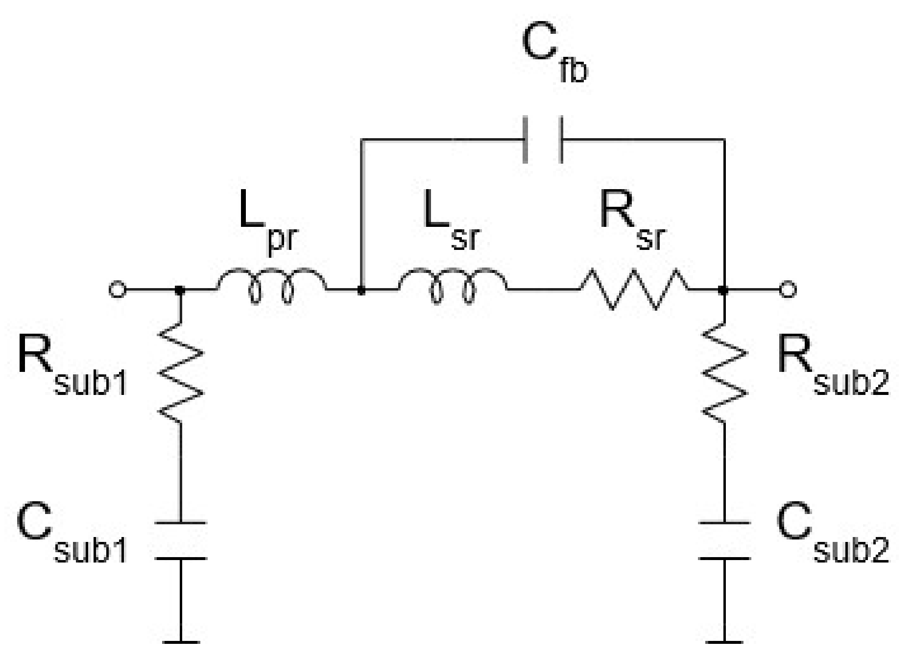
| Name | Lpr, nH | Lsr, nH | Rsr, ohm | Cfb, pF | Csub1, pF | Rsub1, ohm | Csub2, pF | Rsub2, ohm |
|---|---|---|---|---|---|---|---|---|
| L10101P5 | 0.2 | 0.269 | 0.8 | 0.0018 | 0.02016 | 5 | 0.02016 | 5 |
| L10102P5 | 0.316 | 0.8194 | 1.8 | 0.00228 | 0.03531 | 7.5 | 0.02931 | 7.5 |
| L10103P5 | 0.41 | 1.773 | 2.8 | 0.002 | 0.05 | 9 | 0.0388 | 7 |
| L10104P5 | 0.71 | 3.065 | 4 | 0.002 | 0.0632 | 9 | 0.047 | 9 |
| L10105P5 | 0.75 | 5 | 6 | 0.0015 | 0.07456 | 14 | 0.05536 | 10 |
| L10106P5 | 0.75 | 7.5 | 6.4 | 0.002 | 0.0917 | 12 | 0.068 | 11 |
| L10107P5 | 0.79 | 10.4 | 8.14 | 0.0022 | 0.1176 | 12 | 0.08558 | 12 |
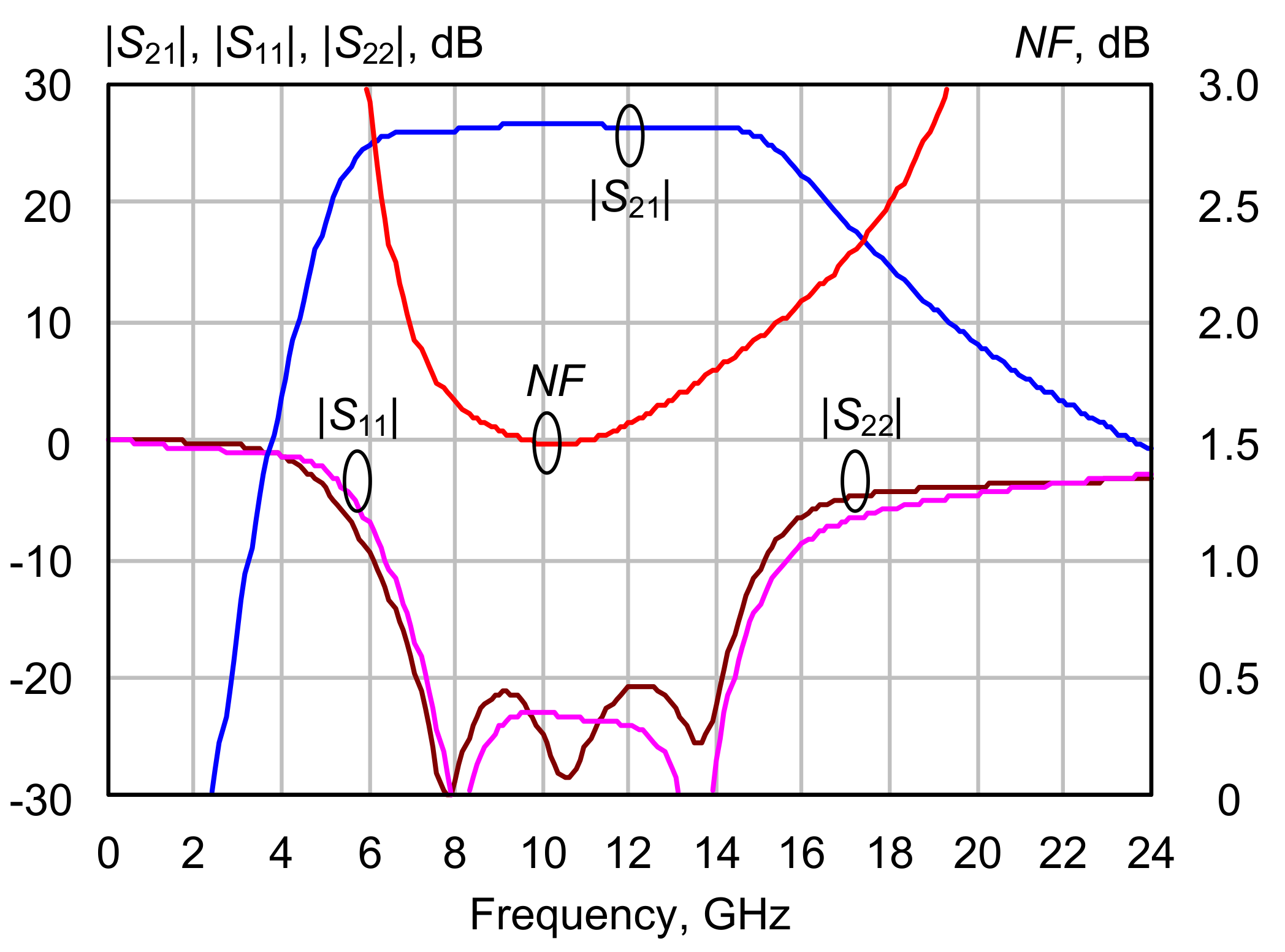
| Parameter | Simulated Value | Units |
|---|---|---|
| Frequency range | 8–12 | GHz |
| Small-signal gain, min | 26 | dB |
| Input and output reflection coefficient, max | −20 | dB |
| Noise figure, max | 1.7 | dB |
| Output power at 1 dB compression point, min | 13 | dBm |
| Supply voltage | 5 | VDC |
| DC current for supply bus | 85 | mA |
| Die size | 1.2 × 2.2 | mm2 |
Publisher’s Note: MDPI stays neutral with regard to jurisdictional claims in published maps and institutional affiliations. |
© 2021 by the authors. Licensee MDPI, Basel, Switzerland. This article is an open access article distributed under the terms and conditions of the Creative Commons Attribution (CC BY) license (https://creativecommons.org/licenses/by/4.0/).
Share and Cite
Dobush, I.M.; Vasil’evskii, I.S.; Zykov, D.D.; Bragin, D.S.; Salnikov, A.S.; Popov, A.A.; Gorelov, A.A.; Kargin, N.I. Development of a 0.15 μm GaAs pHEMT Process Design Kit for Low-Noise Applications. Electronics 2021, 10, 2775. https://doi.org/10.3390/electronics10222775
Dobush IM, Vasil’evskii IS, Zykov DD, Bragin DS, Salnikov AS, Popov AA, Gorelov AA, Kargin NI. Development of a 0.15 μm GaAs pHEMT Process Design Kit for Low-Noise Applications. Electronics. 2021; 10(22):2775. https://doi.org/10.3390/electronics10222775
Chicago/Turabian StyleDobush, Igor M., Ivan S. Vasil’evskii, Dmitry D. Zykov, Dmitry S. Bragin, Andrei S. Salnikov, Artem A. Popov, Andrey A. Gorelov, and Nikolay I. Kargin. 2021. "Development of a 0.15 μm GaAs pHEMT Process Design Kit for Low-Noise Applications" Electronics 10, no. 22: 2775. https://doi.org/10.3390/electronics10222775
APA StyleDobush, I. M., Vasil’evskii, I. S., Zykov, D. D., Bragin, D. S., Salnikov, A. S., Popov, A. A., Gorelov, A. A., & Kargin, N. I. (2021). Development of a 0.15 μm GaAs pHEMT Process Design Kit for Low-Noise Applications. Electronics, 10(22), 2775. https://doi.org/10.3390/electronics10222775