Article

High Dynamic Range Photocurrent Sensory Circuit with a Multi-Transistor Background Light Cancellation Loop for Photoplethysmography Sensing

1
Electrical and Communication Engineering Department, College of Engineering, United Arab Emirates University, Al Ain P.O. Box 15551, United Arab Emirates
2
Department of Family Medicine, College of Medicine and Health Sciences, United Arab Emirates University, Al Ain P.O. Box 15551, United Arab Emirates
*
Author to whom correspondence should be addressed.
Electronics 2021, 10(22), 2769; https://doi.org/10.3390/electronics10222769
Submission received: 7 September 2021 / Revised: 26 September 2021 / Accepted: 27 September 2021 / Published: 12 November 2021
(This article belongs to the Section Circuit and Signal Processing)

Abstract

:
In this article, we present a new photocurrent sensory circuit with a three-transistor background light cancellation. We describe our innovative photocurrent sensor-based blood pressure measuring device using a resistor-based current-to-voltage converter with a background light cancellation (BLC) loop. The photocurrent sensor is implemented using 0.35 μm standard CMOS technology and has zero average power consumption. The post-layout simulation for the photocurrent sensor shows a 1.3 MΩ transimpedance gain, a referred input noise current of 11 pA, and can reject a DC photocurrent up to 200 μA. This high DC rejection has been achieved due to the newly proposed multi-transistor BLC loop integrated with the sensor.

1. Introduction

Optical sensing and its acquisition circuits are gaining great interest, particularly in biomedical applications [1]. In current clinical practice, photoplethysmography (PPG)-based monitoring devices allow physicians to monitor heart rate, oxygen saturation level, and blood pressure without the need for invasive procedures [1,2]. This PPG sensing technique has helped in reducing costs and speeding up the diagnostic process [3,4,5]. It has assisted healthcare providers with continuous measurements to deliver treatments based upon more specific diagnoses and real-time continuous monitoring [6,7,8].
PPG sensors utilize a photodiode to convert the received optical power from human tissue into a photocurrent. The weak photocurrent is then converted into a stronger voltage output via the transimpedance amplifier (TIA) stage. The state-of-the-art TIA topologies that have been studied and presented in the literature try to optimize power consumptions, sensitivities, and bandwidths depending on the usage of different applications [9].
Despite the advances made in the PPG sensory circuits, several challenges remain, such as the large DC photocurrent cancellation and the associated high-pass filter effect [9]. The detected PPG signal perfusion index (PI) defined as the AC/DC ratio can vary from 0.1% to 3% [9]. A background light cancellation (BLC) loop is used to reject such a large DC component to prevent receiver saturation. To keep the PPG signal undistorted, the high-pass cut-off frequency involved within the BLC loop should be lower than 0.5 Hz. This implies that large BLC capacitor and resistor values should be implemented, which consume a large silicon area. For this reason, MOS pseudo-resistors [10], α-block, and Miller capacitance multipliers [11] have been used to achieve area-efficient solutions [9].
The proposed current sensor topology consists of a poly-resistor with three integrated Metal-Oxide Semiconductor Field-Effect transistors (MOSFET) for DC photocurrent cancellation (3T-BLC). The proposed novel 3T-BLC extends the PPG sensor dynamic range. The new proposed sensor with 3T-BLC performs better in terms of power, noise, and dynamic range than other state-of the-art topologies. Overall analysis, simulation, layout, and comparisons to state-of-the-art topologies are included for the proposed photocurrent sensory circuit.

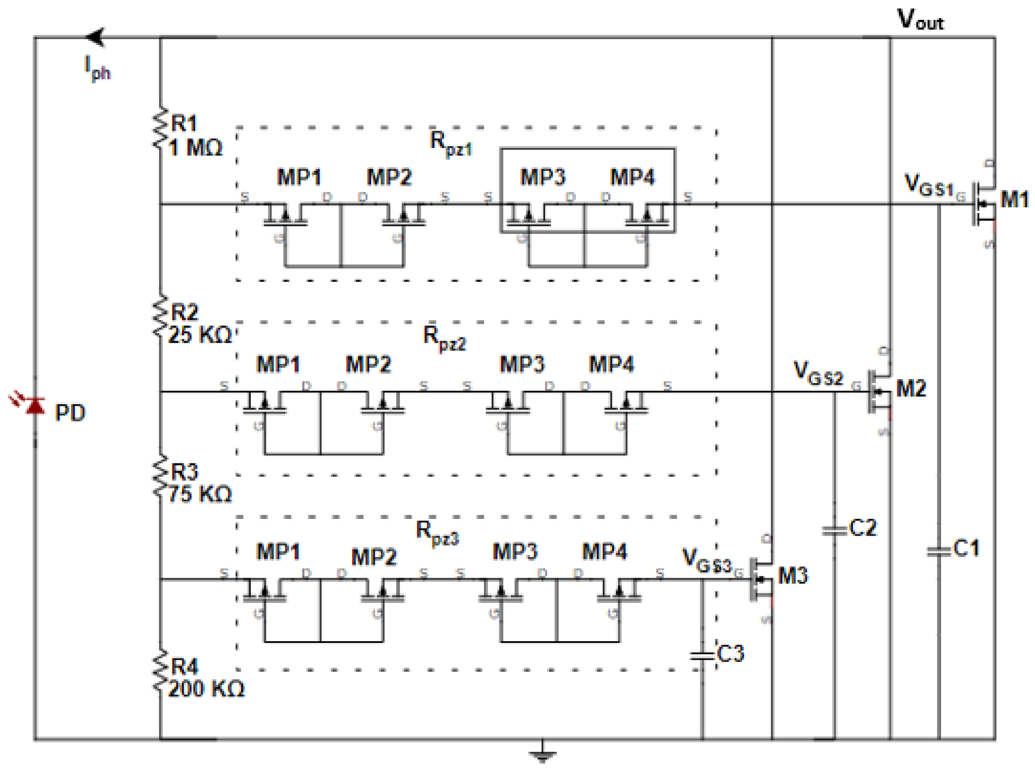
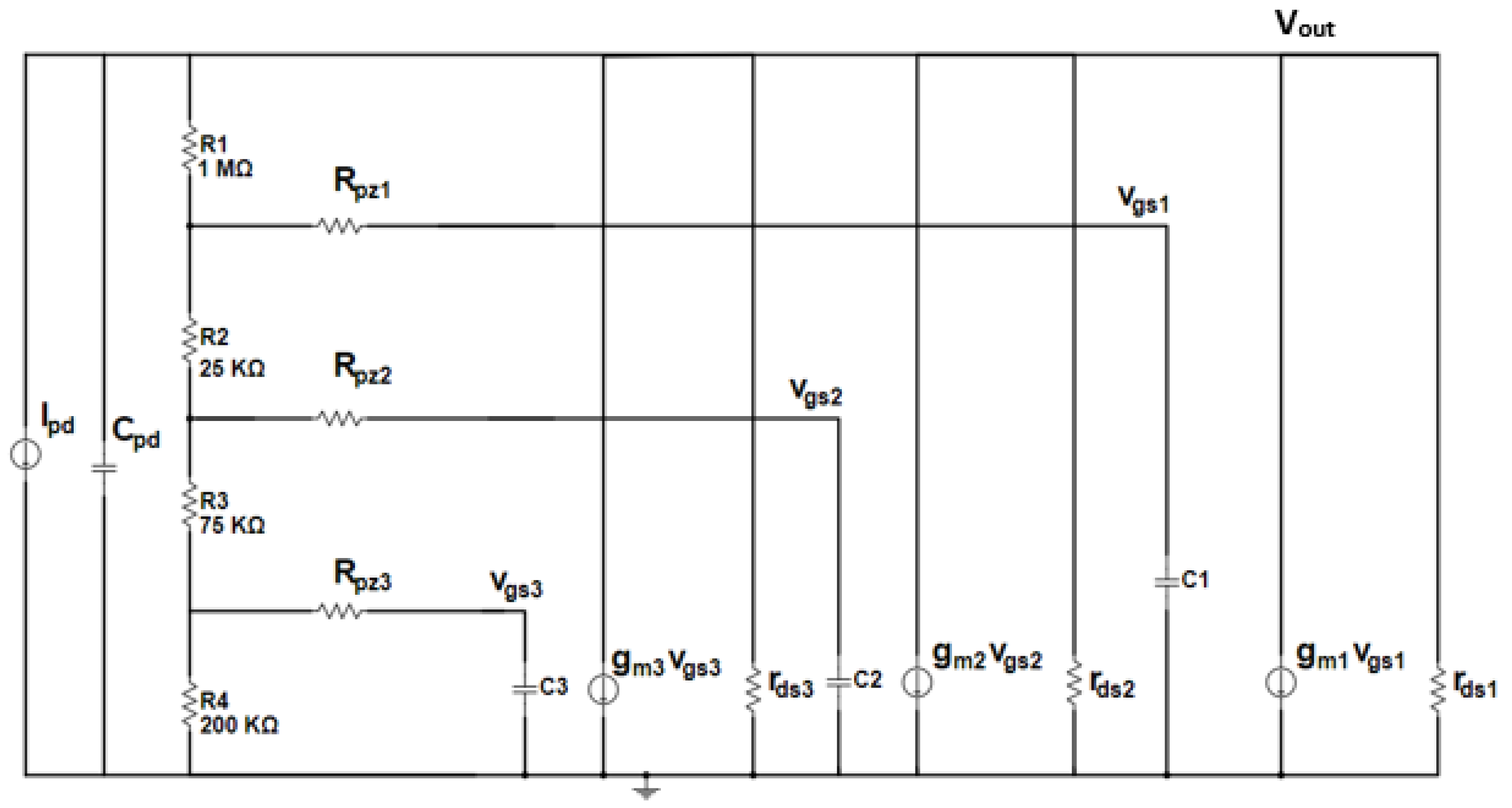
2. The Proposed 3T-BCL Photocurrent Sensory Circuit

The proposed photocurrent sensor in Figure 1 consists of four poly resistors (R1, R2, R3, and R4) that provide a high transimpedance gain of RT = R1 + R2 + R3 + R4. It uses four resistors to control the DC cancellation, as it ensures that the three MOSFETs turn on one at a time as the input photocurrent increases. The pseudo-resistors Rpz1,2,3 and capacitors C1,2,3 form a low pass filter (LPF) that extracts the DC component from the input PPG photocurrent signal. The pseudo-resistor can reach hundreds of Giga Ohms and a small capacitor can be used for the LPF. All MOSFETs are OFF at low input photocurrents. As the input photocurrent Iph increases, the voltage drop, Iph ∙ (R2 + R3 + R4), increases. The DC voltage after the LPF, VGS1 = Iph ∙ (R2 + R3 + R4), is large enough to turn the transistor M1 ON, and a DC current that is subtracted from Iph flows solely through M1. This is to ensure that the input-referred noise is low at small photocurrent levels as all other transistors are OFF and have no noise contribution. It is important to note that the voltage drops across the resistors VGS3 = Iph. R4 and VGS2 = Iph∙(R4 + R3) are smaller than the threshold voltage at small Iph. Therefore, after the photocurrent increases and reaches a certain value, the voltage drop VGS2 becomes enough to turn M2 ON. At higher photocurrents, VGS3 is large enough to turn M3 ON. This process of switching the transistors one at a time ensures a high-input dynamic range at a low-input noise current.
From the small-signal model in Figure 2, the transimpedance gain can be approximated by the following expression:
H s r ds R 1 + R 2 + R 3 + R 4 C 1 R z S + 1 C pd C 1 R z r ds R 1 S 2 + C pd r ds R 1 + C 1 R z R 1 + C 1 R z r ds S + R 1 + 2 r ds G m R 2 + R 3 + R 4
This approximated transfer function is valid considering that Rz >> R1 >> R2, R3, R4, where Gm = gm1 + gm2 + gm3, rds = rds1//rds2//rds3, and C1 = C2 = C3.
Moreover, the transfer function of the transimpedance amplifier has two poles, and the bandwidth can be approximated by the dominant pole as:
BW = R 1 + r ds 2   π   r ds   C PD   R 1
where rds is the equivalent drain to source resistance of the transistors, and CPD is the photodiode capacitance. The drain to source resistance rds is inversely proportional to the gate voltages of the transistors. Therefore, as the photocurrent increases, the bandwidth increases because of its dependence on rds. The designed bandwidth was chosen to be 6.1 kHz because the duty cycle control of the transmitter operates within the kHz range, and the transimpedance amplifier was designed with the intention of being used with duty cycle control PPG sensors. The midband gain (maximum gain at S = 0) of the current sensor is given as:
R T r ds R 1 + R 2 + R 3 + R 4 R 1 + 2 g m r ds R 2 + R 3 + R 4
I n , in = 4 KT 1 R 1 + R 2 + R 3 + R 4 + 1 r ds 1   R 1 + r ds 4   r ds   C PD   R 1
where 4KT is 26 mV at room temperature, CPD is the photodiode capacitance and is selected to be 20 pF for a large-area photodiode, rds can vary from hundreds of kilo ohms at a low input photocurrent to tens of ohms at a high input photocurrent. The calculated noise current is 12.5 pA compared to the 11 pA simulated noise at an input photocurrent less than 500 nA.

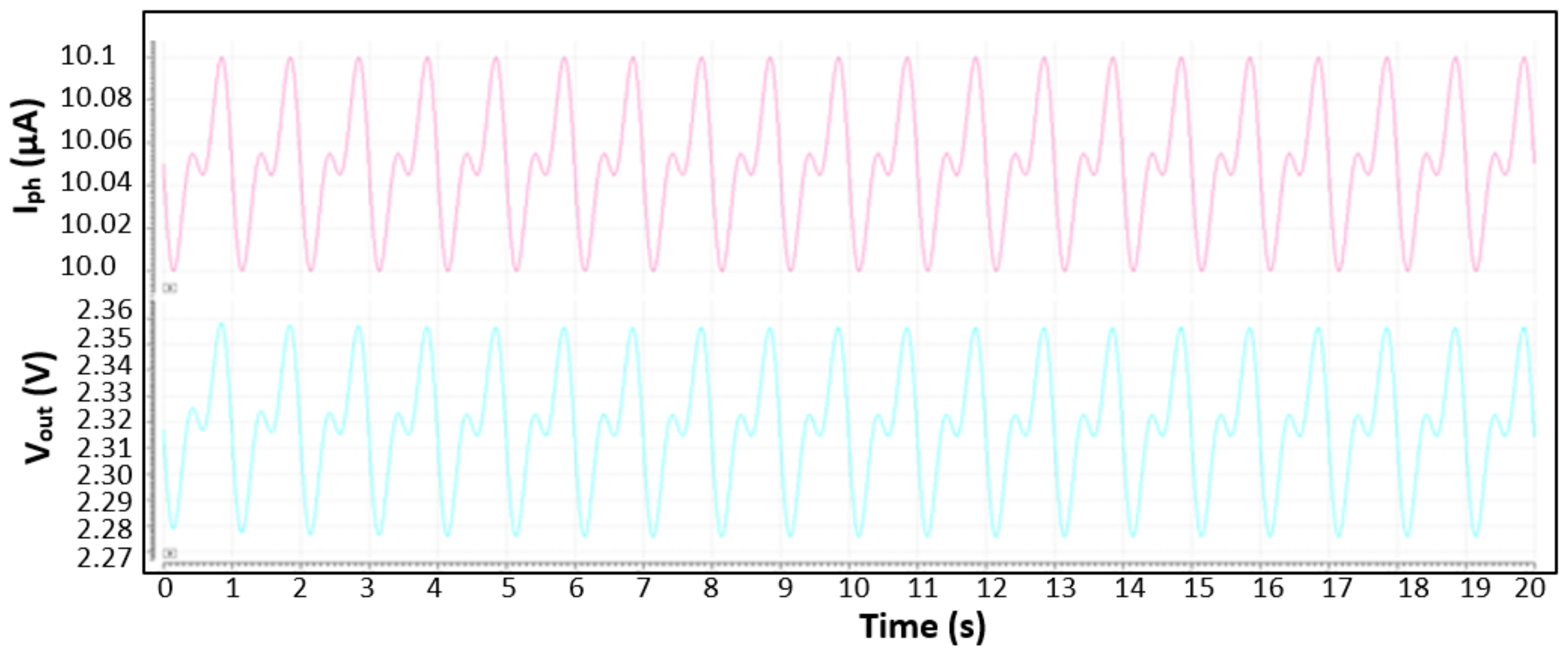
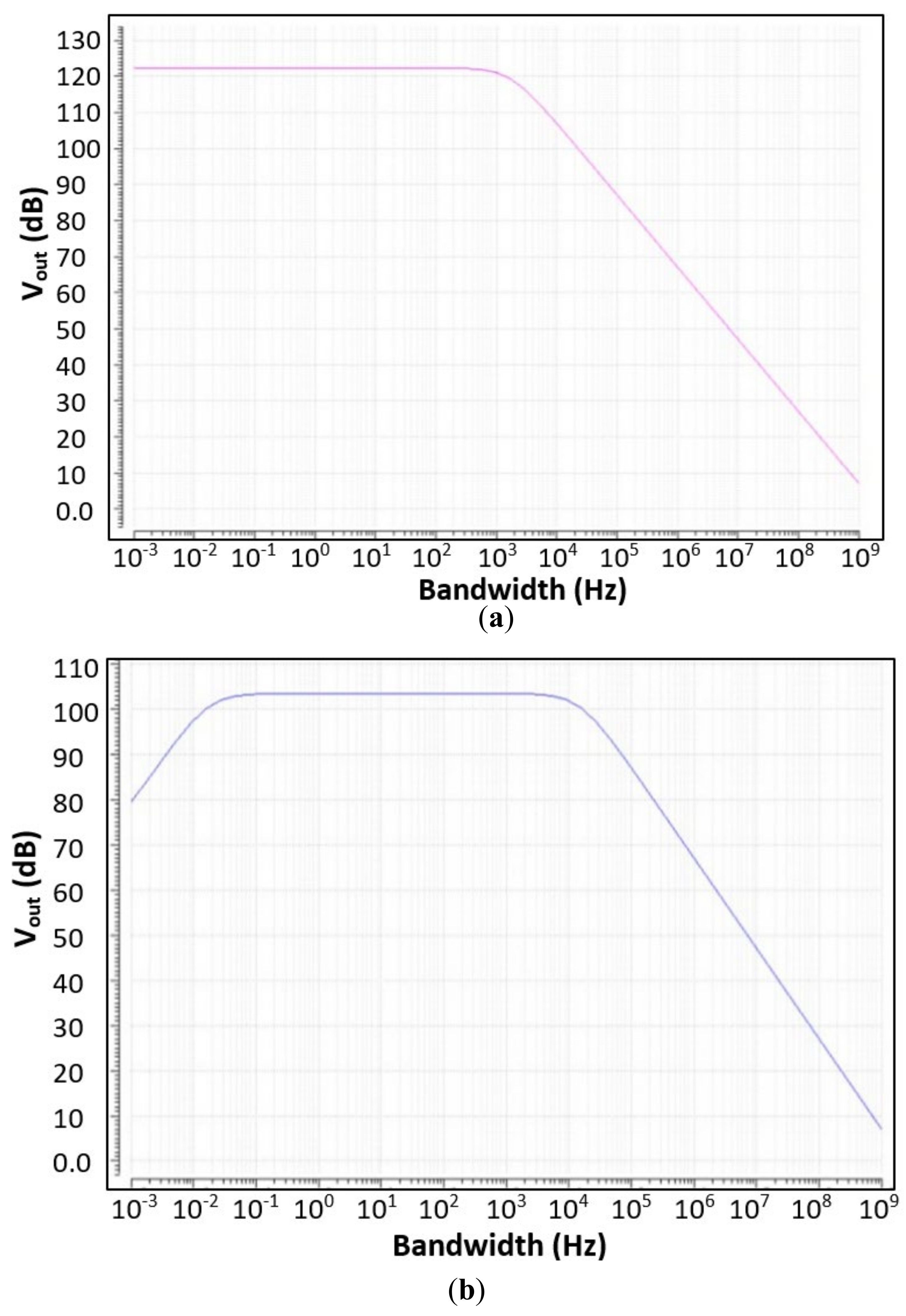
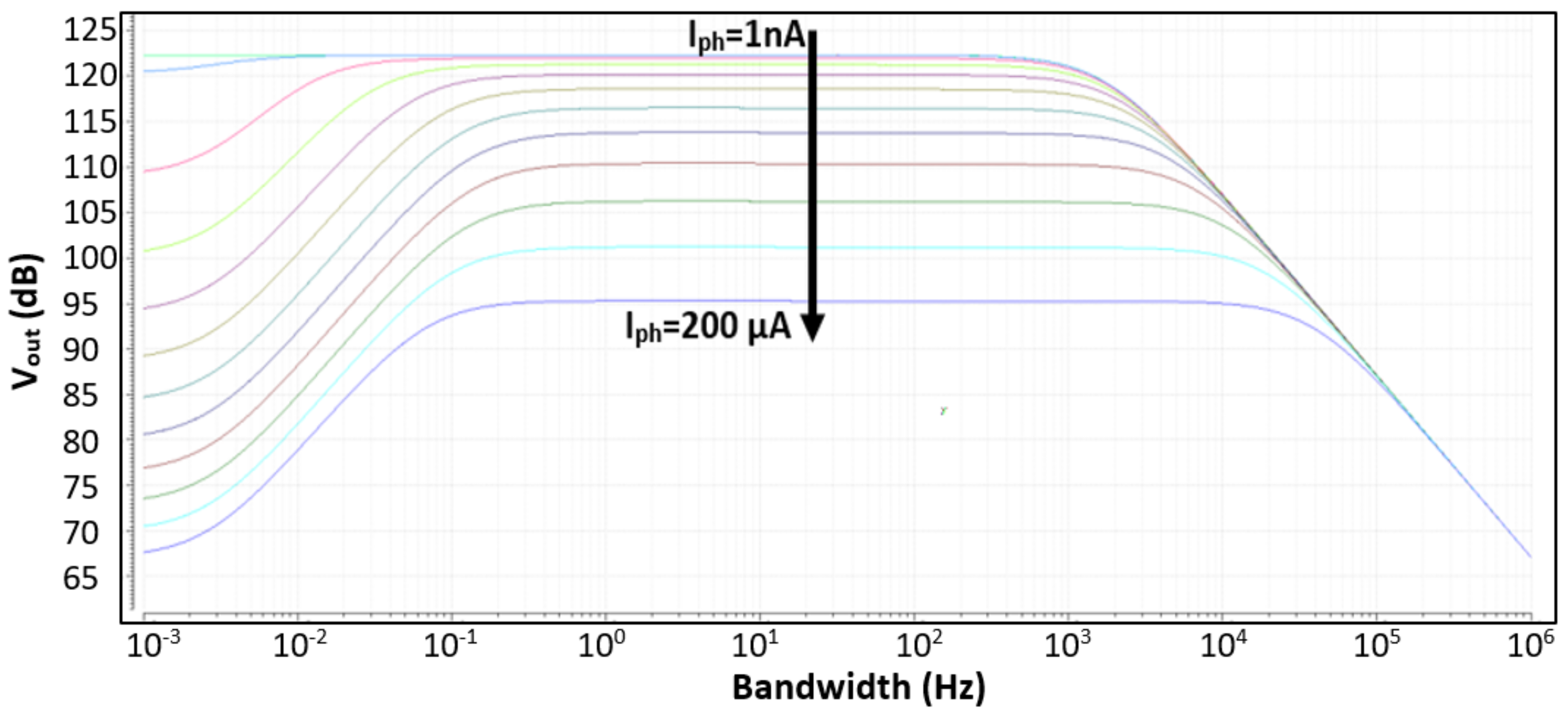
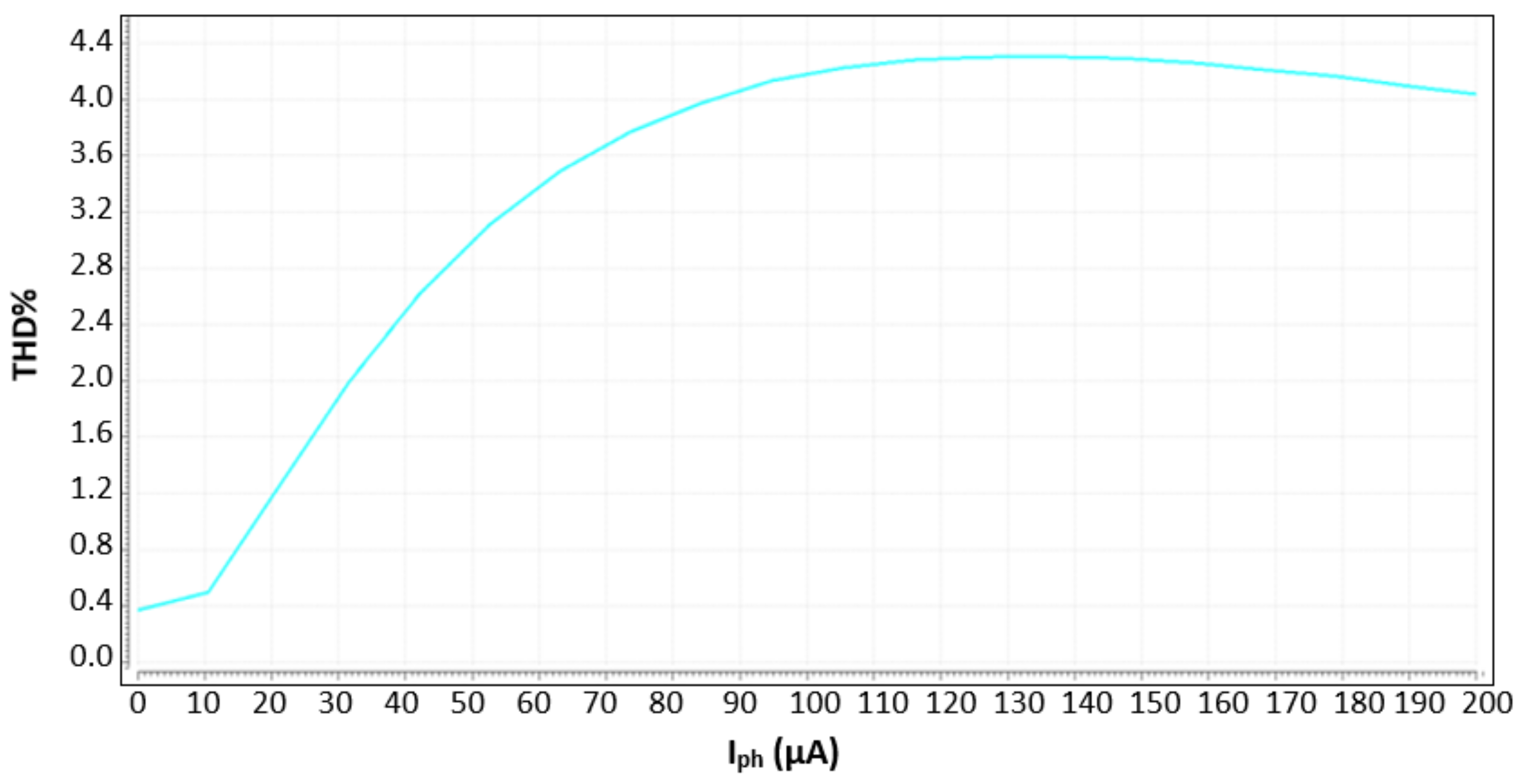
3. Photocurrent Sensory Circuit Simulation

In this section, the simulation results obtained for the proposed photocurrent sensory circuit are introduced. Furthermore, comparisons between the simulation results, the model obtained from the previous section, and the post-layout simulation results will be presented in this section. The simulation parameters are listed in Table 1.
Transient analysis is performed (Figure 3) for the transimpedance amplifier at a 10 μA photocurrent. The input signal in this simulation is a waveform with an AC amplitude of 0.1 μA. The output maintains the input’s waveform while amplifying the amplitude by 118 dBΩ. The gain shows that there are no significant differences between the model and the simulated data.
For the frequency response in Figure 4, the frequency range is set from 1 MHz to 1 GHz. The input signal in this simulation is a sinusoidal waveform with an amplitude of 1 V. Figure 4a shows the frequency response at a photocurrent of 200 μA. It is clear that in this case, the amplitude of the output signal is attenuated at frequencies lower than 0.1 Hz. This is due to a second pole occurring at high photocurrents. However, its effect is nullified at small photocurrents (Figure 4b) because of the appearance of a zero in the transimpedance transfer function, which is given by
ω z = 1 C 1 R pz
A value of 15 pF is chosen for C1 to ensure that the pole only attenuates the gain at frequencies lower than 0.4 Hz.
Figure 5 shows the frequency response of the 3T-BCL sensor for different input currents up to 200 μA. As the input current increases, the gain decreases, which is consistent with the gain expression in Equation (3). The frequency response has a bandpass filter shape at high photocurrents. The bandwidth increases by increasing the photocurrent (rds decreases with a higher current).
Table 2 shows the simulation results for the transimpedance amplifier, as well as mathematical model results for the gain and bandwidth. The simulation results obtained match well with the model simulation results. As expected, a considerable increase in the bandwidth is observed as the photocurrent became greater due to decreasing rds. The calculated bandwidth and gain using our model match well with the simulated gain and bandwidth results for different photocurrents.

4. Transimpedance Amplifier Layout and Literature Comparison

The layout was designed using Cadence Virtuoso’s Analog Design Environment tool using AMS 0.35 μm CMOS technology. This section presents the post-layout simulation results using AMS 0.35 μm CMOS technology. This is a mature technology with an accurate PDK. From our experience, there is a small deviation from the exponential results of a fabricated chip compared to the post-layout simulation, especially at this low-frequency range. The final layout obtained is shown in Figure 6. The post-layout simulation results are shown in Table 3.
The proposed 3T-BCL photocurrent sensor introduces many advantages over the traditional single transistor BCL transimpedance amplifier. The proposed topology can operate within larger photocurrent ranges (200 μA) without saturation. Table 4 shows the comparison of the single transistor to the proposed 3T-BCL topology. The single transistor topology reaches VDD = 3.3 V at a photocurrent of less than 100 μA. Despite increasing the traditional single transistor BCL width (W = 50 μm), the TIA is still saturated at a lower photocurrent than the proposed 3T-BCL TIA.
A single transistor with a larger width (W = 50 μm) can extend the dynamic range up to 150 μA without crossing the 3.3 V threshold. However, it still falls short of the proposed amplifier’s noise performance. This is because the proposed amplifier has three transistors, contributing smaller noise than the wider single transistor working early at weaker photocurrent values. To study the linearity, the total harmonic distortion (THD) was simulated and plotted in Figure 7 for different input photocurrents up to 200 μA. The worst THD is 4.3% at 130 μA.
Figure 8 depicts the influence of process variation on the proposed 3T-BCL topology. The transimpedance gain and bandwidth are calculated for 300 runs. The mean value of the transimpedance gain is 122.27 dBΩ with a standard deviation of 0.855 dBΩ, and the bandwidth mean value is 6.2 KHz with a standard deviation of 642 Hz.
Table 5 shows the comparison of this work with recently published works. Despite the TIA in [12] using the advanced 65 nm technology, it could only reach a 4 μA maximum photocurrent with high input noise of 68 pA, as it was targeting low power consumption with a 0.5 V power supply, and high bandwidth was used. The work in [13] implemented in 55 nm technology reached a 75 μA photocurrent using a current digital-to-analog converter (IDAC) to cancel the DC component. An ADC and FIR digital filter are required for DC cancellation. Moreover, the additional 1/f noise of the IDAC can be cancelled by correlated double sampling, and the input noise can reach 28 pA. The PPG sensor in [14] has the highest gain of 12.5 MΩ and can reach 24 μA using an Analog BLC loop, but the noise is still as high as 41.3 pA. The results in Table 5 show that our proposed 3T-BLC photocurrent sensor topology has the lowest input referred noise. Moreover, it can operate for an input photocurrent range of up to 200 μA.

5. Conclusions

A new photocurrent sensory circuit with a three-transistor background light cancellation is presented. The proposed design succeeded in reaching a higher dynamic range and better noise performance in comparison to other recently published works. The input current can be varied up to 200 μA, a range not available in other PPG-based transimpedance amplifiers. The simulation results suggest that the proposed topologies are suitable for long-term use in PPG-based sensors and in biomedical applications. The high dynamic range of this topology allows for capturing weak signals with high sensitivities, reaching higher accuracy even with large input DC components.

Author Contributions

Funding acquisition, M.A., F.A. and M.A.B.K. Methodology, M.A., O.H. Project administration, M.A., F.A. and M.A.B.K. Supervision, M.A. Visualization, O.H.; Writing—original draft, O.H.; Writing—review & editing, M.A., F.A. and M.A.B.K. All authors have read and agreed to the published version of the manuscript.

Funding

This work was supported by the United Arab Emirates University under grant G00003441.

Acknowledgments

This work was supported by the United Arab Emirates University under grant G00003441.

Conflicts of Interest

The authors declare no conflict of interest.

References

  1. Bielecki, Z.; Stacewicz, T.; Wojtas, J.; Mikolajczyk, J.; Szabra, D.; Prokopiuk, A. Selected Optoelectronic Sensors in Medical Applications. Opto-Electron. Rev. 2018, 26, 122–133. [Google Scholar] [CrossRef]
  2. Chen, Z.; Obaid, S.N.; Lu, L. Recent advances in organic optoelectronic devices for biomedical applications. Opt. Mater. Express 2019, 9, 3843–3856. [Google Scholar] [CrossRef]
  3. Castaneda, D.; Esparza, A.; Ghamari, M.; Soltanpur, C.; Nazeran, H. A Review on Wearable Photoplethysmography Sensors and Their Potential Future Applications in Health Care. Int. J. Biosens. Bioelectron. 2018, 4, 195–202. [Google Scholar] [PubMed] [Green Version]
  4. Shin, H.; Min, S.D. Feasibility study for the non-invasive blood pressure estimation based on ppg morphology: Normotensive subject study. Biomed. Eng. Online 2017, 16, 10. [Google Scholar] [CrossRef] [PubMed] [Green Version]
  5. Elgendi, M.; Fletcher, R.; Liang, Y.; Howard, N.; Lovell, N.H.; Abbott, D.; Lim, K.; Ward, R. The use of photoplethysmography for assessing hypertension. NPJ Digit. Med. 2019, 2, 60. [Google Scholar] [CrossRef] [PubMed] [Green Version]
  6. Ahmed, A.N.R.; Barbé, K.; Ottevaere, H. Photonic Sensor Design Evaluation for Measuring the Photoplethysmogram. In Proceedings of the 2016 IEEE International Instrumentation and Measurement Technology Conference Proceedings, Taipei, Taiwan, 23–26 May 2016; pp. 1–6. [Google Scholar]
  7. Hosanee, M.; Chan, G.; Welykholowa, K.; Cooper, R.; Kyriacou, P.A.; Zheng, D.; Allen, J.; Abbott, D.; Menon, C.; Lovell, N.H.; et al. Cuffless Single-Site Photoplethysmography for Blood Pressure Monitoring. J. Clin. Med. 2020, 9, 723. [Google Scholar] [CrossRef] [PubMed] [Green Version]
  8. Laulkar, R.; Daimiwal, N. Acquisition of PPG Signal for Diagnosis of Parameters Related to Heart. In Proceedings of the 2012 1st International Symposium on Physics and Technology of Sensors (ISPTS-1), Pune, India, 7–10 March 2012; pp. 274–277. [Google Scholar]
  9. Wang, G.; Atef, M.; Lian, Y. Towards a Continuous Non-Invasive Cuffless Blood Pressure Monitoring System Using PPG: Systems and Circuits Review. IEEE Circuits Syst. Mag. 2018, 18, 6–26. [Google Scholar] [CrossRef]
  10. Lin, B.; Atef, M.; Wang, G. 14.85 µW Analog Front-End for Photoplethysmography Acquisition with 142-dBΩ Gain and 64.2-pArms Noise. Sensors 2019, 19, 512. [Google Scholar] [CrossRef] [PubMed] [Green Version]
  11. Li, Y.; Wong, A.; Zhang, Y.-T. Fully-integrated transimpedance amplifier for photoplethysmographic signal processing with two-stage Miller capacitance multiplier. Electron. Lett. 2010, 46, 745–746. [Google Scholar] [CrossRef]
  12. Saadeh, W.; Aslam, S.Z.; Hina, A.; Asghar, F. A 0.5V PPG-based Heart Rate and Variability Detection System. In Proceedings of the 2018 IEEE Biomedical Circuits and Systems Conference (BioCAS2018), Cleveland, OH, USA, 17–19 October 2018; pp. 1–4. [Google Scholar]
  13. Song, S.; Konijnenburg, M.; Van Wegberg, R.; Xu, J.; Ha, H.; Sijbers, W.; Stanzione, S.; Biswas, D.; Breeschoten, A.; Vis, P.; et al. A 769 μW Battery-Powered Single-Chip SoC With BLE for Multi-Modal Vital Sign Monitoring Health Patches. IEEE Trans. Biomed. Circuits Syst. 2019, 13, 1506–1517. [Google Scholar] [CrossRef] [PubMed]
  14. Binghui, L.; Zhouchen, M.; Atef, M.; Ying, L.; Wang, G. Low-Power High-Sensitivity Photoplethysmography Sensor for Wearable Health Monitoring System. IEEE Sens. J. 2021, 21, 16141–16151. [Google Scholar]
Figure 1. The proposed photocurrent sensory circuit with 3T-BCL.
Electronics 10 02769 g001
Figure 2. The small signal model of the photocurrent sensory circuit.
Electronics 10 02769 g002
Figure 3. The input PPG photocurrent (10 μA) and the output voltage.
Electronics 10 02769 g003
Figure 4. Frequency response at (a) Iph = 1 nA, (b) Iph = 200 μA.
Electronics 10 02769 g004
Figure 5. Frequency response of the proposed photocurrent sensor for different input currents from 1nA up to 200 μA.
Electronics 10 02769 g005
Figure 6. The proposed photocurrent sensory circuit layout.
Electronics 10 02769 g006
Figure 7. The total harmonic distortion for different photocurrents.
Electronics 10 02769 g007
Figure 8. Monte-Carlo simulation for the proposed 3T-BCL topology; (a) gain, dB (b) bandwidth, KHz.
Electronics 10 02769 g008
Table 1. Simulation parameters.
R1R2R3R4CPDWM1, WM2, WM3C1, C2, C3
1 MΩ25 KΩ75 KΩ200 KΩ20 pF30 μm15 pF
Table 2. Calculated and simulated results for the gain and bandwidth.
IphSimulated GainCalculated GainSimulated BWCalculated BWSimulated Input Noise
1 μA122.3 dBΩ122.48 dBΩ7.36 KHz7.96 KHz15.4 pA
100 μA102.9 dBΩ105.3 dBΩ56.75 KHz57.4 KHz5.6 nA
Table 3. Post-layout simulation results for the gain and bandwidth.
IphPost Layout GainPost Layout Bandwidth
500 nA122.3 dBΩ6.134 KHz
1 μA122.3 dBΩ7.749 KHz
5 μA120.2 dBΩ7.645 KHz
10 μA118 dBΩ9.667 KHz
100 μA103.4 dBΩ51.64 KHz
Table 4. Comparison between the one transistor and 3T-BCL topologies.
IphInput Referred Thermal Noise Current
One Transistor (W = 30 μm)One Transistor (W = 50 μm)Three Transistors (W = 30 μm)
100 nA11.13 pA (130.6 mV)11.17 pA (130.6 mV)11 pA (130.6 mV)
500 nA11.15 pA (652.8 mV)11.17 pA (652.8 mV)11.16 pA (652.7 mV)
1 μA13.7 pA (1.294 V)15.1 pA (1.288 V)15.4 pA (1.285 V)
5 μA371 pA (2.23 V)311 pA (2.15 V)283.5 pA (2.15 V)
10 μA836.6 pA (2.41 V)692 pA (2.314 V)628.5 pA (2.316 V)
100 μA7.46 nA (3.203 V)6.34 nA (2.98 V)5.6 nA (2.94 V)
200 μA13 nA (3.6 V)11.5 nA (3.3 V)10.1 nA (3.2 V)
Table 5. Comparison with recently published research for PPG-based TIA.
Design[12][13][14]This Work
Technology65 nm55nm350 nm350 nm
TIA Gain1.8 MΩ1 MΩ12.5 MΩ1.3 MΩ
Bandwidth300 kHz8 kHz35 kHz6.17 kHz
Input Noise Current68 pA28 pA41.3 pA11 pA
Maximum photocurrent4 μA75 μA24 μA200 μA
Publisher’s Note: MDPI stays neutral with regard to jurisdictional claims in published maps and institutional affiliations.

