1. Introduction
The general broadband gain amplifier is widely used as the drive amplifier of a transmitter or a buffer amplifier in a receiver to provide a high linear dynamic range. Applications include mobile infrastructure, cable television (CATV), radar, satellite communication, point to point, and general-purpose wireless. In addition, with the recent evolution of communication systems such as 5 G (Sub-6 GHz) and Wi-Fi 6/6E, a broadband gain amplifier including additional frequency bands is strongly required [
1,
2]. For bands from the near DC to the 5 GHz band, gain amplifiers using various techniques have been reported [
1,
2,
3,
4,
5,
6,
7,
8,
9,
10,
11,
12,
13,
14,
15,
16,
17,
18,
19]. However, it is not easy to keep the S
21 flatness for a wide frequency band due to the difficulty to realize the matching circuit for varying impedance over frequency. Therefore, in a gain amplifier for mass-production, it is necessary to configure a matching circuit using different matching component values according to a specific frequency [
3,
4,
5].
For broadband amplifier designs, Darlington amplifiers with feedback have been widely used due to the advantage of allowing wideband impedance matching without additional circuitry [
6,
7,
8]. They have a structure that combines the output signals at the common drain of two transistors. Here, the parasitic capacitance of the transistors makes it difficult to have wide-band impedance matching characteristics due to impedance changes in C
ds (source to drain capacitance) and C
gs (gate to drain capacitance) with high frequency. In [
6], it was shown that the bandwidth performance can be improved by the C
ds compensation technique at high frequencies using inductance. However, this has the limitation of implementing a very small inductance value for LC resonance. Distributed PAs have been used for broadband amplifiers [
9]. They have excellent performance for broadband, but the chip area is very large, making it difficult to apply them to general-purpose gain amplifiers. Another broadband amplifier has been reported to have high gain and wide frequency bands, simultaneously [
10,
11,
12,
13]. However, this generally leads to an increase in the chip size and circuit complexity, and high dc power consumption is required. Therefore, it is disadvantageous to use a general-purpose gain amplifier.
Various processes such as InGaP HBT (heterojunction bipolar transistor), GaAs (gallium arsenide), or GaN (gallium nitride) HEMT (high electron mobility transistor), etc., have been used previously for RF amplifier design. In particular, the HBT process is widely used in applications requiring high power or high linearity performance. However, it must operate with a high operating bias point for high linearity requirements. This biasing condition increases the input diffusion capacitance of the amplifier, which changes the input impedance according to frequency increase. In addition, the GaN HEMT process has been previously studied in millimeter-wave applications due to its high-power density and excellent RF characteristics [
11]. However, its high production cost makes it difficult to use for general-purpose wireless infrastructure applications. Recently, a broadband gain amplifier using E-mode p-HEMT, which has similar F
t (unity current gain frequency) and low diffusion capacitance characteristics to InGaP HBT, has been reported [
13]. This p-HEMT process has an advantage in the general-purpose infra-structure industry for Sub-6 GHz because it has a precise process model and low production cost compared to the GaN process.
In this paper, we propose a broadband gain amplifier that includes the equivalent model of the package and ESD-protected diode to improve the robustness. The package and ESD protection diode models were considered because they operate as peripheral circuits that can change the impedance of the amplifier at high frequencies. For the performance of high gain and gain flatness, an amplifier was applied with a cascode structure and feedback resistor. It was simulated using the 0.5 μm GaAs E-pHEMT process, and its results and layout will be presented.
2. Considerations for Robustness Broadband Gain Amplifier
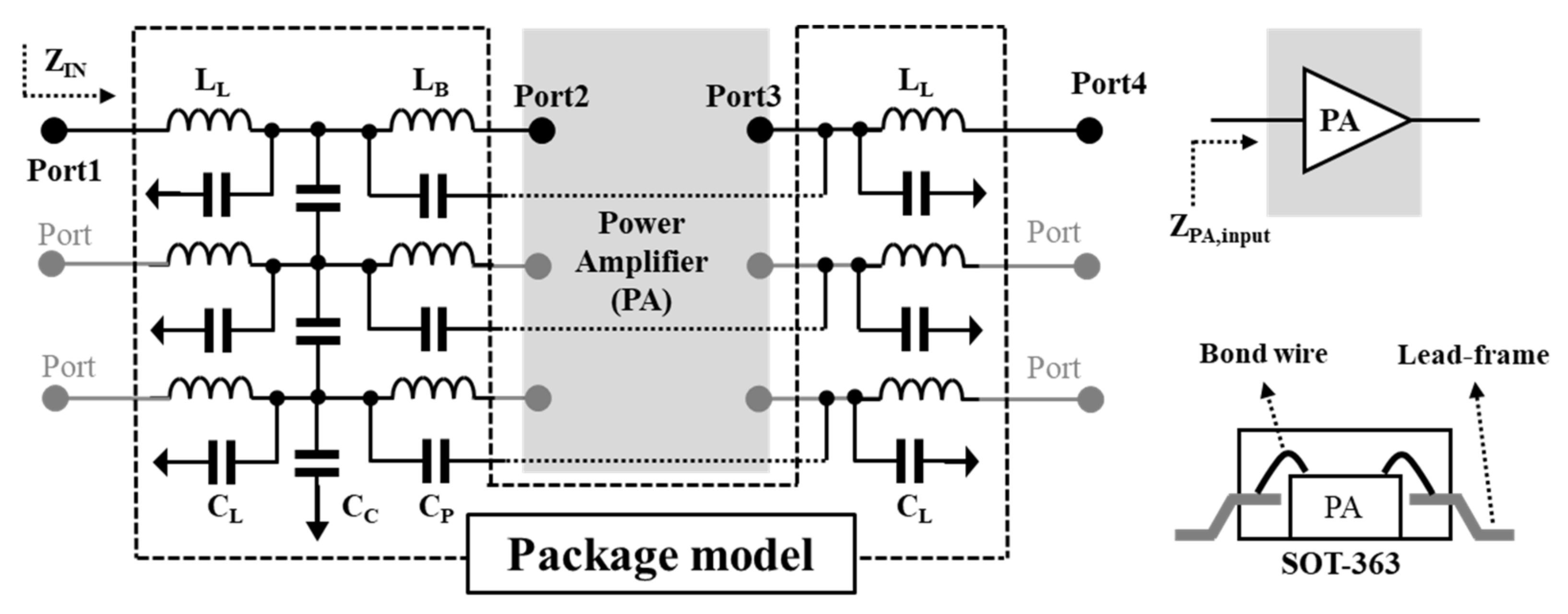
2.1. Package Model for SOT-363
Figure 1 shows the equivalent linear model for a small outline transistor (SOT) package, which is widely used for low-cost general-purpose amplifiers. In general, the package model using the lead-frame has equivalent to lead-frame inductance (L
L) and capacitance (C
L), bond wire inductance (L
B), package capacitance (Cp), and coupling capacitance (Cc).
Table 1 presents the element values for the package model up to 6 GHz. It is shown that the inductances modeled by L
L and L
B have a larger element value than other equivalent elements [
14].
These inductances can change the impedance at high frequencies, which can degrade the high-frequency corner performance of a broadband amplifier. If the input impedance of the amplifier is
ZPA,input, it is expressed as follows:
Here,
Rinput_opt and
Xinput_opt are assumed to be the optimal real and imaginary impedance for the amplifier, respectively. As shown in Equation (1), if the input impedance of the amplifier includes the equivalent circuit model from the package, it can be expressed as follows (2):
Here, C
L, C
P, and C
C can be neglected because they have an insignificant effect on the impedance variation in the desired frequency band. As such, the package model changes the imaginary part of the amplifier’s input impedance, which will degrade the performance as the frequency increases.
Figure 2 shows the S-parameter results of the package model according to frequency using the ports in
Figure 1. As shown in the results, the model of the package is simulated with impedance varying up to high frequency, which can change the high-frequency response characteristics of the amplifier.
If the amplifier does not use an external matching network and has an integrated matching network, the amplifier has an insertion loss (S
21) of up to 0.6 dB at 5 GHz. Conversely, in the case of an amplifier using an external matching network, the equivalent circuit model of the package can affect the impedance matching condition for the optimal impedance of the amplifier. Furthermore, the port isolations of S
31 and S
41 from DC to 5 GHz have below −30 dB in
Figure 2a. However, in the case of 5 GHz or higher, the port isolation is lowered to more than –30 dB due to package effect. Therefore, the equivalent model for the package should be sufficiently considered for the broadband characteristics.
2.2. Diode Model for ESD Portection
For mass-produced products, general electronic components have standards for ESD protection level, and amplifier components must satisfy a Class-1C standard of 2000 V based on HBM (human body model) standards [
3,
4,
5].
For ESD protection circuits, the stacked diode is widely used for amplifier IC. For the HBM simulation in
Figure 3, the test-bench consists of a 1.5 kΩ resistor (R
2), a 100-pF capacitor, and an 8 μH series inductor [
15]. The current peak is typically 1.2–1.48 A for 2000 V HBM ESD stress. Here, the stacked diode protects the internal circuit by forming an instantaneous current path above the voltage of V
th × n (n is the number of the stacked diode). However, the diode model supported by the manufacturer does not include parameters for a large signal, which can cause DC convergence error in simulation, thereby lowering the accuracy of the simulation result. Therefore, in the simulation of the amplifier, it is necessary to apply the equivalent circuit model to predict the impedance variation. Here, a simple model for the stacked diode can consist of capacitance (C
Diode) and resistance (R
Diode).
Table 2 shows the input and output stacked diode sizes and equivalent element values used in the design, and stacked diodes are paralleled forward and reverse to protect the internal IC circuitry from high voltages in ESD events. As shown in
Table 2, the ESD protection diode sizes for a 2000 V HBM at the input and output requires 4-stacked diodes of 150 μm size and 16-stacked diodes of 200 μm size, which are equivalent to 0.502 pF and 1.65 Ω and 0.46 pF and 2.35 Ω, respectively.
As shown in
Figure 4, the model of the ESD-protected diode can be equivalent to the series connection model of
RDIODE,S and
CDIODE,S. Here, if the impedance of the series equivalent model is converted to a parallel equivalent circuit,
CDIODE,S and
RDIODE,S can be expressed as
CDIODE,P and
RDIODE,P. Of course, the impedance transformation cannot remain the same at all frequencies. However, it is possible to model the effect of the package and the stacked diode in the narrowband frequency range of the desired edge frequency. For impedance transformation, it is briefly expressed as follows.
If the series section is converted into a parallel section, as in Equations (3) and (4), the Q is 32 at 6 GHz and the RDIODE,P is ignored because the resistance value is large. Additionally, because CDIODE,P has the same value as CDIODE,S, it can be an equivalent circuit to LPACKAGE and CDIODE,P, which has the response characteristic of a low-pass filter. This can limit the bandwidth of the amplifier at the edge-frequency.
Figure 5 shows the results with and without the equivalent circuit for ESD in the package model. As such, the equivalent circuit model of the ESD-protected stacked diodes changes the impedance over high frequencies. Therefore, it must be considered when designing a broadband amplifier.
2.3. Cascode Gain Amplifier with the Feedback Resistor
In general, the common-source (CS) amplifier, which is commonly used for transconductance amplifiers, uses one transistor and has a simple structure. However, it has a limited bandwidth due to the Miller effect at high frequency. On the other hand, the cascade amplifier is a two-stage amplifier consisting of a common-source (CS) and a common-gate (CG). This is the advantage of minimizing the Miller effect caused by the CS amplifier with the Cgs of the CG amplifier, which is widely applied in high-frequency applications.
Figure 6 shows the maximum available gain (MAG) according to a single common-source and cascode structure. Here, the transistor was used using 0.5 μm GaAs E-pHEMT. The feedback method has been widely applied to broadband amplifiers because it can have flat gain and high linearity. However, the bandwidth is determined by the gain response characteristic of the amplifier itself. Therefore, the structure of the amplifier having a high gain response for broadband bandwidth is advantageous. As shown in
Figure 6, for a broadband amplifier with a gain of 20 dB or more, a single common source structure cannot satisfy the performance above 3 GHz. However, the cascode structure exhibits a high gain of about 30 dB up to 6 GHz or higher, so it is suitable as a structure for feedback.
Figure 7 shows the MAG and input impedance variation according to the feedback resistance. As shown in
Figure 7a, the gain of the cascode amplifier using a 500 Ω feedback resistor was more than 20 dB up to 5 GHz. Additionally, as shown in
Figure 7b, the S
11 of the cascode amplifier without feedback has a large impedance varying range in the desired frequency range, making it difficult to match the optimal impedance using the general narrowband matching network. However, when the feedback method is used, the impedance varying range change is relatively small, so impedance matching is possible with a general matching network.
3. Design and Simulation Results
Figure 8 shows the evaluation board of the proposed broadband gain block amplifier with a feedback resistor and the proposed amplifier design applied to the equivalent circuit model of the package and ESD-protected stacked diode for robustness. It has a cascode structure with gate length of M
1 and M
2 transistor cells of 12 × 75 μm and 10 × 75 μm, respectively. A simple matching network of inductance and capacitance is constructed for impedance matching in addition to the feedback resistor and bias circuit. For the simulation, a 0.5 μm GaAs E-mode pHEMT PDK (Process design kit) of Win-semiconductor was used in the ADS (Advanced Design System of Keysight technologies) simulator, and all the devices used in the circuit were applied by replacing them with the s-parameter model using the ADS momentum simulator. In particular, the external matching inductance of the evaluation board uses a value fixed of 100 nH in the desired frequency band.
The layout in
Figure 9 includes input and degeneration inductances for input impedance matching and an inductance for output matching. It also includes a stacked diode on the input and output pad for ESD protection. In the layout, inductance is a necessary component for impedance matching. However, the capacitance coupling between them can make a difference between the simulation result and the actual measurement result, which can degrade the performance of the amplifier. To minimize the effect of coupling between inductances, it was optimized using the ADS momentum simulator.
Table 3 shows the coupling ratio between inductances using the ADS EM simulator, where the distance between the inductors is indicated as D
1, D
2, and D
3, and their capacitive coupling effect is also described. In the case of the initial layout, the distance between the output inductance and degeneration inductance was 33.5 μm, which had a coupling ratio of about 27.8 dB. However, the coupling path between the amplifier output and the degenerate inductance can lead to gain degradation by forming an undesirable feedback path. Therefore, the distance between inductances was increased for a coupling ratio of –32.3 dB, which is improved by 4.5 dB.
Figure 10 shows the simulation results of the designed broadband gain amplifier. The gain flatness in
Figure 10a was 1.92 dB up to the 5 GHz frequency band, and S
11 and S
22 were matched below −9.2 dB. For the matching network, a low-pass network and a feedback technique were applied.
Figure 10b shows the matching condition of input and output. Except for the low frequency of 50 MHz, the designed broadband amplifier at the desired frequency band was matched under good matching conditions near a voltage standing wave ratio (VSWR) of 2.
Additionally, the P
1dB and OIP
3 exhibited 15.3 to 16.9 dBm and 26.5 to 31 dBm in
Figure 10c, respectively.
The performances are summarized and compared to existing products and papers in
Table 4. The designed amplifier showed excellent results, with low power consumption, high gain, and flat gain characteristics. The designed broadband amplifier exhibited a gain of 18.7 dB ± 1.92 dB with a small flatness and a low dc power consumption of 156 mW. It also achieved a 1dB compression point and a OIP
3 of 15.7 dBm and 27.5 dBm, respectively. The noise figure was 1.61 dB at 2650 MHz frequency.
4. Conclusions
In this paper, a broadband gain amplifier was designed with the equivalent circuit models of the package and stacked diode. It had a cascode structure with a feedback technique for high gain and broadband characteristics. The applied cascode structure had the advantage of being able to use a high gain in a wide band range compared to the commonly used common source structure. In addition, the design considering the impedance change is shown by applying the equivalent circuit of the package and ESD diode that limits the bandwidth of the broadband amplifier. The proposed broadband gain amplifier was designed using a 0.5 μm GaAs E-pHEMT process, and a gain of 18.7 dB to 20.6 dB, a P1dB of 15.3 to 16.9 dBm, and an OIP3 of 26.5 to 31 dBm were simulated. Additionally, it achieved gain flatness within 1.92dB.


