Abstract
Improving semiconductor equipment and components is an important goal of semiconductor manufacture. Especially during the deposition process, the temperature of the wafer must be precisely controlled to form a uniform thin film. In the conventional plasma-enhanced chemical vapor deposition (PECVD) chuck, heating rate, and temperature uniformity are limited by the spiral pattern and volume of the heating element. To overcome the structural limitation of the heating element of conventional chuck, we tried to develop the planar heating chuck (PHC), a 6-inch PECVD chuck with a planar heating element based on NiCr thin film that would be a good candidate for rapidly and uniformly heating. The time for the temperature elevation from room temperature to 330 °C was 398 s. In a performance evaluation, the fabricated PHC successfully completed a SiO2 PECVD process.
1. Introduction
Plasma-enhanced chemical vapor deposition (PECVD) is one of the major deposition processes for fabricating various thin films such as oxide–nitride–oxide–nitride films, amorphous carbon layers, and antireflective coatings used in three-dimensional vertical NAND flash memory and other semiconductor devices [1,2,3]. The increasing demand for memory devices with expanded storage capacity [4] has driven the need for highly stacked uniform thin films [5], which require the precise control of the temperature of wafers during the PECVD process. Because temperature uniformity and the ramping-up/-down rata of the PECVD equipment critically determine yield and fabrication throughput [6,7,8,9,10,11], they are the main evaluation criteria of the capability of PECVD equipment and wafer chucks (or heaters).
The wafer temperature in the PECVD chamber is usually controlled by a chuck that directly supports the wafer. Typical PECVD chucks contain a resistance heating element constructed from a metal wire or metal thin film shaped into a spiral coil. However, as these types of chucks are structurally constrained, they degrade the temperature uniformity at high temperatures and heating rates. With the recent demand for high-performance heaters with good temperature uniformity and rapid heating rates during the deposition process, these issues have become problematic. The poor temperature uniformity problem has been overcome using the multi-zone method, which divides the zones of the heater and differently heats them by area [12].
Our PECVD R&D tool for dielectric deposition processing has a 6-inch wafer capacity and the heating element consists of a spiral coil; we had suffered from the temperature uniformity over the 6-inch wafer as well as prolonged heating time for the deposition process. In many cases of academic research, wafer uniformity is a secondary priority of concern because a small-sized coupon is preferable for material characterization and device fabrication. However, whole wafer processing is necessary for the consideration of equipment performance enhancement and semiconductor manufacturing aspect.
To overcome the thermal disadvantages of the conventional PECVD chuck, we applied a planar heating element to the chuck, which we called the planar heating chuck (PHC) and which is composed of conductive materials formed into thin films. These planar structures are advantageous in terms of rapid heating rate and uniform heating of the wafers. Nichrome (NiCr) thin film is an excellent candidate for the heating element owing to its high corrosion resistance, oxidation resistance, and low-temperature coefficient of resistance [13]. Moreover, NiCr thin film can be applied in various shape and form to improve temperature uniformity and can be rapidly heated at rates exceeding 50 °C/s based on a technical report High-End Technology Co., Ltd. that provided deposition technology of NiCr thin film in this study.
In this study, we fabricated and evaluated a 6-inch PECVD PHC with a NiCr thin film as the heating element and doughnut-shaped electrodes for rapid and uniform heating to 300 °C. In the feasibility test and performance evaluations of the PHC, the temperature distribution, heating rate, and silicon oxide deposition were evaluated after mounting PHC on the PECVD equipment, which is a capacitively coupled plasma system, as shown Figure 1. In our previous study, we designed a PHC with doughnut-shaped electrodes and a disk-shaped planar heating element, as shown in Figure 2 [14]. The previously designed resistance of the NiCr thin film was checked in a heat treatment test of the film. Based on our previous simulation study and the measured resistance change, we verified the performance of our fabricated PHC.
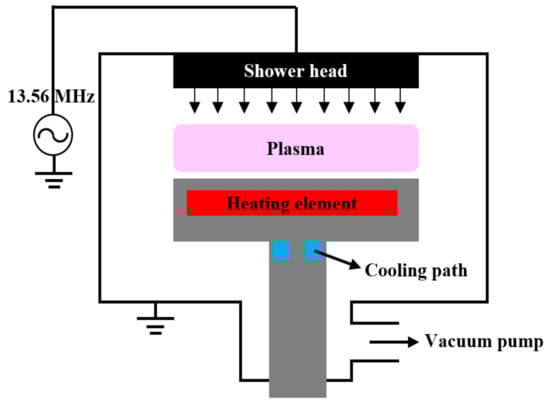
Figure 1.
Schematic of the PECVD equipment.
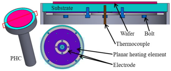
Figure 2.
PHC structures designed in our previous study [14]. ©2020 The Japan Society of Applied Physics.
2. PHC Fabrication
The PHC structure and power were designed based on the pre-simulation results. Similarly, the electrical interface of the bottom side of the PHC was fabricated in the same form as the existing chuck mounting our PECVD equipment to carry out PECVD test of the PHC. Before fabricating PHC, resistance change depending on the heat treatment condition was analyzed to use a nichrome thin film as the planar heating element. Figure 3 shows the process flow for PHC fabrication.
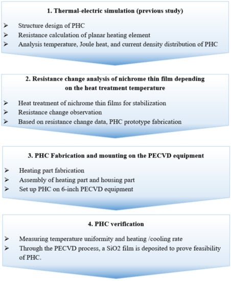
Figure 3.
Process flow for PHC fabrication.
2.1. Heating Element
The NiCr thin film as a heating element was formed using the sputtering deposition method on the bottom side of the aluminum nitride PHC substrate. The deposition thickness was a few hundred nanometers. In a heater that precisely regulates temperature, we must control the resistance of the heating element. However, the resistance of the NiCr thin film is sensitive to the following heat treatment conditions: temperature, time, and atmosphere of the treatment. In fact, the resistance (or resistivity) of films with thicknesses of several hundred nanometers can be changed by other factors, such as oxidation and crystal structure change [15,16]. To control the resistance, the deposited thin film should be treated at a temperature higher than the operating temperature of the PHC [13,17,18]. We thus measured the sheet resistance dependence of the NiCr thin film under different heat treatment conditions.
The heat treatment conditions are shown in Table 1. We prepared 20 mm × 20 mm diced specimens from a 6-inch silicon oxide wafer sputter-deposited with the thickness of 50 nm of NiCr thin film. The NiCr was deposited using a customized sputtering system. To observe the changes in the sheet resistance over a wide range of heat treatment temperatures, we divided the heat treatment temperature into 200 °C intervals. During the heat treatment, the oxidation of the NiCr thin film was minimized by nitrogen purging. To reduce the time and cost of the process, we used a silicon oxide wafer for the substrate of heat treatment test instead of the aluminum nitride substrate of PHC. The surface oxidation of the nickel and chrome undesirably increases the resistance of the NiCr thin film by reducing the thickness of the conductive layer and by reducing the number of nickel and chrome atoms, which participate in electric conduction [19]. Heat treatment was performed in a tube, and the sheet resistance was measured by a four-point probe. For the thermal treatment of the NiCr thin film, the specimens were positioned in the furnace tube, as shown in Figure 4.

Table 1.
Heat treatment test conditions.
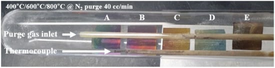
Figure 4.
Placement of specimens in the furnace tube. Specimen positions in the tube furnace are indicated by (A–E). (E) is placed near the cap, and (A) is inside.
Figure 5 shows the measured changes in the NiCr sheet resistance. The specimens heat-treated at the same temperature showed different sheet resistances, probably because they were heated to different temperatures in the tube furnace with poor temperature uniformity. The specimens at position A, located near the innermost part of the tube, were heat-treated to a higher temperature than those placed at position E near the cap (Figure 4). As shown in Figure 5, the sheet resistances of the specimens heat-treated at 800 °C were high and widely variable. It was assumed that the parts of the NiCr thin film were severely oxidized at 800 °C despite N2 purging. Consequently, the NiCr thin film was unsuitable as a heating element at temperatures around 800 °C. After heat treatment at 600 °C, the sheet resistances were reduced from those of the as-deposited specimens. This result was assumed to be the dominant recrystallization of the NiCr thin film (which reduced the resistance) over oxidation (which raised the resistance). During heat treatment, N2 purging minimizes the oxidation. The same trend was observed at positions D and E at 800 °C (Figure 5), which actually have been heat-treated to below 800 °C. The resistance of the NiCr thin film certainly decreased until around 600 °C.
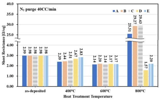
Figure 5.
Resistance variation of NiCr thin films after different heat treatment temperatures.
2.2. Electrode
Among various candidate materials, silver paste is suitable for the PHC electrode material, because it has high-temperature oxidation resistance and good conductivity at high temperatures and is easily formed into the desired shape [20,21,22,23]. Considering the heat treatment temperature of the planar heating element, we selected silver paste sintered at 550 °C as the electrode material, which has been commercially proven by outsourcing. Accordingly, the heating part of the PHC prototype, comprising the aluminum nitride substrate, planar heating element, and electrodes, was heat-treated at 550 °C (see Figure 6 for the finished product). After the heat treatment, the resistance between the electrodes was measured to be 0.46 ohms.
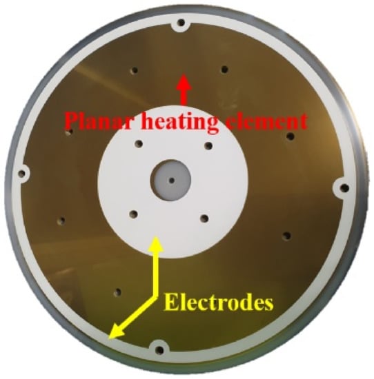
Figure 6.
Heating part of the PHC prototype heat-treated at 550 °C.
2.3. Housing Assembly
Figure 7 shows the parts and assembled form of the PHC. Figure 7a shows the electrical connection of the planar heating element, electrodes, and wires. A silver paste was printed on the surface of the planar heating element and then fired to form electrodes. Taps were placed on the substrate to couple the O-ring type terminal (connected with wire) to the electrodes with ceramic bolts. The housing part consists of a metal body containing shafts, a cooling path, heater connector, and a thermocouple, as shown in Figure 7b. The substrate and housing of the PHC were fixed with a stainless steel band during the performance test due to a design error. The PHC substrate was aluminum nitride, which has various advantages as a substrate material [24], including high thermal conductivity, which improves the temperature uniformity, as shown in Figure 7c. To carry out PECVD process test of PHC, PHC was fabricated in the same shape as the existing heater of our PECVD equipment, as shown in Figure 7d. The thermocouple connected to a power supply was contacted with the center of the PHC substrate, as shown in Figure 2. The power supply controls the temperature using the proportional integral derivative (PID) method.
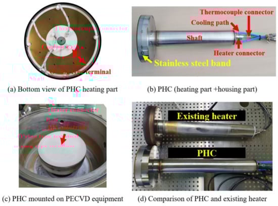
Figure 7.
PHC assembly and mounting form.
3. PHC Performance Verification
The temperature distribution was measured at 17 points on the wafer surface with a contact thermometer (TES-1300, TES Electrical Electronic Corp., Taipei, Taiwan), and the results are displayed in Figure 8. The temperature of wafers on the PHC was measured by opening the chamber 5 min after the temperature of PHC reached to 300 °C. The average and standard deviation of the wafer temperatures were 304.1 °C and 3.1 °C, respectively. Figure 9 compares the results of a prior simulation study and the temperature measurements on the PHC wafer. As the measured average temperature was 304.1 °C, we raised the temperature in the simulation (originally set at 300 °C) by 4.1 °C for a proper comparison. Figure 8 and Figure 9 show the temperature distribution results of a higher difference than the simulation. This seems to increase the error when measuring the temperature due to non-uniform thermal contact resistance by the pasting condition. Because the employed PHC is a prototype, the wafer cannot be clamped like an electrostatic chuck. This causes different thermal resistance between the PHC and wafer depending on the pressure of each measurement point. The thickness uniformity of NiCr thin film by sputtering deposition also determines the temperature uniformity of the PHC. As a result, large temperature measurements error may occur. These issues need to be solved in further studies.
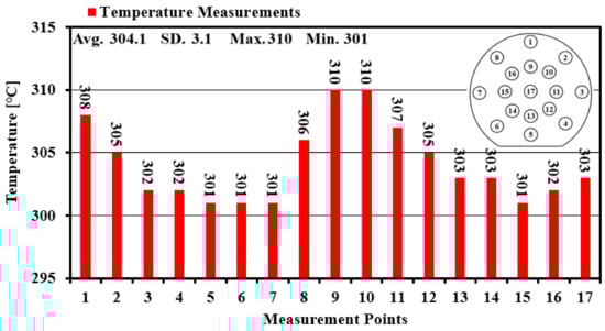
Figure 8.
Measured temperature distribution across the wafer.
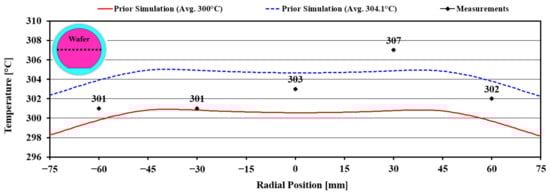
Figure 9.
Comparison of horizontal temperature variation between a previous simulation study in solid lines and the present measurements in dotted points.
As our PECVD equipment was under PID control, only the PHC heating parts (excluding the housing part) were tested using a power supply and transformer. The results of the heating rate test are shown in Table 2. At 80% of the maximum power (approximately 1250 W), the PHC heating part was heated from 25 °C to 330 °C in 6 min and 38 s (a heating rate of approximately 45.9 °C/min). The cooling rate was measured using the PECVD equipment. The designed cooling path of the PHC (see Figure 1) was the same as the original equipment manufactured heater. The cooling capacity of the chiller was 1.46 kW, and the setting temperature of the coolant was 19.8 °C. The cooling rate of the PHC, measured in a 40 mTorr vacuum chamber, while the PECVD equipment monitor of the heater fell from 300 °C to 100 °C, was 4.1 °C/min. Actually, the heating/cooling rate of a heater is influenced by various factors such as allowable power, heating/cooling system, heater structure, heating element materials, and parts material like the substrate. In this study, since PHC was designed for the main purpose of the feasibility test during PECVD process, the heating rate of the PHC was insufficient compared to the heating rate of the nichrome thin film. There are various ways to improve the heating rate to heating rate of nichrome thin film by changing PHC structure, substrate dimension, heating parts structure. In future studies, the goal is to improve the heating rate of PHC to about the heating rate of the nichrome thin film.
Table 2.
Heating rate test of the PHC heating part.
The feasibility of the PHC was measured in a SiO2 process with the PECVD equipment. The deposition thickness of the SiO2 film was measured using a reflectometer (ST2000-DLX, KMAC Co., Ltd., Daejeon, Korea) after the PECVD process. Figure 10 presents the thickness changes of SiO2 over position and time. We indirectly checked the functional operation and uniform heating of PHCs with different deposition thicknesses (varied by changing the processing time). Any problems related to the structure and material of the PHC can change the temperature uniformity, manifesting as significantly increased deviations in the deposition thickness. The average deposition thickness obviously increased with processing time, and the average thickness differences were similar to those of a regular chuck during operation (data not shown). The standard deviation of the thickness was greater at 180 s than at 60 s, possibly because of the partial defects in the PHC. Such deviations can also be caused by factors such as the condition of the showerhead and equipment and the function of the chuck. Additional experiments are needed for accurate evaluation.
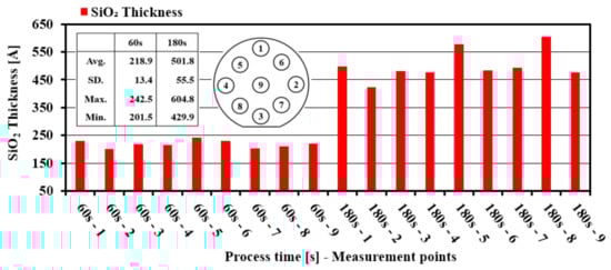
Figure 10.
Deposition thickness changes in SiO2 at different process times.
4. Conclusions
This study investigated our PHC with a planar heating element, which can heat a wafer to a uniform temperature at a rapid heating rate. The PHC successfully completed a PECVD process with a heating rate of 45.9 °C/min. The temperature of the heated wafer deviated between 301 °C and 310 °C, averaging 304.1 °C. To test the NiCr thin film as the planar heating element of the PHC, we measured the NiCr resistance response to different heat treatment conditions. The sheet resistance tended to decrease until the temperature reached 600 °C and then rapidly increased. This change was attributed to various causes, such as recrystallization, oxidation, and the formation of an oxide layer on the surface. To accurately control of resistance of the nichrome thin film (used as the planar heating element of PHC), mechanism analysis on the resistance change depending on the heat treatment condition is the topic of ongoing research. In this study, we focused on confirming the possibility of PHC in operation. Thus, further studies are planned to prove essential factors to use PHC as commercial PECVD heaters.
Author Contributions
Conceptualization, principal investigation, and supervision, funding acquisition, writing—review and editing, S.-J.H.; methodology, visualization, data curation, writing—original draft preparation, D.-H.I., T.-W.Y. and W.-S.M. All authors have read and agreed to the published version of the manuscript.
Funding
This work was supported by the grant funded by Gyeonggido R&D grant (G14AICT06T10001).
Acknowledgments
This work was supported by the Korean Ministry of Trade, Industry and Energy (MOTIE) via Advanced Institute of Convergence Technology (GID: AICT 006-T1), and the authors are grateful to High-end Technology, Korea, for numerous technical discussions on the fabrication.
Conflicts of Interest
The authors declare no conflict of interest.
References
- Kaloyeros, A.E.; Jové, F.A.; Goff, J.; Arkles, B. Review—silicon nitride and silicon nitride-rich thin film technologies: Trends in deposition techniques and related applications. ECS J. Solid State Sci. Technol. 2017, 6, P691–P714. [Google Scholar] [CrossRef]
- Li, H.; Higuchi, H.; Kawaguchi, S.; Satoh, K.; Denpoh, K. Computational study on silicon oxide plasma enhanced chemical vapor deposition (PECVD) process using tetraethoxysilane/oxygen/argon/ helium. Jpn. J. Appl. Phys. 2019, 58, SEED06. [Google Scholar] [CrossRef]
- Kwon, S.; Park, Y.; Ban, W.; Youn, C.; Lee, S.; Yang, J.; Jung, D.; Choi, T. Effect of plasma power on properties of hydrogenated amorphous silicon carbide hardmask films deposited by PECVD. Vacuum 2020, 174, 109187. [Google Scholar] [CrossRef]
- Moore, M. International Roadmap for Devices and Systems 2018, 2018. Roadmap Report. Available online: https://irds.ieee.org/editions/2018 (accessed on 25 January 2021).
- Jang, D.B.; Hong, S.J. In-Situ monitoring of multiple oxide/nitride dielectric stack pecvd deposition process. Trans. Electr. Electron. Mater. 2018, 19, 21–26. [Google Scholar] [CrossRef]
- Olson, K.A.; Kotecki, D.E.; Ricci, A.J.; Lassig, S.E.; Husain, A. Characterization, modeling, and design of an electrostatic chuck with improved wafer temperature uniformity. Rev. Sci. Instrum. 1995, 66, 1108–1114. [Google Scholar] [CrossRef]
- Engelmann, J.; Chu, D.; Dupraz, T.; Haupt, R.; Hennesthal, C.; Pflug, H.; Jaschke, V.; Stadel, M. Measuring the wafer temperature in CVD tools using the wireless SensArray HighTemp-400 wafer. In Proceedings of the IEEE 2017 28th Annual SEMI Advanced Semiconductor Manufacturing Conference, New York, NY, USA, 15–18 May 2017; pp. 161–164. [Google Scholar]
- Zhiming, L.; Hailing, L.; Xiaobing, G.; Haiying, J.; Jinping, L.; Xiaoqian, F.; Yanbin, H.; Yingjie, X.; Jianqin, Y.; Yimei, H.; et al. A susceptor with a Λ-shaped slot in a vertical MOCVD reactor by induction heating. J. Semicond. 2014, 35, 092003. [Google Scholar]
- Shan, H.; Pu, B.Y.; Gao, H.; Ke, K.H.; Lewis, J.; Welch, M.; Deshpandey, C. Process kit and wafer temperature effects on dielectric etch rate and uniformity of electrostatic chuck. J. Vac. Sci. Technol. B 1996, 14, 521–526. [Google Scholar] [CrossRef]
- Hsu, K.-C.; Yang, J.-Y.; Chen, J.-Z.; Yu, Y.-H.; Chen, Y.-J. Modeling and simulation of heat transfer characteristics of 12-inch wafer on electrostatic chuck. In Proceedings of the 2015 10th International Microsystems, Packaging, Assembly and Circuits Technology Conference (IMPACT), Taipei, Taiwan, 21–23 October 2015; pp. 304–307. [Google Scholar]
- Kanno, S.; Edamura, M.; Yoshioka, K.; Nishio, R.; Kanai, S.; Kihara, H.; Shimada, T. High-temperature electrostatic chuck for nonvolatile materials dry etch. J. Vac. Sci. Technol. B Microelectron. Nanometer Struct. 2005, 23, 113. [Google Scholar] [CrossRef]
- Woo, D.S.; Han, C.; Youn, B.D.; Kim, K.J. Thermal modelling and design of dynamically-controlled heater plates for high temperature processing of 300 mm wafers. J. Mech. Sci. Technol. 2019, 33, 5009–5016. [Google Scholar] [CrossRef]
- Das, S.; Akhtar, J. Comparative study on temperature coefficient of resistance(TCR) of the E-beam and sputter deposited nichrome thin film for precise temperature control of microheater for MEMS gas sensor. In Physics of Semiconductor Devices. Environmental Science and Engineering; Jain, V., Verma, A., Eds.; Springer: Berlin/Heidelberg, Germany, 2014; pp. 495–497. ISBN 978-3-319-03002-9. [Google Scholar]
- Im, D.-H.; Min, W.-S.; Hong, S.-J. Planar heating chuck to improve temperature uniformity of plasma processing equipment. Jpn. J. Appl. Phys. 2020, 59, SJJD01. [Google Scholar] [CrossRef]
- Lane, C.H. Nichrome Resistor Properties and Reliability; Technical Report; AD076553; Rome Air Development Center, Air Force Systems Command, Griffiss Air Force Base: New York, NY, USA, 1973; Available online: https://apps.dtic.mil/sti/citations/AD0765534 (accessed on 25 January 2021).
- Phuong, N.; Lee, W.; Yoon, S. Thickness dependence of the electrical properties in NiCr thin film resistors annealed in a vacuum ambient for π—type attenuator applications. J. Korean Inst. Electr. Electron. Mater. Eng. 2006, 19, 712–716. [Google Scholar] [CrossRef][Green Version]
- Yan, J.; Zhou, J. Strain sensitivity and temperature influence of nichrome(80/20 wt.%) thin film fabricated by magnetron sputtering. Int. J. Mod. Phys. B 2007, 21, 3719–3731. [Google Scholar] [CrossRef]
- Feil, M.; Mader, W. Investigation of the adhesion mechanism of NiCr layers on Al2O3 and AlN substrates. In Proceedings of the IEEE 1991 41st Electronic Components and Technology Conference, Atlanta, GA, USA, 11–16 May 1991; pp. 134–140. [Google Scholar]
- Kwon, Y.; Kim, N.-H.; Choi, G.-P.; Lee, W.-S.; Seo, Y.-J.; Park, J. Structural and surface properties of NiCr thin films prepared by DC magnetron sputtering under variation of annealing conditions. Microelectron. Eng. 2005, 82, 314–320. [Google Scholar] [CrossRef]
- Bai, J.G.; Zhang, Z.Z.; Calata, J.N.; Lu, G.-Q. Low-temperature sintered nanoscale silver as a novel semiconductor device-metallized substrate interconnect material. IEEE Trans. Compon. Packag. Technol. 2006, 29, 589–593. [Google Scholar] [CrossRef]
- Ordonez-Miranda, J.; Hermens, M.; Nikitin, I.; Kouznetsova, V.G.; van der Sluis, O.; Ras, M.A.; Reparaz, J.; Wagner, M.; Sledzinska, M.; Gomis-Bresco, J.; et al. Measurement and modeling of the effective thermal conductivity of sintered silver pastes. Int. J. Therm. Sci. 2016, 108, 185–194. [Google Scholar] [CrossRef]
- Rane, S.; Puri, V.; Amalnerkar, D. A study on sintering and microstructure development of fritless silver thick film conductors. J. Mater. Sci. Mater. Electron. 2000, 11, 667–674. [Google Scholar] [CrossRef]
- Chang, C.-R.; Jean, J.-H. Effects of silver-paste formulation on camber development during the cofiring of a silver-based, low-temperature-cofired ceramic package. J. Am. Ceram. Soc. 2005, 81, 2805–2814. [Google Scholar] [CrossRef]
- Kurokawa, Y.; Utsumi, K.; Takamizawa, H. Development and microstructural characterization of high-thermal-conductivity aluminum nitride ceramics. J. Am. Ceram. Soc. 1988, 71, 588–594. [Google Scholar] [CrossRef]
Publisher’s Note: MDPI stays neutral with regard to jurisdictional claims in published maps and institutional affiliations. |
© 2021 by the authors. Licensee MDPI, Basel, Switzerland. This article is an open access article distributed under the terms and conditions of the Creative Commons Attribution (CC BY) license (https://creativecommons.org/licenses/by/4.0/).