
The Fourth-Order Single-Switch Improved Super-Boost Converter with Reduced Input Current Ripple


 ,
,  ,
,  and
and
Abstract
:1. Introduction
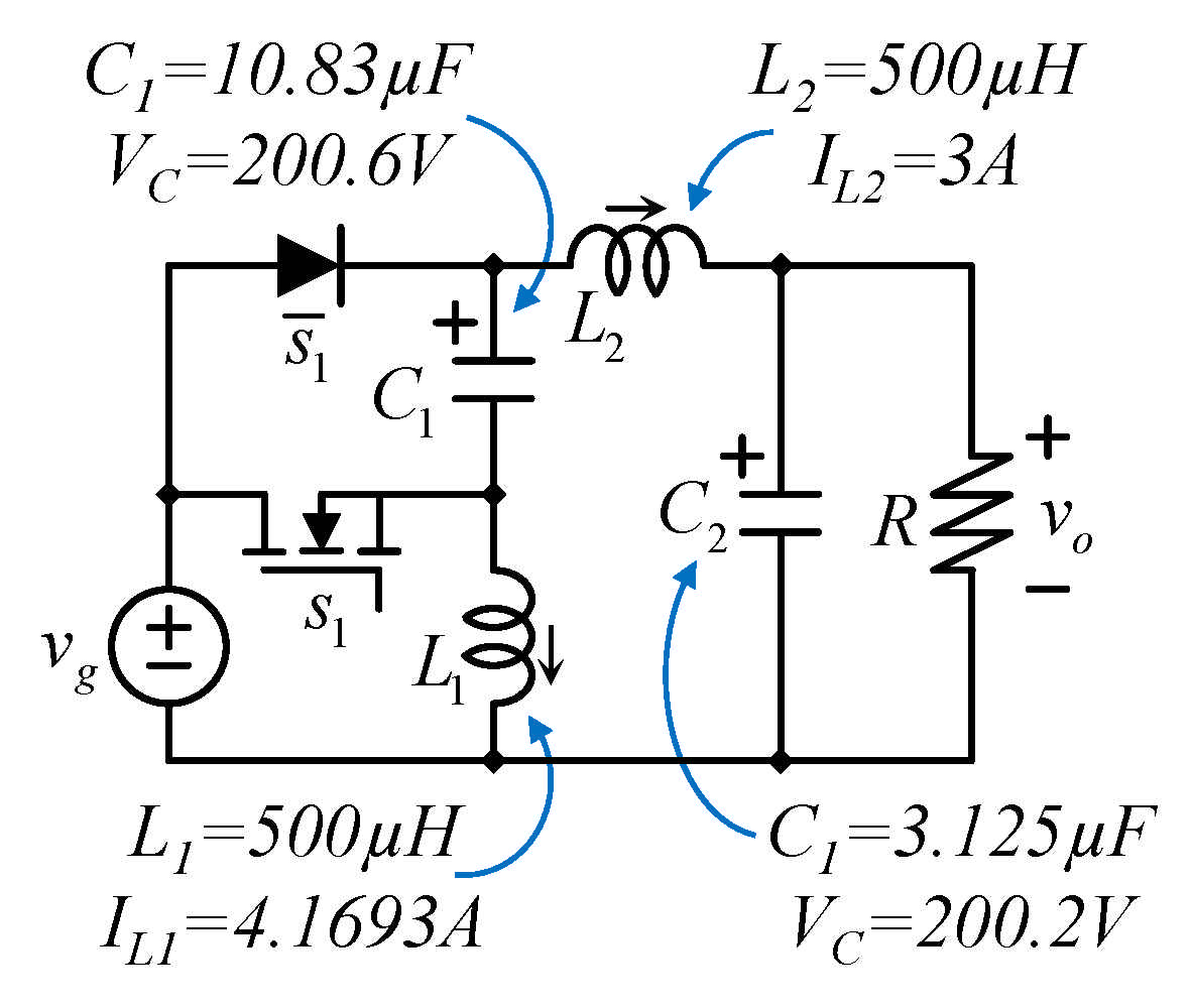
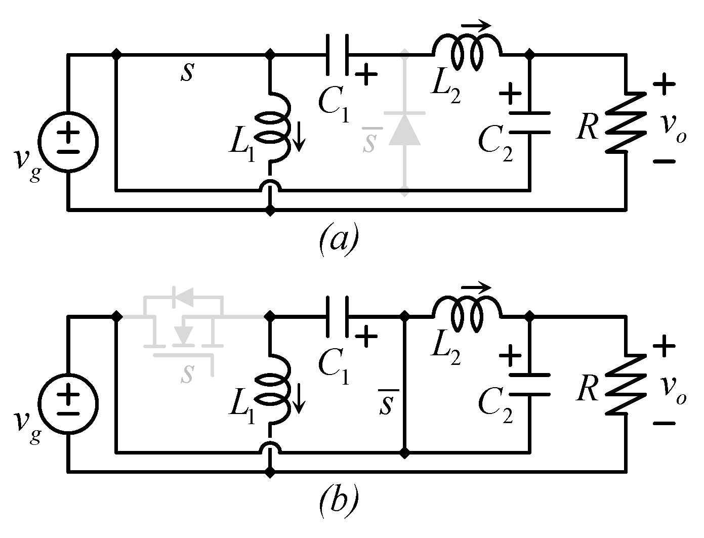
2. The Super-Boost Converter
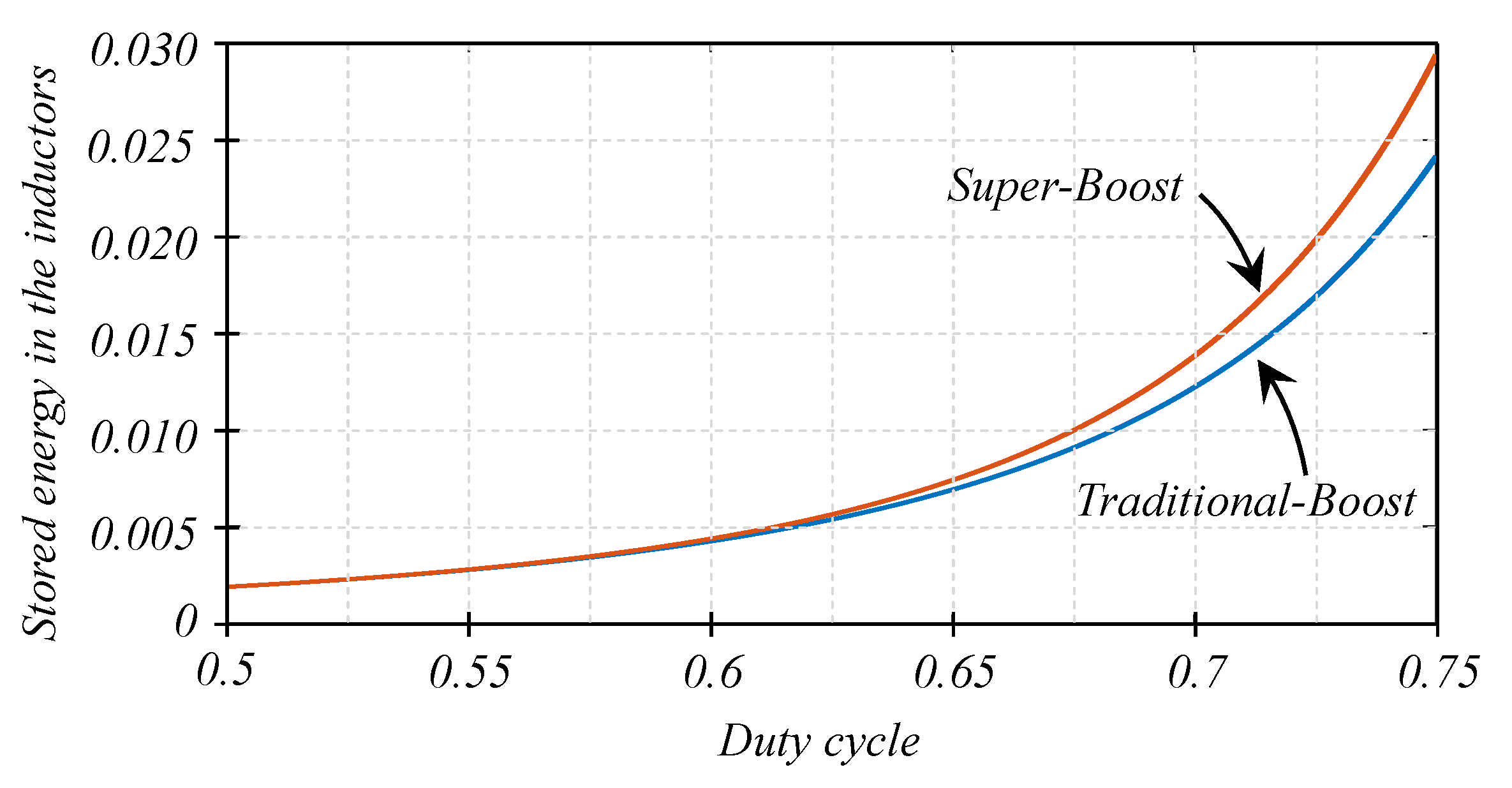
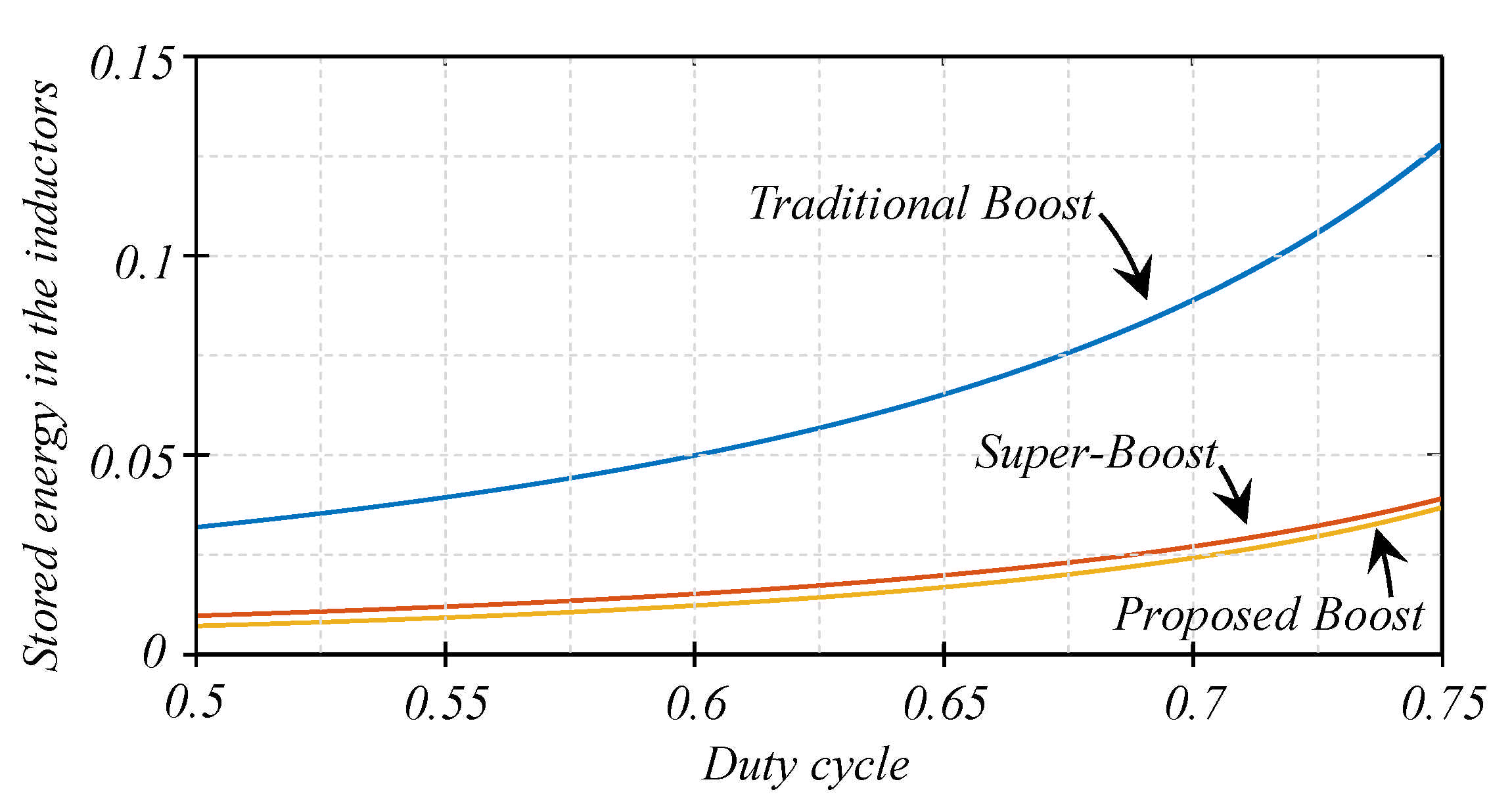
2.1. Stored Energy in Inductors
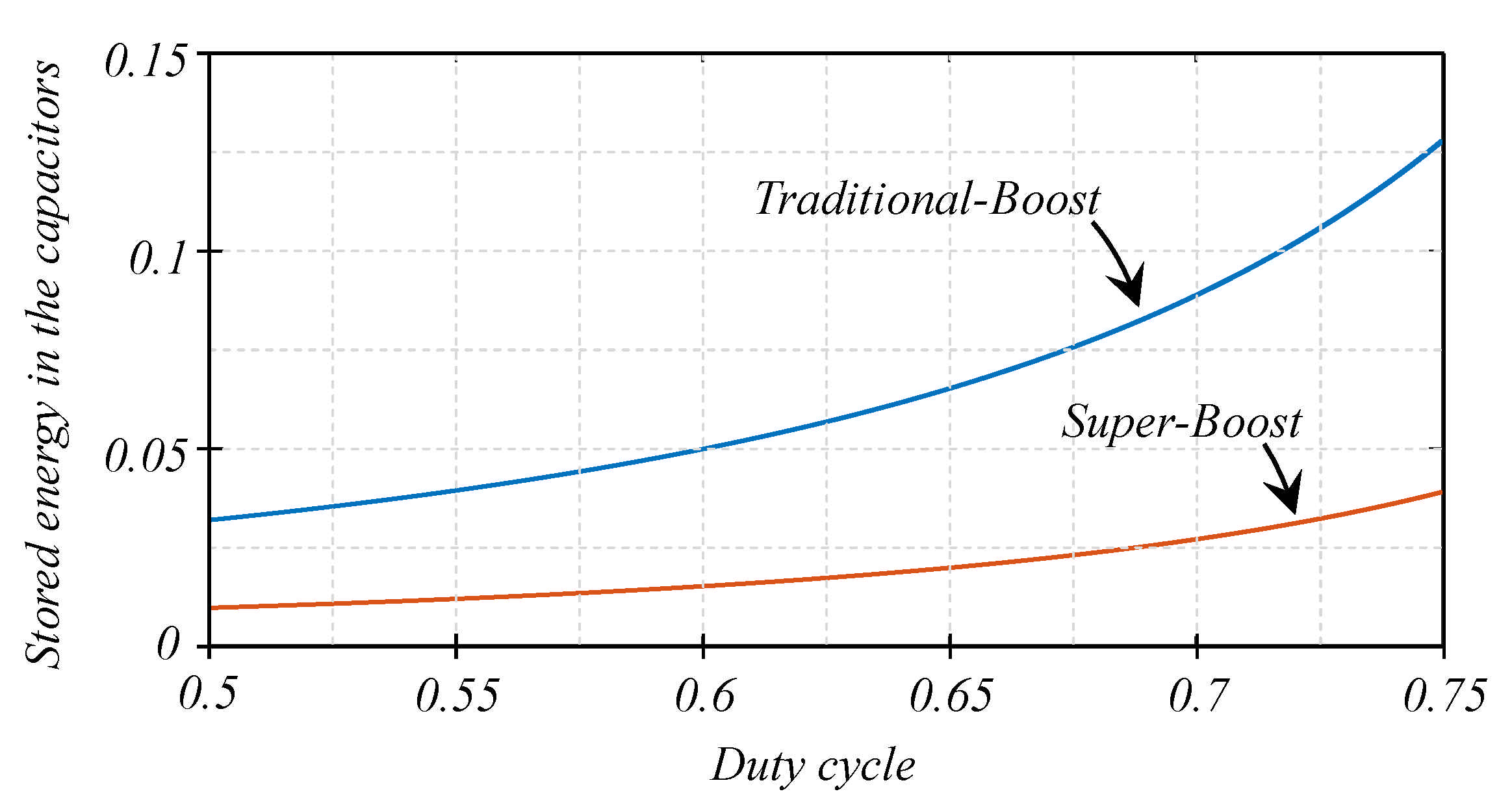
2.2. Stored Energy in Capacitors
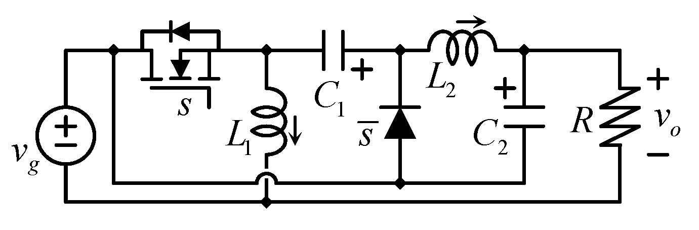
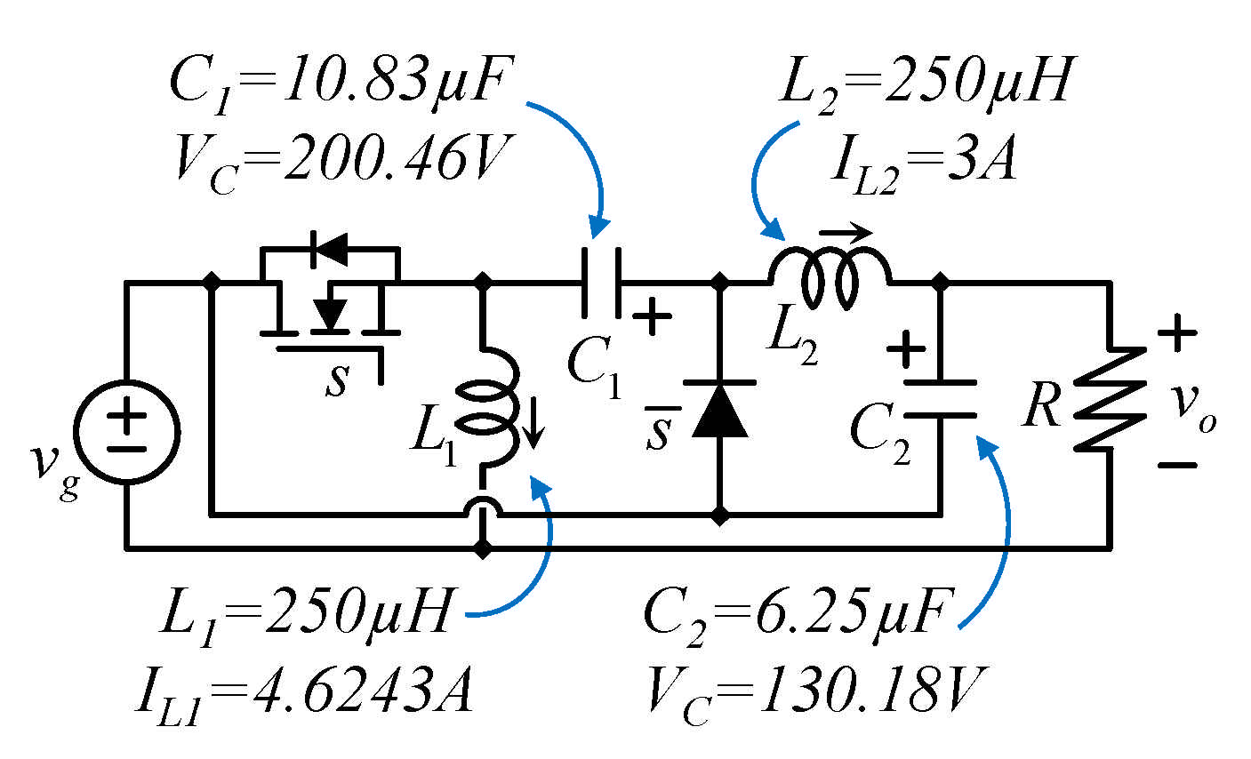
3. The Improved Super-Boost ISB (Reduced Stored Energy) Proposed Converter
3.1. Converters Mathematical Models
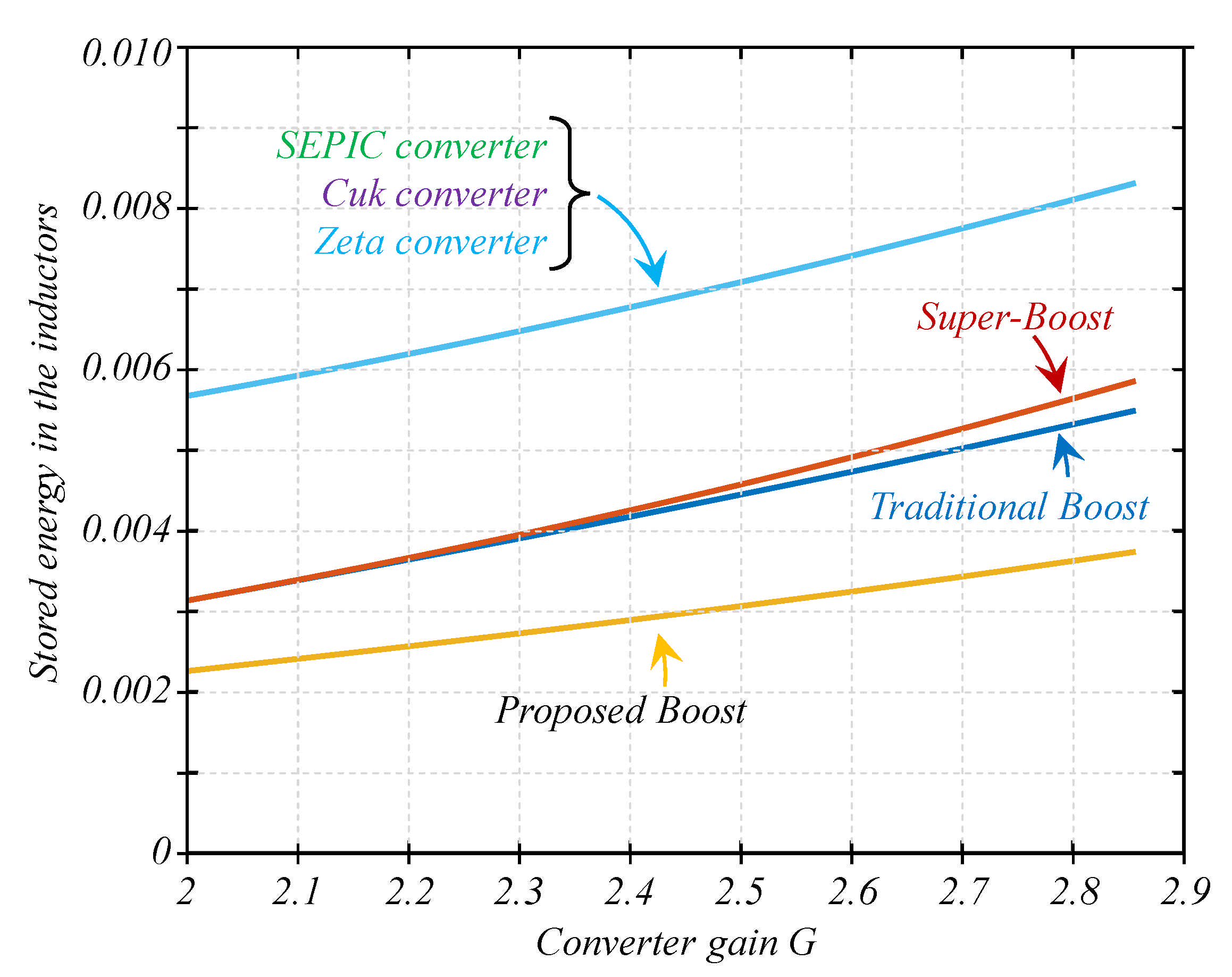
3.2. Stored Energy in Inductors
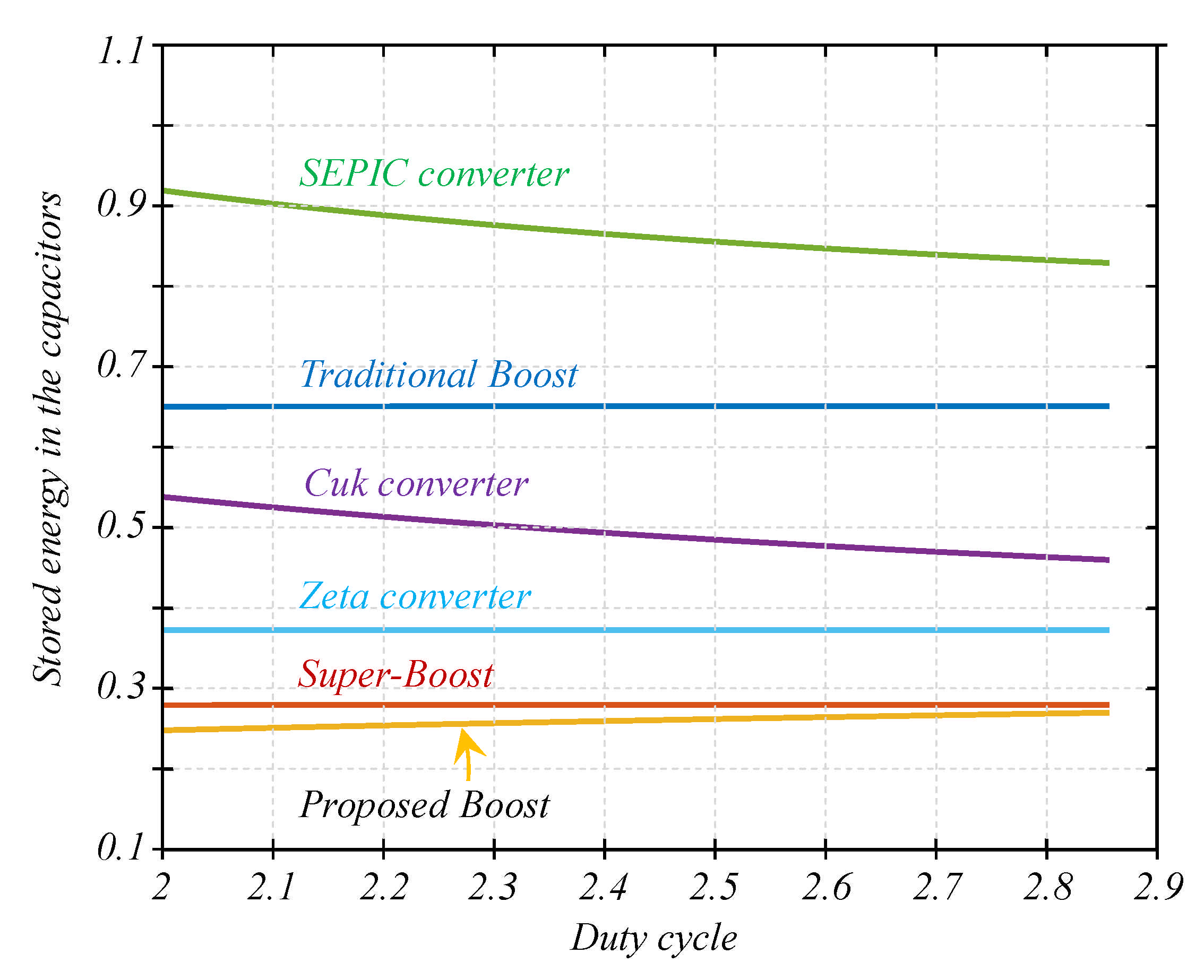
3.3. Stored Energy in Capacitors
4. Comparative Evaluation
4.1. Specifications
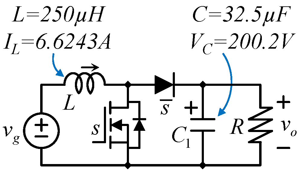
4.2. The Traditional Boost
4.3. The Super-Boost Converter
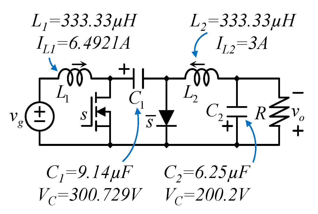
4.4. The Proposed Topology
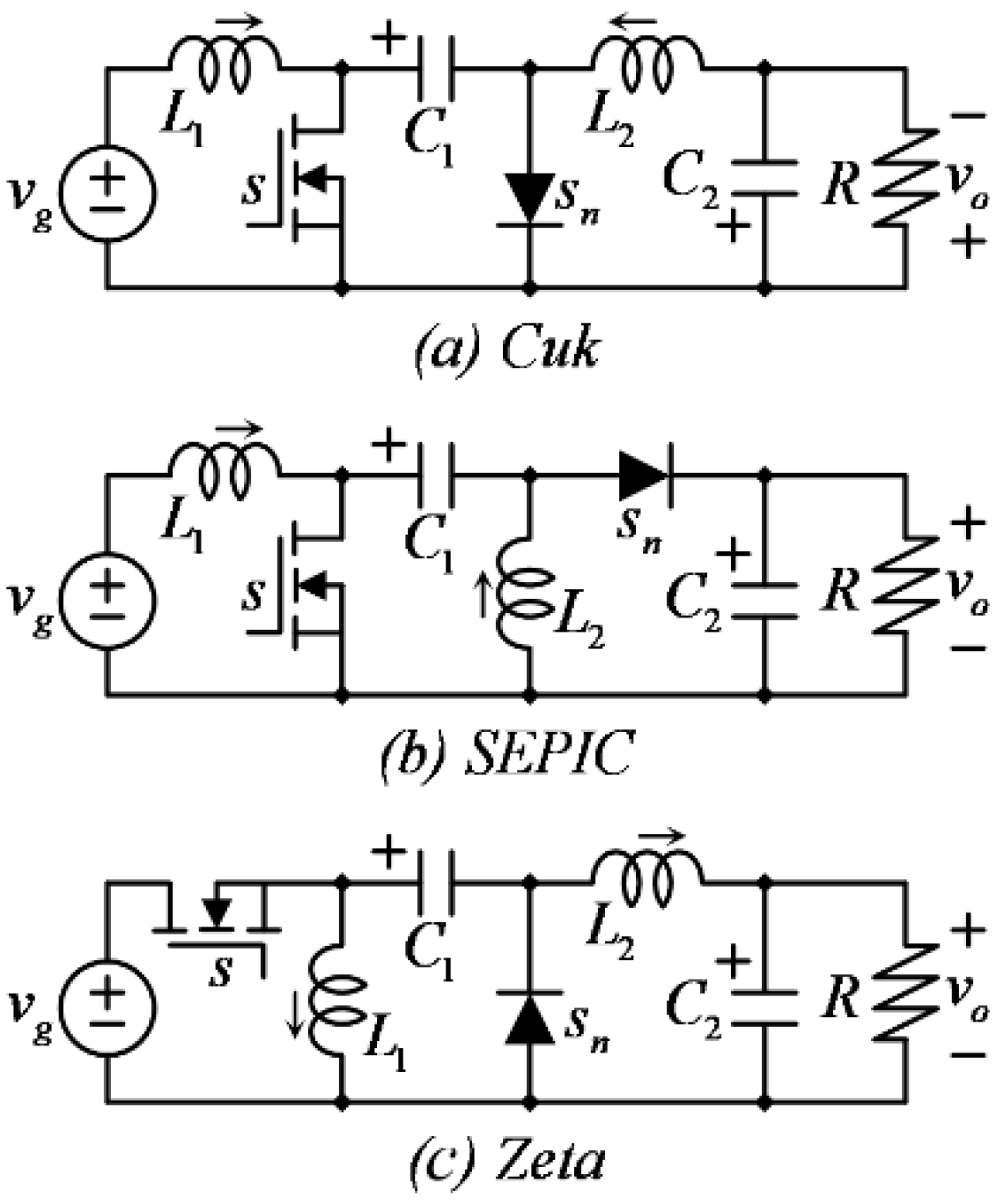
4.5. The Cuk Converter
4.6. The SEPIC Converter
4.7. The Zeta Converter
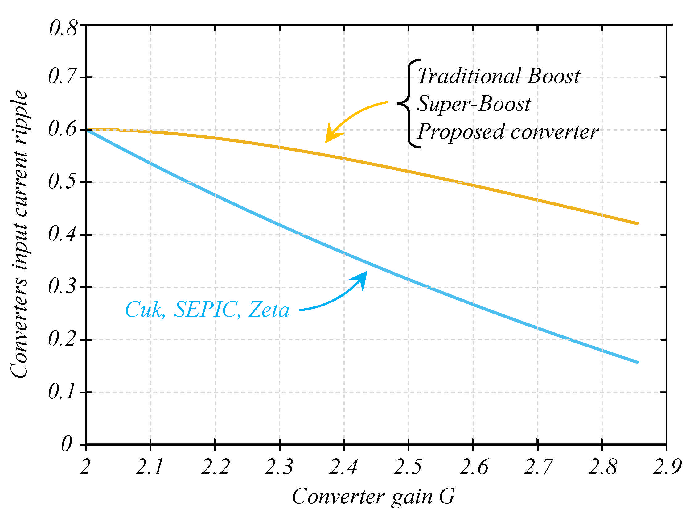
4.8. Comparison of the Converters in the Full Operating Range
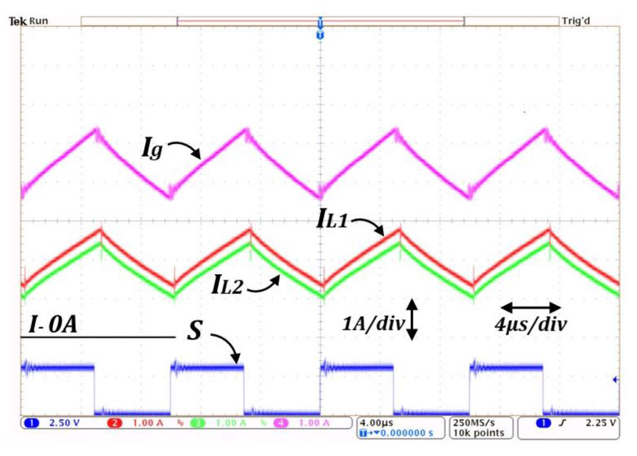
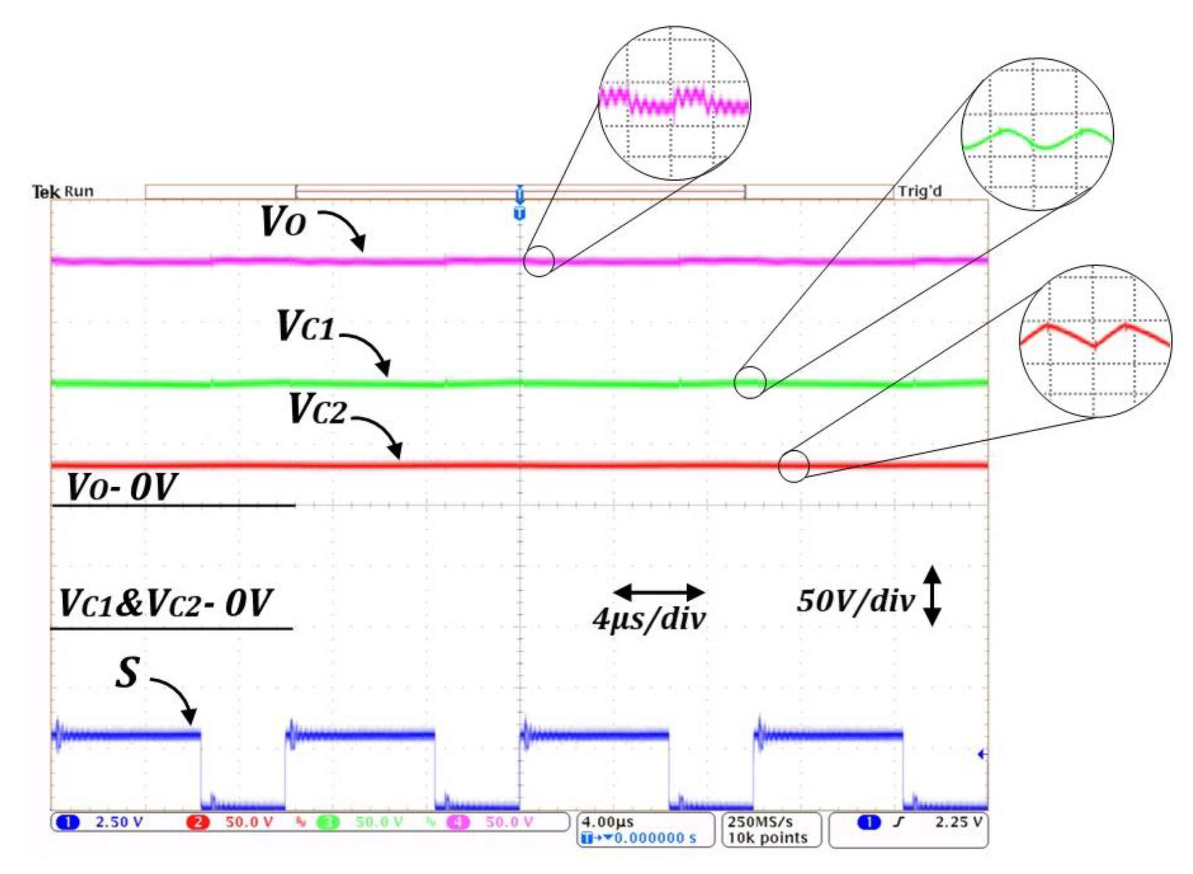
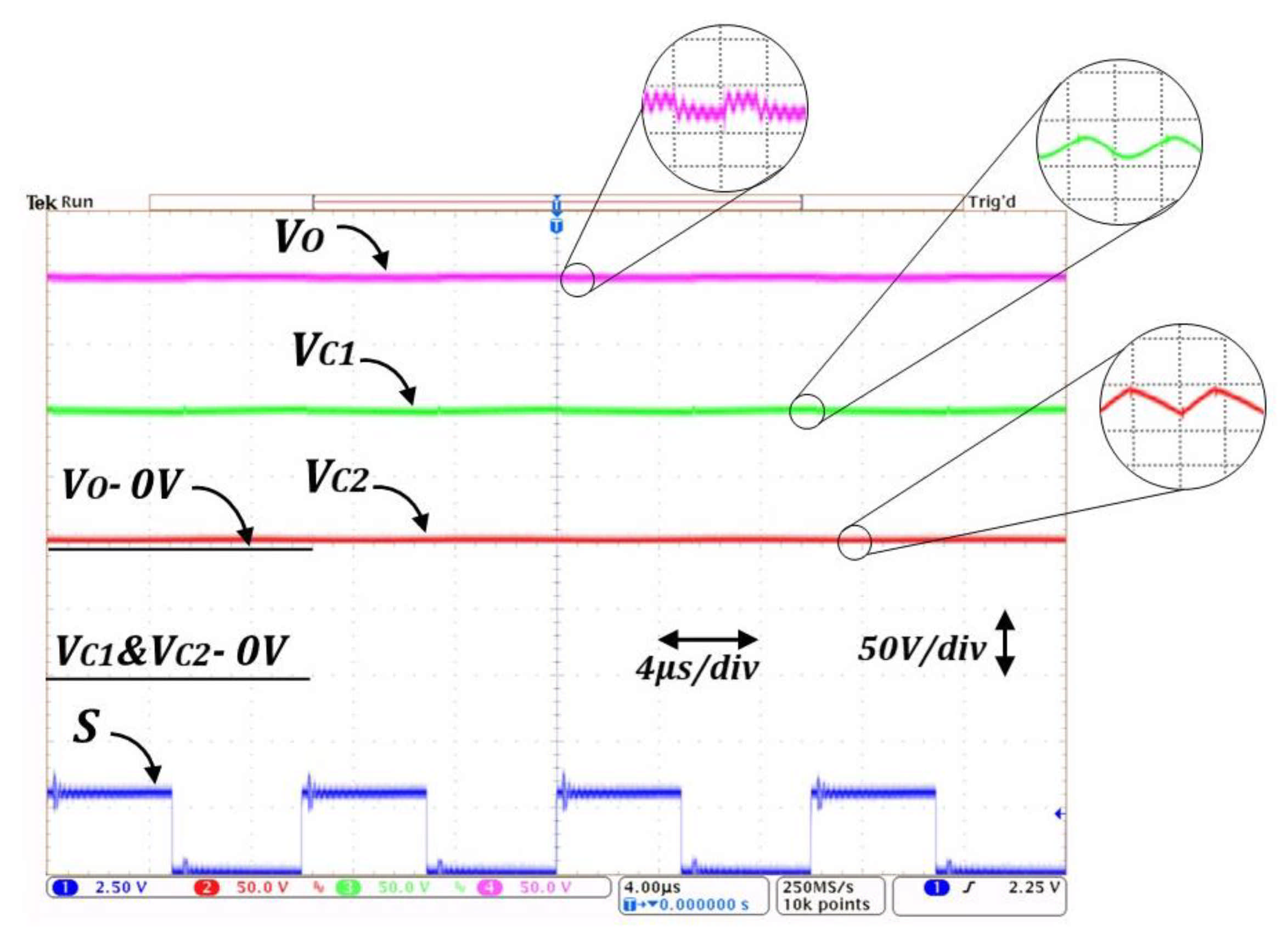
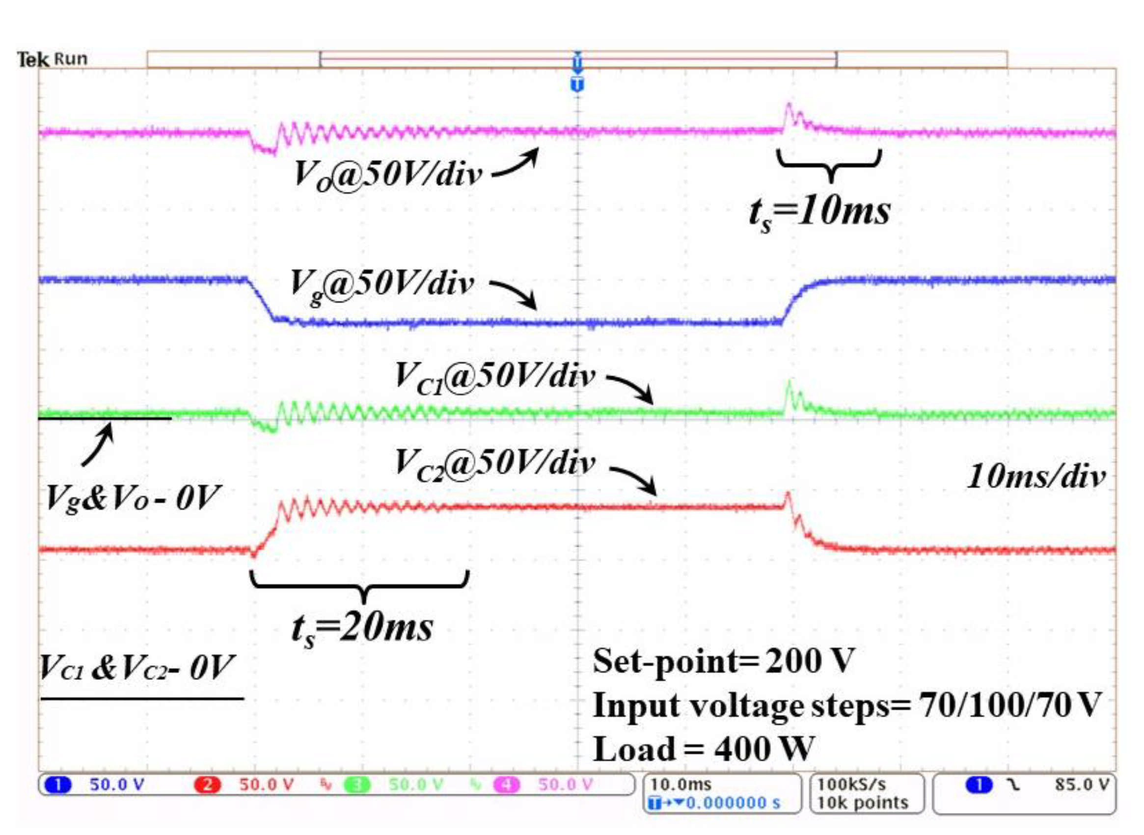
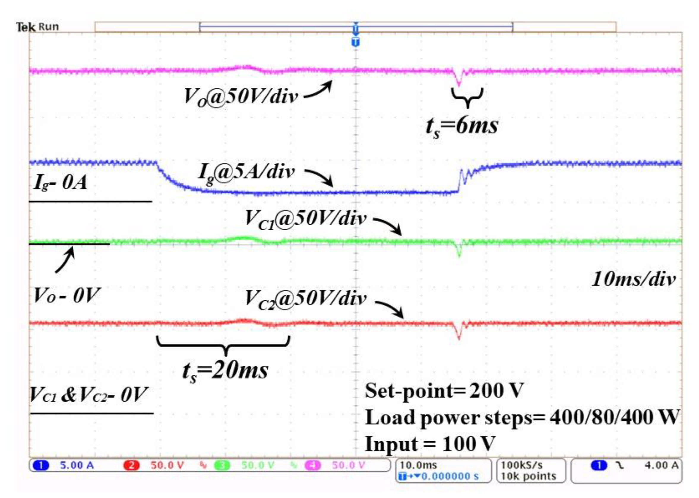
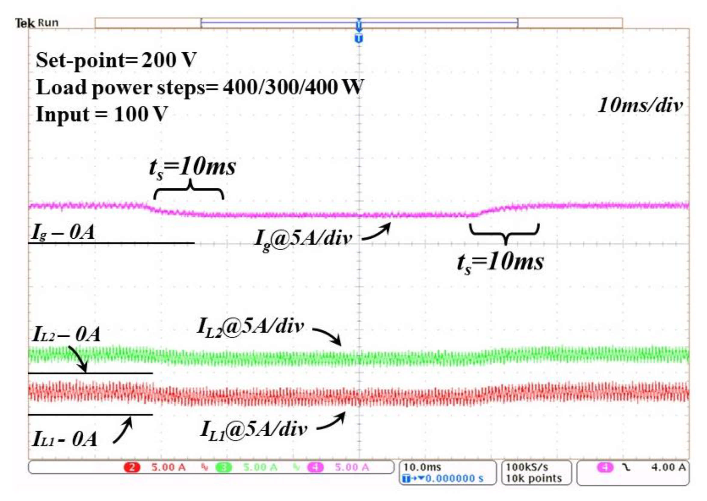
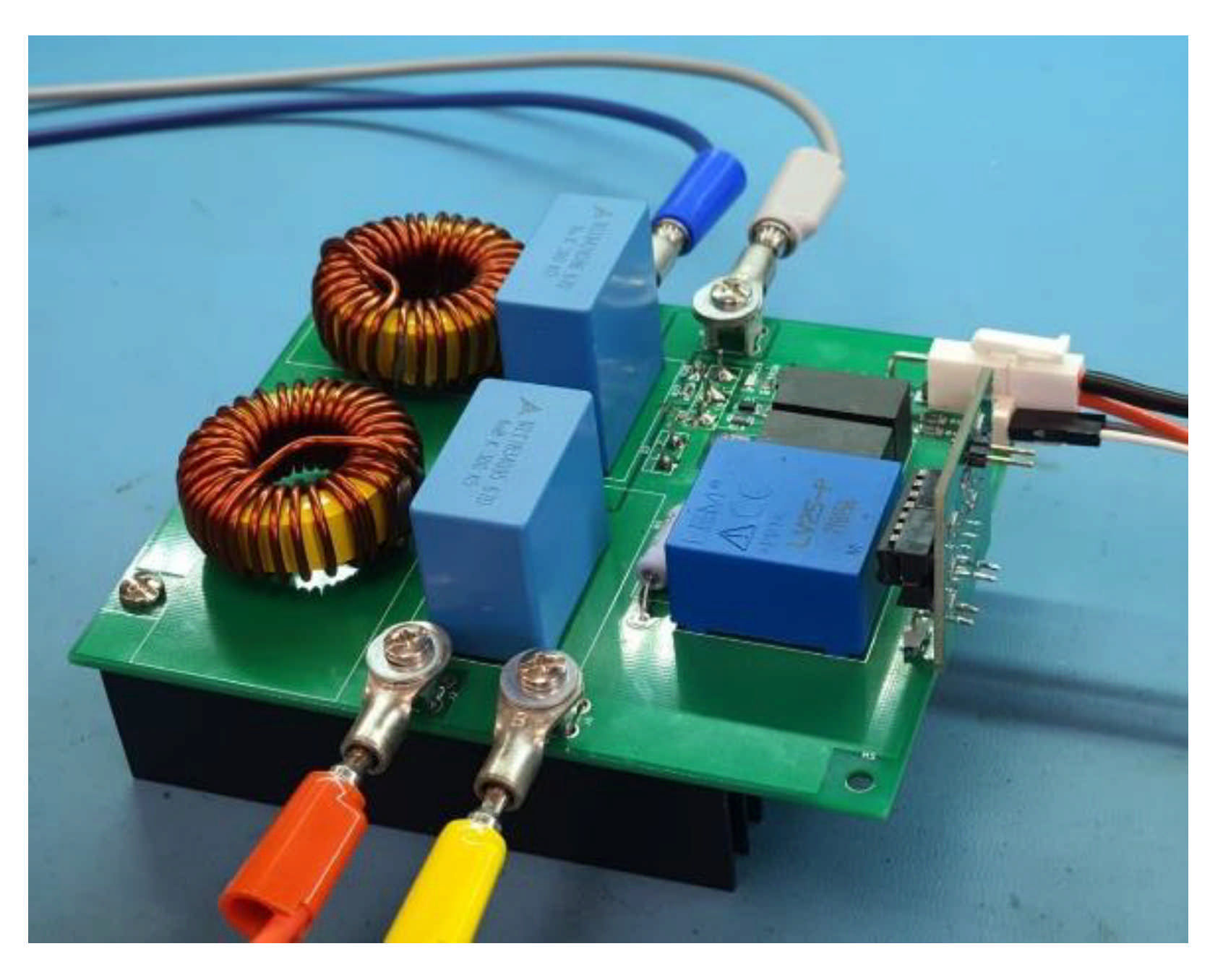
5. Experimental Results
6. Conclusions
Author Contributions
Funding
Acknowledgments
Conflicts of Interest
References
- Erickson, R.W.; Maksimovic, D. Fundamentals of Power Electronics, 2nd ed.; Kluwer: Boston, MA, USA, 2004. [Google Scholar]
- Musznicki, P.; Derkacz, P.B.; Chrzan, P.J. Wideband Modeling of DC-DC Buck Converter with GaN Transistors. Energies 2021, 14, 4430. [Google Scholar] [CrossRef]
- Bereš, M.; Kováč, D.; Vince, T.; Kováčová, I.; Molnár, J.; Tomčíková, I.; Dziak, J.; Jacko, P.; Fecko, B.; Gans, Š. Efficiency Enhancement of Non-Isolated DC-DC Interleaved Buck Converter for Renewable Energy Sources. Energies 2021, 14, 4127. [Google Scholar] [CrossRef]
- Walczak, M.; Bychto, L. Influence of Parasitic Resistances on the Input Resistance of Buck and Boost Converters in Maximum Power Point Tracking (MPPT) Systems. Electronics 2021, 10, 1464. [Google Scholar] [CrossRef]
- Rafiq, U.; Murtaza, A.F.; Sher, H.A.; Gandini, D. Design and Analysis of a Novel High-Gain DC-DC Boost Converter with Low Component Count Title. Electronics 2021, 10, 1761. [Google Scholar] [CrossRef]
- Ahmad, J.; Zaid, M.; Sarwar, A.; Lin, C.-H.; Asim, M.; Yadav, R.K.; Tariq, M.; Satpathi, K.; Alamri, B. A New High-Gain DC-DC Converter with Continuous Input Current for DC Microgrid Applications. Energies 2021, 14, 2629. [Google Scholar] [CrossRef]
- Valdez-Resendiz, J.E.; Sanchez, V.M.; Rosas-Caro, J.C.; Mayo-Maldonado, J.C.; Sierra, J.M.; Barbosa, R. Continuous input-current buck-boost DC-DC converter for PEM fuel cell applications. Int. J. Hydrog. Energy 2017, 42, 30389–30399. [Google Scholar] [CrossRef]
- Li, X.; Chen, X. A Multi-Index Feedback Linearization Control for a Buck-Boost Converter. Energies 2021, 14, 1496. [Google Scholar] [CrossRef]
- Dimitrov, B.; Hayatleh, K.; Barker, S.; Collier, G.; Sharkh, S.; Cruden, A. A Buck-Boost Transformerless DC–DC Converter Based on IGBT Modules for Fast Charge of Electric Vehicles. Electronics 2020, 9, 397. [Google Scholar] [CrossRef] [Green Version]
- Rashid, M. Power Electronics Handbook; Elsevier: Amsterdam, The Netherlands, 2011. [Google Scholar]
- Rashid, M.H. Power Electronics Handbook: Devices, Circuits and Application, 2nd ed.; Elsevier Inc.: Amsterdam, The Netherlands, 2007. [Google Scholar]
- Mohan, N. Power Electronics: A First Course, 1st ed.; John Wiley & Sons, Inc.: Hoboken, NJ, USA, 2011. [Google Scholar]
- White, J.L.; Muldoon, W.J. Two-inductor boost and buck converters. In Proceedings of the 1987 IEEE Power Electronics Specialists Conference, Blacksburg, VA, USA, 21–26 June 1987; pp. 387–392. [Google Scholar]
- Veerachary, M.; Saxena, A.R. Design of Robust Digital Stabilizing Controller for Fourth-Order Boost DC–DC Converter: A Quantitative Feedback Theory Approach. IEEE Trans. Ind. Electron. 2012, 59, 952–963. [Google Scholar] [CrossRef]
- Sammaljarvi, T.; Lakhdari, F.; Karppanen, M.; Suntio, T. Modelling and dynamic characterisation of peak-current-mode-controlled superboost converter. IET Power Electron. 2008, 1, 527–536. [Google Scholar] [CrossRef]
- Wang, B.; Tang, W. A New CUK-Based Z-Source Inverter. Electronics 2018, 7, 313. [Google Scholar] [CrossRef] [Green Version]
- Husev, O.; Shults, T.; Vinnikov, D.; Roncero-Clemente, C.; Romero-Cadaval, E.; Chub, A. Comprehensive Comparative Analysis of Impedance-Source Networks for DC and AC Application. Electronics 2019, 8, 405. [Google Scholar] [CrossRef] [Green Version]
- Ponniran, A.B.; Orikawa, K.; Itoh, J. Minimum Flying Capacitor for N-Level Capacitor DC/DC Boost Converter. IEEE Trans. Ind. Appl. 2016, 52, 3255–3266. [Google Scholar] [CrossRef]
- Lefevre, G.; Mollov, S.V. A Soft-Switched Asymmetric Flying-Capacitor Boost Converter With Synchronous Rectification. IEEE Trans. Power Electron. 2016, 31, 2200–2212. [Google Scholar] [CrossRef]
- Moradisizkoohi, H.; Elsayad, N.; Mohammed, O.A. An Integrated Interleaved Ultrahigh Step-Up DC–DC Converter Using Dual Cross-Coupled Inductors With Built-In Input Current Balancing for Electric Vehicles. IEEE J. Emerg. Sel. Top. Power Electron. 2020, 8, 644–657. [Google Scholar] [CrossRef]


| Inductor L and Capacitor C | L = 250 µH and C = 32.5 µF |
|---|---|
| Peak current in the inductor | 6.6243 A |
| Peak stored energy in the inductor | 5.5 mJ |
| Stored energy in the capacitor | 651.3 mJ |
| Inductors L1 and L2 | L1 = 500 µH, L2 = 500 µH |
|---|---|
| Capacitor C1 and C2 | C1 = 10.83 µF, C2 = 3.125 µF |
| Peak current in L1 | 4.1693 A |
| Peak current in L2 | 3 A |
| Peak stored energy in inductors | 5.9 mJ |
| Stored energy in both capacitors | 280.6 mJ |
| Inductor L1 and L2 | L1 = 250 µH, L2 = 250 µH |
|---|---|
| Capacitor C1 and C2 | C1 = 10.83 µF, C2 = 6.25 µF |
| Peak current in inductor L1 | 4.6243 A |
| Peak current in inductor L2 | 3 A |
| Peak stored energy in inductors | 3.7 mJ |
| Stored energy in capacitors | 270.9 mJ |
| Inductor L1 and L2 | L1 = 333.33 µH, L2 = 333.33 µH |
|---|---|
| Capacitor C1 and C2 | C1 = 9.14 µF, C2 = 6.25 µF |
| Peak current in inductor L1 | 6.4921 A |
| Peak current in inductor L2 | 3 A |
| Peak stored energy in inductors | 8.3 mJ |
| Stored energy in capacitors | 538.8 mJ |
| Inductor L1 and L2 | L1 = 333.33 µH, L2 = 333.33 µH |
|---|---|
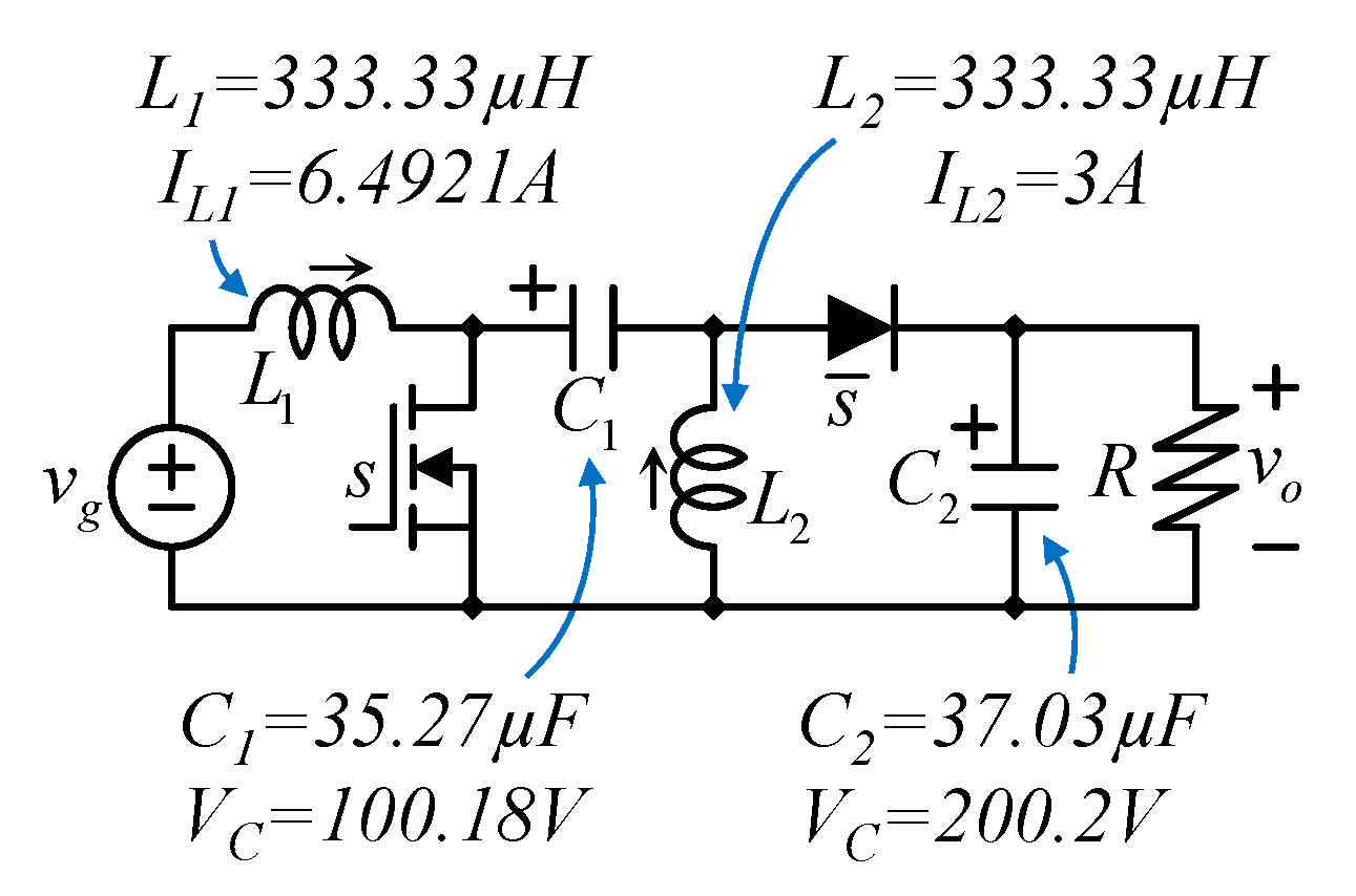
| Capacitor C1 and C2 | C1 = 35.27 µF, C2 = 37.03 µF |
| Peak current in inductor L1 | 6.4921 A |
| Peak current in inductor L2 | 3 A |
| Peak stored energy in inductors | 8.3 mJ |
| Stored energy in capacitors | 919.1 mJ |
| Inductor L1 and L2 | L1 = 333.33 µH, L2 = 333.33 µH |
|---|---|
| Capacitor C1 and C2 | C1 = 12.34 µF, C2 = 6.25 µF |
| Peak current in inductor L1 | 6.4921 A |
| Peak current in inductor L2 | 3 A |
| Peak stored energy in inductors | 8.3 mJ |
| Stored energy in capacitors | 373.6 mJ |
Publisher’s Note: MDPI stays neutral with regard to jurisdictional claims in published maps and institutional affiliations. |
© 2021 by the authors. Licensee MDPI, Basel, Switzerland. This article is an open access article distributed under the terms and conditions of the Creative Commons Attribution (CC BY) license (https://creativecommons.org/licenses/by/4.0/).
Share and Cite
Garza-Arias, E.; Rosas-Caro, J.C.; Valdez-Resendiz, J.E.; Mayo-Maldonado, J.C.; Escobar-Valderrama, G.; Guillen, D.; Rodríguez, A. The Fourth-Order Single-Switch Improved Super-Boost Converter with Reduced Input Current Ripple. Electronics 2021, 10, 2379. https://doi.org/10.3390/electronics10192379
Garza-Arias E, Rosas-Caro JC, Valdez-Resendiz JE, Mayo-Maldonado JC, Escobar-Valderrama G, Guillen D, Rodríguez A. The Fourth-Order Single-Switch Improved Super-Boost Converter with Reduced Input Current Ripple. Electronics. 2021; 10(19):2379. https://doi.org/10.3390/electronics10192379
Chicago/Turabian StyleGarza-Arias, Enrique, Julio C. Rosas-Caro, Jesus E. Valdez-Resendiz, Jonathan C. Mayo-Maldonado, Gerardo Escobar-Valderrama, Daniel Guillen, and Alma Rodríguez. 2021. "The Fourth-Order Single-Switch Improved Super-Boost Converter with Reduced Input Current Ripple" Electronics 10, no. 19: 2379. https://doi.org/10.3390/electronics10192379
APA StyleGarza-Arias, E., Rosas-Caro, J. C., Valdez-Resendiz, J. E., Mayo-Maldonado, J. C., Escobar-Valderrama, G., Guillen, D., & Rodríguez, A. (2021). The Fourth-Order Single-Switch Improved Super-Boost Converter with Reduced Input Current Ripple. Electronics, 10(19), 2379. https://doi.org/10.3390/electronics10192379