Abstract
Quasi-coherent optical receivers have recently emerged targeting access networks, offering improved sensitivity and reach over direct-detection schemes at the expense of a higher receiver bandwidth. Higher levels of system integration together with sufficiently wideband front-end blocks, and in particular high-speed linear transimpedance amplifiers (TIAs), are currently demanded to reduce cost and scale up receiver data rates. In this article, we report on the design and testing of a linear TIA enabling high-speed quasi-coherent receivers. A shunt-feedback loaded common-base topology is adopted, with gain control provided by a subsequent Gilbert cell stage. The circuit was fabricated in a commercial 130 nm SiGe BiCMOS technology and has a bandpass characteristic with a 3 dB bandwidth in the range of 5–50 GHz. A differential transimpedance gain of 68 dB was measured, with 896 of maximum differential output swing at the 1 dB compression point. System experiments in a quasi-coherent receiver demonstrate an optical receiver sensitivity of −30.5 dBm (BER = 1 × 10) at 10 Gbps, and −26 dBm (BER = 1 × 10) at 25 Gbps. The proposed TIA represents an enabling component towards highly integrated quasi-coherent receivers.
1. Introduction
Driven by new applications such as Internet-of-Things (IoT), video-on-demand, and cloud services, data traffic on the Internet continues to experience an exponential growth, with forecasts showing a continuing trend in upcoming years [1]. While datacenter networks are being progressively updated with more capable receivers and moving towards advanced modulation formats, higher demands are also being placed in the access network segment. New standards under development, including 5G, Ethernet, and NG-PON2, are seeking to maximize the yield from the deployed access infrastructures, for which an increase in data rates, reach, and number of users to be served per fiber is required. Receiver complexity and cost, however, must adapt to the price-sensitive nature of access networks, which prevents direct application of current datacenter solutions.
To tackle this challenge, low-cost receiver architectures that can offer increased performance are being explored. Among them, direct-detection receivers based on avalanche photodetectors (APDs) [2] as well as pre-amplified PIN receivers [3] have been proposed for 25 Gbps C-band links. Fiber dispersion compensation at the receiver end, however, remains a challenge, limiting the reach to about 10–15 km. While other alternatives such as Kramers–Kronig [4] or full coherent receivers allow for a longer reach, receiver cost and complexity have prevented their adoption in access networks up to this date. Coherent receivers featuring lower complexity have also been proposed for PON applications [5,6]. In [7], a simplified coherent receiver is reported achieving −37.6 dBm sensitivity (BER = 1 × 10) at 10 Gbps. A similar approach is followed in [2], reaching −35 dBm sensitivity at 25 Gbps. In both cases, however, the receiver complexity is still relatively high, requiring 3 × 3 optical couplers and three photodiodes, and resorting to offline digital signal processing (DSP).
Recently, quasi-coherent receivers have gained increased attention, offering an attractive balance between performance, cost, and receiver complexity [8]. In a quasi-coherent scheme, a local oscillator (LO) laser is used to boost receiver sensitivity, with the additional advantage of filterless wavelength division multiplexing (WDM) operation by tuning of the LO wavelength. Compensation for fiber chromatic dispersion at the receiver is also a possibility, since phase information is preserved.
A block diagram representation of a quasi-coherent receiver with polarization diversity is shown in Figure 1. The received optical signal is combined with an LO laser using an optical coupler. A polarizing beam splitter (PBS) divides the signal into orthogonal polarization components to be processed by independent receiver branches. Mixing of the received signal and LO is achieved in the photodetectors, with the resulting photocurrent expressed as [9]:
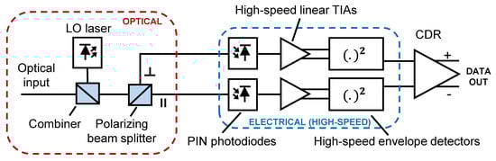
Figure 1.
Block diagram of a quasi-coherent receiver architecture with polarization diversity.
The direct-detection term and a DC component appear in the photocurrent expression, where R represents the photodetector responsivity, is the power of the received signal, and the LO power. These two terms are not required for the receiver operation and can thus be filtered out. The third term represents a bandpass intermediate frequency (IF) component, being the one processed in a quasi-coherent receiver. It contains the amplitude information of the received signal boosted by the LO laser, as well as phase information contained in and (with , and , representing, respectively, wavelength and phase for received signal and LO). For intensity-modulated transmissions, the IF takes the form of an amplitude modulated (AM) signal with carrier frequency at and two sidebands containing the transmitted data. A sufficiently wideband linear TIA is thus required to amplify this signal, which can then be demodulated by a high-speed envelope detector, avoiding in this way expensive and power-hungry digital signal processing (DSP) blocks. A clock and data recovery (CDR) circuit at the end of the receiver combines the detected signals for both polarizations.
In [10], a quasi-coherent receiver was proposed achieving a sensitivity of −35.2 dBm (BER = 1 × 10) at a 10 Gbps data rate. Polarization diversity and transmission with a standard single-mode fiber (SSMF) up to 40 km were demonstrated with negligible penalties. More recently, transmission up to 40 km was reported at 25 Gbps, with a back-to-back receiver sensitivity of −20 dBm (BER = 5 × 10) and a 6.3 dB penalty for 40 km SSMF transmission [11]. In all cases, however, system demonstrations relied on costly wideband packaged photodetectors, preventing a more practical and cost-contained system implementation. In this article, we report the design and testing of a high-speed linear TIA enabling highly integrated quasi-coherent receivers at 10 and 25 Gbps data rates. The TIA shares the same 130 nm SiGe BiCMOS platform as that of an already existing high-speed envelope detector block, aiming towards future integration of both functionalities into a single chip. A maximum differential transimpedance of 68 dB was measured, with a 3 dB response in the range of 5 to 50 GHz, and a maximum differential output swing of 896 at the 1 dB compression point. We moreover report, for the first time, a quasi-coherent receiver based on a discrete vertical PIN photodiode (PD). A receiver sensitivity of −30.5 dBm and −26 dBm (BER = 1 × 10) is demonstrated at 10 and at 25 Gbps, respectively.
The following sections review the circuit design aspects, chip measurements, and the performed system experiments evaluating the TIA performance within a quasi-coherent receiver.
2. TIA Design
Figure 2 shows a block diagram of the proposed TIA. It consists of an input high-pass filter (HPF) followed by a TIA stage, which also performs single-ended to differential conversion. A differential post-amplifier is included to provide additional gain, featuring a variable gain amplifier (VGA), a constant gain amplifier (CGA), and an output buffer. The different blocks are described in the following sections.
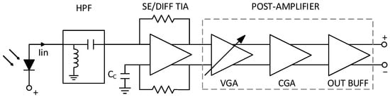
Figure 2.
Functional block diagram of the proposed TIA.
2.1. Input HPF
An HPF before the TIA serves a dual purpose. First, it sinks the DC component term in (1), which can be large due to the powerful LO laser. Additionally, it can filter out the direct-detection term, which would otherwise be present, creating distortion in the IF signal at large received powers and limiting the receiver dynamic range. A trade-off exists for the cut-off frequency of this filter. Although a high enough cut-off is desired in order to filter out the direct-detection term, this would consume a significant fraction of the available PD-TIA bandwidth for high bitrate signals. The cut-off can then be chosen at a compromised value where sufficient filtering of the direct-detection term is achieved while keeping the maximum possible available bandwidth. A second order LC filter with 5 GHz cut-off frequency was implemented, whereas additional filtering is performed in the ED block depending on the target bitrate.
In order to achieve this relatively low cut-off frequency, spiral inductors having a large inductance value are required, which in turn leads to large physical size and low self-resonance frequency (SRF). To provide a compact layout and extend the SRF, the inductors for the HPF were implemented as series inductors with opposite winding. Figure 3a shows a representation of such a dual-spiral inductor together with a typical single-spiral inductor design, both at the same scale. To compare the two approaches, an electromagnetic (EM) simulation for both designs was performed. The inductors are designed to have the same inductance value while keeping the same design parameters in both cases, that is, the same metal layer configuration, trace width, trace spacing, distance to the ground plane ring, and ground ring width. The plot in Figure 3b shows that a higher SRF can be achieved with the dual-spiral configuration for a given inductance value, while featuring a more compact layout.
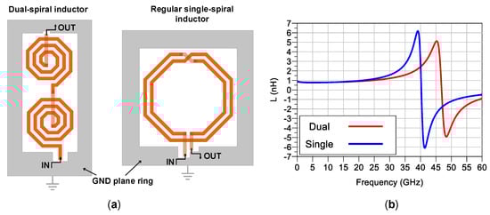
Figure 3.
Compact inductor design used in the input LC high-pass filter: (a) Comparison of dual-spiral inductor design, where two inductors with opposite winding directions are connected in series, with a regular single spiral inductor; (b) inductance as a function of frequency for the dual and single-spiral inductors obtained by electromagnetic simulation, where the self-resonance frequencies for each design are observed.
2.2. TIA Stage
Figure 4 shows a schematic of the TIA. A first common-base stage buffers the incoming photocurrent, with biasing provided by resistor at the collector node and a current mirror at the emitter. To limit power consumption and allow the largest possible bandwidth, the minimum transistor size was selected that could provide the required low TIA input impedance (below 50 ) under maximum ft biasing conditions. Double finger devices (with an emitter area of 0.12 × 0.48 µm per finger) were selected for this stage (transistors Q1–Q2) with a biasing current of around 1.4 mA per finger. The common-base is loaded by a shunt–feedback (SFB) transimpedance stage, implemented as a differential pair using single finger devices (transistors Q3–Q4), with feedback resistors and emitter degeneration and peaking provided by and . The SFB stage performs single-ended to differential conversion by AC grounding of one of its inputs through capacitor . The dummy common-base is maintained at the grounded input to provide a matched DC level, while keeping layout symmetry and suppressing additional substrate and supply noise. The values for the main circuit components are provided in the accompanying table in Figure 4.
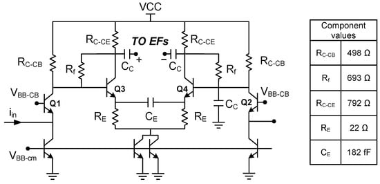
Figure 4.
Schematic of the TIA stage implementation.
The common-base stage provides a low input impedance, which is determined by transistor sizing and current, and thus is not dependent on the feedback resistor . This helps with speeding up the input node of the TIA in the presence of a relatively large photodetector capacitance. The gain-bandwidth trade-off affecting the SFB topology is now effectively decoupled from the photodetector, and limited now by circuit and technology constraints. As a known drawback, this topology usually features higher noise and power consumption compared to a classical SFB TIA [12]. Although further noise optimization of this stage is possible [13], this was not prioritized in this design. Additional LO laser power can be used instead to push the receiver sensitivity towards the shot-noise limit.
2.3. Post-Amplifier
A post-amplifier is used to provide additional voltage gain after the TIA stage. First, the inter-stage buffer circuit shown in Figure 5 is used to sense the TIA output voltage and drive the following VGA block. The buffer consists of DC coupled cascaded emitter followers, simultaneously realizing high input impedance and low output impedance, both desirable properties for voltage buffering. The first pair (Q1–Q2) makes use of single finger devices to lower the capacitive loading to the preceding stage, while being able to drive the larger capacitance of the subsequent pair (Q3–Q4) implemented with three finger devices, having a higher driving capability towards the following stages. Current sources at the emitter nodes are realized with a cascoded current mirror at the first EF pair (same sizing as Q1–Q2), while a regular current mirror is used in the second pair (same sizing as Q3–Q4). Additional voltage is dropped by a diode at the collector node of the second pair for proper headroom allocation. All transistors are biased at 1.4 mA per finger. The circuit is subsequently used between the VGA and CGA stages in the post-amplifier. Additionally, it is also used as an output buffer, since it features the optimal driving characteristics towards the envelope detector following the TIA.
Figure 5.
Schematic of the cascaded emitter followers used as an inter-stage buffer. The same stage is also used as an output buffer for the complete circuit.
Figure 6 shows the schematic circuit for the VGA and CGA stages. The VGA, represented in Figure 6a, is implemented as a Gilbert cell, where the offset voltage for the center transistor pair in the switching quad (transistors Q5–Q6) is used to control the gain. Emitter degeneration in the bottom transistor pair (Q1–Q2) is used to linearize the response while providing increased input impedance. Values for the collector resistor RC and emitter resistor RE are 174 and 35 , respectively. The tail current source for the bottom pair is implemented with a current mirror providing bias current of 1.4 mA per finger to the active devices (Q1–Q4 when Q5–Q6 are switched off), with all transistors in the stage being two finger devices. The CGA, shown in Figure 6b, follows the same topology, where the center transistor pair from the switching quad is simply removed, leaving out a standard cascode amplifier. Due to both stages featuring a high output impedance, and together with the high input impedance of the inter-stage EF buffers, the top collector for both stages remains a high impedance node. The relatively small parasitic capacitance contributions from the different components, as well as the associated layout interconnects, can thus impose significant bandwidth limitations at this node. To compensate for this effect, shunt inductive peaking is used at the top collector nodes in both stages, provided by inductor LC with an inductance value of 0.22 nH obtained from EM simulation. This helps with speeding up the critical nodes, effectively overcoming the bandwidth limitations. As can be observed in the different subcircuit schematics, AC coupling is used at different nodes throughout the circuit. The use of AC coupling, enabled by the bandpass characteristic of the TIA, is preferred since it can provide additional voltage headroom clearance while avoiding the need for DC offset cancellation circuitry.
Figure 6.
Schematic representation for: (a) Gilbert-cell-based VGA with emitter degeneration and shunt inductive peaking; (b) CGA formed by a cascode gain stage with emitter degeneration and shunt inductive peaking.
3. Measurement Results and Discussion
This section presents the measurement results for the fabricated TIA chip. In the first subsection, RF probing measurements are provided and discussed. The following subsection reports system experiments conducted around a quasi-coherent receiver featuring the proposed TIA.
3.1. On-Wafer Characterization
First, small signal performance of the chip was evaluated by on-wafer measurements using a 2-port vector network analyzer (VNA). All measurements were performed with a supply voltage of 3.3 V, with the circuit drawing around 69 mA for a total DC power consumption of around 228 mW. The output power from the VNA was set to −40 dBm to ensure linear operation at maximum gain. Figure 7a shows the measured forward S-parameters for each of the differential TIA outputs ( and ). In each case, the unused TIA output is DC blocked and terminated in a 50 load. The differential transimpedance response was obtained from the measured S-parameters, and is plotted in the figure together with the simulated response. For the simulated transimpedance, RC parasitic extraction of the amplifier core was combined with electromagnetic simulation of input and output structures and peaking inductors. Excellent agreement between measurement and simulation is observed. Lower and higher 3 dB cut-off frequencies (measured relative to the maximum transimpedance value of 68 dB) of 5 and 50 GHz, respectively, are obtained using a moving average (1 GHz wide) on the measured data. This was done in order to better illustrate the amplifier response towards the higher frequency end, where setup limitations lead to excess noise in the measurements. Figure 7b shows the behavior of the gain control functionality in the S-parameter response for one of the TIA outputs, where the possibility for gain reduction down to around 0 dB is demonstrated.
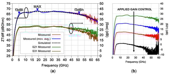
Figure 7.
Small signal TIA measurements: (a) measured S-parameters (where and correspond to the forward transmission coefficients from the input port to each of the differential TIA outputs, cf. Figure 2) and transimpedance response calculated from measurements, compared to simulation results; (b) effect of the gain control functionality on the S-parameter response for one of the TIA outputs.
Figure 8a shows the simulated and measured group delay response. A moving average (2 GHz wide) was applied to the measurements to better illustrate the trend. The measured group delay variation closely follows the trend of the simulated response up to 35 GHz. Above this value, larger deviations are observed from the simulations. Figure 8b shows the amplitude and phase imbalance between the two TIA outputs. Good agreement is obtained for the phase imbalance up to 35 GHz. Above this frequency, the measured response also deviates from the simulation. This deviation from the simulated response in the phase measurements was mainly attributed to the limited accuracy of the setup, where excessive noise due the low input power used in the measurements can compromise the highly sensitive phase response. The amplitude imbalance remains within ±1 dB up to 45 GHz. A 0.5 dB difference between the two outputs is observed already at low frequencies, which falls within the repeatability of the measurements, since the two outputs must be measured independently using a 2-port VNA.
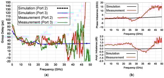
Figure 8.
Small signal TIA measurements: (a) simulated and measured group delay response for each of the differential TIA outputs (ports 2 and 3); (b) amplitude and phase imbalance (deviation from out-of-phase condition) between the two TIA outputs.
To evaluate the large signal performance, the 1 dB compression of the circuit was measured at 15 and 20 GHz. The probed circuit was fed from a signal generator, while the output power was monitored in a spectrum analyzer. Losses from cables and probes in the setup were calibrated out by probing of a thru standard from a calibration substrate. Figure 9 shows the resulting curves, where linear fits are provided for reference, together with markers identifying the 1 dB compression points. For both frequencies, the 1 dB compression is found at an input power of −30 dBm, with a corresponding output power around −3 dBm. In the figure, the simulated response is also provided. Slightly higher gain values are obtained in this case, since the circuit model for large signal simulation includes only parasitic capacitance extraction. The compression point, however, occurs at a similar output power. From the measured response, a differential output swing of 896 is obtained at 1 dB compression. This large output swing is facilitated by the use of emitter followers as output buffers, where the output swing is determined by device linearity and not constrained by power consumption, as would be the case for a 50 matched common emitter stage.
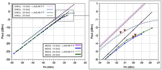
Figure 9.
Measured and simulated 1 dB compression point at 15 and 20 GHz. Linear fits are provided together with markers identifying the 1 dB compression. The magnified view on the right side provides a detailed view around the 1 dB compression points.
3.2. System Experiments
The performance of the proposed TIA was also verified within a quasi-coherent receiver setup. In order to simplify testings, a single-polarization receiver was implemented as shown in Figure 10. An externally modulated laser (EML) is used as a transmitter, followed by a variable optical attenuator (VOA) that controls the optical power entering the receiver (). The received signal is combined with a local oscillator laser by means of an optical coupler. After the coupler, a polarization beam splitter (PBS) separates the combined signal into orthogonal polarizations. The LO is an external cavity laser (ECL) with a linewidth of 100 kHz and an emitted power of 14 dBm (). By means of polarization controllers, the LO polarization is aligned to obtain 50% of the power at each output of the PBS, while the signal polarization is fully aligned to the PBS output being measured. This allows for more accurately relating the obtained system performance to that of a complete receiver implementing polarization diversity, since half of the available LO power is in this case left out, which would be required for the second polarization. The combined LO and signal from the PBS output in use are then focused into a lensed PIN photodiode using a focusing lens. The photodiode has a specified responsivity of 0.8 A/W at 1310 nm (expected to be reduced at 1550 nm) and an opto-electrical (O/E) bandwidth of 37 GHz. The resulting photocurrent is then amplified with the designed TIA and downconverted to baseband with a high-speed envelope detector (ED). Finally, the recovered baseband signal is amplified with a commercial limiting amplifier and processed in a bit-error-rate testset (BERT). The complete chip sub-assembly including PD, TIA, and ED is mounted on an evaluation board as shown in Figure 11, where the individual dies are interconnected by wirebonding. A magnified view of the die sub-assembly is provided in the figure, where the different blocks are identified. The designed TIA chip has dimensions of 0.72 mm × 1.1 mm for a total area of around 0.79 mm2.
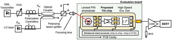
Figure 10.
Single-polarization receiver setup used to evaluate the TIA performance.
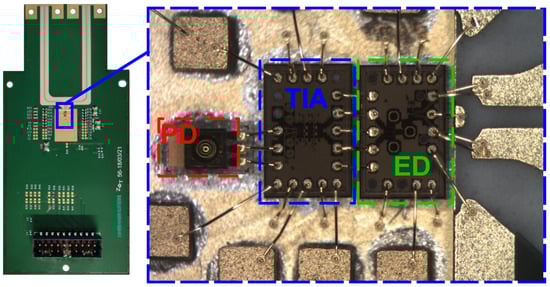
Figure 11.
Evaluation board hosting the electrical receiver front-end (left) with magnified view of the die sub-mount consisting of a lensed PIN photodetector, the fabricated TIA chip, and a high-speed envelope detector. Both TIA and ED chips have been fabricated in the same technology.
First, measurements to estimate the opto-electrical 3 dB bandwidth of the complete receiver were carried out. Since an envelope detector is present in the receiver, the test is performed by transmitting a narrowband signal consisting of 3 Gbps non-return-to-zero (NRZ) data (minimum bitrate accepted by the EML transmitter). The LO wavelength is then swept, shifting the IF center frequency accordingly, and the output signal from the detector is monitored in a sampling oscilloscope. The curve in Figure 12 shows the detected power as a function of IF center frequency, with a 3 dB response in the range of 16 to 37 GHz. In the figure, the simulated response is also provided. An inset shows the simulation setup, for which the measured TIA response has been used together with a post-layout simulation of the envelope detector. The simulated response includes a photodetector model with associated parasitics, as well as wirebond interconnects modeled as pure inductances. The values for the parasitic capacitance C and series resistance R represent averaged values taken from measured data provided by the manufacturer for the particular chip lot used in the system setup. The wirebond inductance was adjusted in simulation since its actual value cannot be accurately estimated. Using a wirebond inductance of 0.1 nH, good agreement is obtained between measurement and simulation, with a response affected by the bandwidth limiting parasitics from both the photodetector and the chip-to-chip interconnects (pad capacitances and wirebond inductances). An additional HPF with 12 GHz cut-off is implemented in the envelope detector for optimal performance at 25 Gbps bitrates, which shifts the overall lower cut-off to higher frequencies. Further integration of TIA and envelope detector into a single chip is expected to provide improved performance.
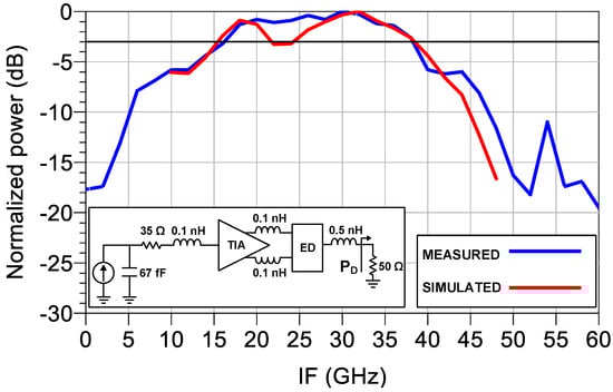
Figure 12.
Measured and simulated opto-electrical bandwidth of the receiver using a 3 Gbps NRZ data transmission with swept IF center frequency. The inset shows a schematic representation of the simulation setup.
Measurements for the optical receiver sensitivity are reported in Figure 13, with marked lines representing the NG-PON2 forward error correction (FEC) limit (BER = 1 × 10) and the Ethernet FEC limit (BER = 5 × 10). The measurements were performed at 10 and 25 Gbps data rates. For the 10 Gbps case, an EML transmitter was used having an extinction ratio (ER) of 15.28 dB, emitted power of 0.44 dBm, and center wavelength at 1548.75 nm. In turn, the 25 Gbps signal was generated with an EML having an ER of 9.3 dB, emitted power of 2.9 dBm and center wavelength at 1561.48 nm. A sensitivity of −30.5 dBm for the NG-PON2 FEC limit and −28.5 dBm for the Ethernet FEC limit is obtained at 10 Gbps. The 25 Gbps BER curve shows an error floor around 1 × 10, which was attributed to insufficient O/E bandwidth in the receiver. Nevertheless, the receiver can still perform below the FEC limits, achieving −26 and −23 dBm sensitivity for NG-PON2 and Ethernet FEC limits, respectively, thereby improving by 3 dB the results obtained in [11] at 25 Gbps back-to-back.
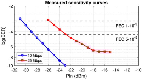
Figure 13.
Measured BER as a function or received optical power () at 10 and 25 Gbps data rates. Line markers indicate the NG-PON2 and Ethernet FEC limits at BER = 1 × 10 and BER = 5 × 10, respectively.
To conclude, Table 1 summarizes the main parameters obtained from the TIA characterization against the relevant state-of-the-art. The reported TIA shows an overall good performance, enabling a high receiver sensitivity in a quasi-coherent receiver setup.

Table 1.
Comparison of the proposed TIA against the state-of-the-art.
4. Conclusions
The design and testing of a high-speed linear TIA targeting quasi-coherent receivers have been presented and discussed in detail. Circuit measurements have shown a 3 dB response in the range of 5 to 50 GHz, with a differential transimpedance of 68 dB and a maximum differential output swing of 896 at 1 dB compression. A quasi-coherent receiver based on a discrete vertical PIN photodiode and featuring the designed TIA has been introduced, achieving a receiver sensitivity of −30.5 dBm and −26 dBm (BER = 1 × 10) at 10 and at 25 Gbps, respectively. The proposed TIA has thus proven an enabling block towards highly integrated quasi-coherent receivers operating at high speeds.
Author Contributions
Conceptualization, G.S.V., J.B.J. and T.K.J.; methodology, G.S.V., J.B.J. and T.K.J.; resources, J.B.J. and T.K.J.; measurements and experimental results, G.S.V., M.K. and T.K.J.; writing—original draft preparation, G.S.V., J.A.A.; writing—review and editing, G.S.V., J.A.A. and T.K.J.; supervision, J.B.J. and T.K.J.; project administration, J.B.J. and T.K.J.; funding acquisition, J.B.J. and T.K.J. All authors have read and agreed to the published version of the manuscript.
Funding
This research was supported by the INCOM project (ID: 8057-00059B), partly funded by Innovation Fund Denmark.
Acknowledgments
The authors would like to acknowledge Omar Gallardo Puertas for PCB mounting and additional support with the measurements.
Conflicts of Interest
The authors declare no conflict of interest. The funders had no role in the design of the study; in the collection, analyses, or interpretation of data, and in the writing of the manuscript or in the decision to publish the results.
References
- Cisco Annual Internet Report (2018–2023) White Paper. 2020. Available online: https://www.cisco.com (accessed on 1 July 2021).
- Houtsma, V.; van Veen, D. Bi-Directional 25G/50G TDM-PON With Extended Power Budget Using 25G APD and Coherent Detection. J. Light. Technol. 2018, 36, 122–127. [Google Scholar] [CrossRef]
- Borkowski, R.; Poehlmann, W.; Brenot, R.; Bonk, R.; Angelini, P.; Caillaud, C.; Achouche, M.; Blache, F.; Goix, M.; Mekhazni, K.; et al. Real-time burst-mode operation of an integrated SOA-PIN/TIA receiver for 25 Gbit/s/λ and faster T(W)DM-PON. In Proceedings of the Optical Fiber Communications Conference and Exhibition (OFC), Los Angeles, CA, USA, 19–23 March 2017; pp. 1–3. [Google Scholar]
- Mecozzi, A.; Antonelli, A.; Shtaif, M. Kramers–Kronig receivers. Adv. Opt. Photon. 2019, 11, 480–517. [Google Scholar] [CrossRef]
- Erkılınc, M.S.; Lavery, D.; Shi, K.; Thomsen, B.C.; Killey, R.I.; Savory, S.J.; Bayvel, P. Comparison of Low Complexity Coherent Receivers for UDWDM-PONs ( λ-to-the-User). J. Light. Technol. 2018, 36, 3453–3464. [Google Scholar] [CrossRef]
- Teixeira, A.; Lavery, D.; Ciaramella, E.; Schmalen, L.; Iiyama, N.; Ferreira, R.M.; Randel, S. DSP Enabled Optical Detection Techniques for PON. J. Light. Technol. 2020, 38, 684–695. [Google Scholar] [CrossRef]
- Rannello, M.; Presi, M.; Ciaramella, E. PBS-Free Polarization-Independent PON Coherent Receiver. IEEE Photonics Technol. Lett. 2020, 32, 1361–1364. [Google Scholar] [CrossRef]
- Jensen, J.B.; Altabas, J.A.; Gallardo, O.; Squartecchia, M.; Valdecasa, G.S. Quasi-coherent Technology for Cost Efficient High Loss Budget Transmission. In Proceedings of the Optical Fiber Communications Conference and Exhibition (OFC), San Diego, CA, USA, 8–12 March 2020; pp. 1–3. [Google Scholar]
- Agrawal, G. Fiber-Optic Communication Systems; Wiley Series in Microwave and Optical Engineering; Wiley: Hoboken, NJ, USA, 2012. [Google Scholar]
- Altabas, J.A.; Valdecasa, G.S.; Suhr, L.F.; Didriksen, M.; Lazaro, J.A.; Garces, I.; Monroy, I.T.; Clausen, A.T.; Jensen, J.B. Real-Time 10 Gbps Polarization Independent Quasicoherent Receiver for NG-PON2 Access Networks. J. Light. Technol. 2019, 37, 651–656. [Google Scholar] [CrossRef] [Green Version]
- Altabas, J.A.; Gallardo, O.; Valdecasa, G.S.; Squartecchia, M.; Johansen, T.K.; Jensen, J.B. DSP-Free Real-Time 25 GBPS Quasicoherent Receiver With Electrical SSB Filtering for C-Band Links up to 40 km SSMF. J. Light. Technol. 2020, 38, 1785–1788. [Google Scholar] [CrossRef]
- Säckinger, E. Analysis and Design of Transimpedance Amplifiers for Optical Receivers; Wiley: Hoboken, NJ, USA, 2017. [Google Scholar]
- Vanisri, T.; Toumazou, C. Integrated high frequency low-noise current-mode optical transimpedance preamplifiers: Theory and practice. IEEE J.-Solid-State Circuits 1995, 30, 677–685. [Google Scholar] [CrossRef]
- Awny, A.; Nagulapalli, R.; Winzer, G.; Kroh, M.; Micusik, D.; Lischke, S.; Knoll, D.; Fischer, G.; Kissinger, D.; Ulusoy, A.C.; et al. A 40 Gb/s Monolithically Integrated Linear Photonic Receiver in a 0.25μm BiCMOS SiGe:C Technology. IEEE Microw. Wirel. Components Lett. 2015, 25, 469–471. [Google Scholar] [CrossRef]
- A wideband monolithically integrated photonic receiver in 0.25-µm SiGe:C BiCMOS technology. In Proceedings of the ESSCIRC Conference 2016: 42nd European Solid-State Circuits Conference, Lausanne, Switzerland, 12–15 September 2016; pp. 487–490. [CrossRef]
- Andrade, H.; Hirokawa, T.; Maharry, A.; Rylyakov, A.; Schow, C.L.; Buckwalter, J.F. Monolithically-Integrated 50 Gbps 2pJ/bit Photoreceiver with Cherry-Hooper TIA in 250 nm BiCMOS Technology. In Proceedings of the Optical Fiber Communications Conference and Exhibition (OFC), San Diego, CA, USA, 3–7 March 2019; pp. 1–3. [Google Scholar]
- García López, I.; Awny, A.; Rito, P.; Ko, M.; Ulusoy, A.C.; Kissinger, D. 100 Gb/s Differential Linear TIAs With Less Than 10 pA/ in 130-nm SiGe:C BiCMOS. IEEE J.-Solid-State Circuits 2018, 53, 458–469. [Google Scholar] [CrossRef]
- Khafaji, M.M.; Belfiore, G.; Ellinger, F. A Linear 65-GHz Bandwidth and 71-dBΩ Gain TIA With 7.2 pA/ in 130-nm SiGe BiCMOS. IEEE-Solid-State Circuits Lett. 2021, 4, 76–79. [Google Scholar] [CrossRef]
Publisher’s Note: MDPI stays neutral with regard to jurisdictional claims in published maps and institutional affiliations. |
© 2021 by the authors. Licensee MDPI, Basel, Switzerland. This article is an open access article distributed under the terms and conditions of the Creative Commons Attribution (CC BY) license (https://creativecommons.org/licenses/by/4.0/).