
Asymmetric Doherty Power Amplifier with Input Phase/Power Adjustment and Envelope Tracking


Abstract
:1. Introduction
2. Doherty Amplifier Design
2.1. Asymmetrical DPA Theory
2.2. Class-F Main PA Design
- Firstly, the open stubs (Line9 and Line7) are utilized in order to realize the second harmonic impedance short circuited and the third harmonic impedance open circuited, which are the harmonic suppression requirements of a third order Class-F mode PA, as shown in Figure 2b;
- Secondly, the fundamental matching for the optimum output power is designed as Ropt = 33 Ohm from the Igen plane;
- Finally, the output impedance at the Igen plane is also inverse to the load fundamental impedance in order to keep the maximum voltage sweep range and the maximum efficiency at the power back-off condition. This is the key part for the load-pull function to the main PA. With the variation of , the impedance is seen from the Igen plane at , and Z1, is inversed to the . As shown in Figure 2b, as shifts from 30 Ohm to 15 Ohm, Real (Z1) @ changes from 33 Ohm to 64 Ohm, while the second harmonic impedance is kept in the nearly short condition (Real (Z1) @ 2 = 4 Ohm) during the load-pull process, and the third harmonic impedance is fixed to be closed to the open condition (Real (Z1) @ 3 = 830 Ohm).
2.3. Class-C Auxiliary PA Design
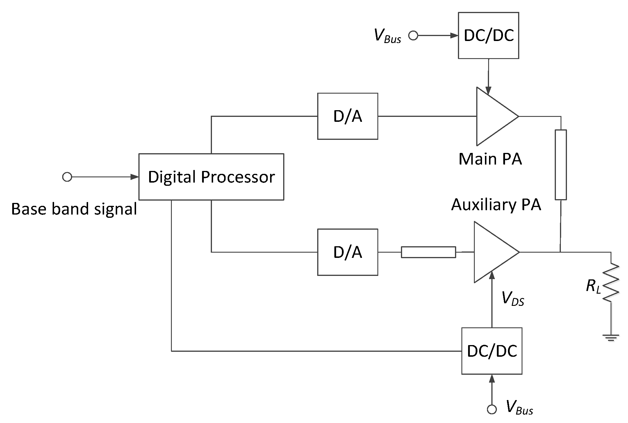
2.4. Doherty PA Realization
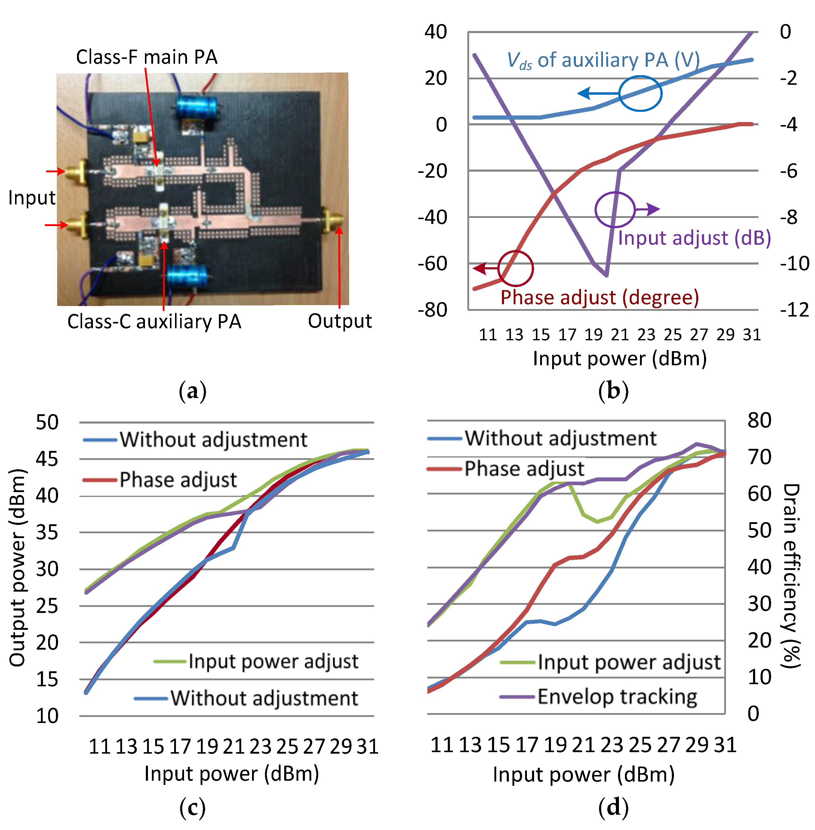
3. Fabrication and Measurement
4. Conclusions
Author Contributions
Funding
Conflicts of Interest
References
- Doherty, W.H. A New High Efficiency Power Amplifier for Modulated Waves. Proc. IRE 1936, 24, 1163–1182. [Google Scholar] [CrossRef]
- Cripps, S. RF power amplifiers for wireless communications. IEEE Microw. Mag. 2000, 1, 64. [Google Scholar] [CrossRef]
- Tasker, P. Practical waveform engineering. IEEE Microw. Mag. 2009, 10, 65–76. [Google Scholar] [CrossRef]
- Musolff, C.; Kamper, M.; Abou-Chahine, Z.; Fischer, G. A Linear and Efficient Doherty PA at 3.5 GHz. IEEE Microw. Mag. 2012, 14, 95–101. [Google Scholar] [CrossRef]
- Giofre, R.; Colantonio, P.; Giannini, F.; Piazzon, L. New Output Combiner for Doherty Amplifiers. IEEE Microw. Wirel. Compon. Lett. 2013, 23, 31–33. [Google Scholar] [CrossRef]
- Modi, S.; Prakash, R.; Yanduru, N.; Balsara, P. A novel efficiency improvement technique for Doherty power amplifiers. In Proceedings of the Texas Symposium on Wireless and Microwave Circuits and Systems, Waco, TX, USA, 3–4 April 2014; pp. 1–4. [Google Scholar]
- Pang, J.; Li, Y.; Chu, C.; Peng, J.; Zhou, X.Y.; Zhu, A. Extend high efficiency range of Doherty power amplifier by modifying characteristic impedance of transmission lines in load modulation network. In Proceedings of the 2020 IEEE/MTT-S International Microwave Symposium (IMS), Los Angeles, CA, USA, 18–27 June 2020; pp. 1–4. [Google Scholar]
- Kim, J.; Fehri, B.; Boumaiza, S.; Wood, J. Power Efficiency and Linearity Enhancement Using Optimized Asymmetrical Doherty Power Amplifiers. IEEE Trans. Microw. Theory Tech. 2010, 59, 425–434. [Google Scholar] [CrossRef]
- Ishikawa, R.; Takayama, Y.; Honjo, K. Fully Integrated Asymmetric Doherty Amplifier Based on Two-Power-Level Impedance Optimization. In Proceedings of the 13th European Microwave Integrated Circuits Conference, Madrid, Spain, 23–25 September 2018; pp. 253–256. [Google Scholar]
- Takagi, Y.; Hasegawa, N.; Ohta, Y.; Ishikawa, R.; Honjo, K. High-Efficiency Asymmetric Doherty Power Amplifier with Spurious Suppression Circuit. In Proceedings of the 50th European Microwave Conference, Utrecht, The Netherlands, 12–14 January 2021; pp. 308–311. [Google Scholar]
- Fang, X.H.; Cheng, K.-K.M. Extension of High-Efficiency Range of Doherty Amplifier by Using Complex Combining Load. IEEE Trans. Microw. Theory Tech. 2014, 62, 2038–2047. [Google Scholar] [CrossRef]
- Xu, Y.; Pang, J.; Wang, X.; Zhu, A. Enhancing Bandwidth and Back-Off Range of Doherty Power Amplifier with Modified Load Modulation Network. IEEE Trans. Microw. Theory Tech. 2021, 69, 2291–2303. [Google Scholar] [CrossRef]
- Bathich, K.; Markos, A.Z.; Boeck, G. A Wideband GaN Doherty Amplifier with 35% Fractional Band-width. In Proceedings of the 40th European Microwave Conference, Paris, France, 28–30 September 2010; pp. 1006–1009. [Google Scholar]
- Gustafsson, D.; Andersson, C.M.; Fager, C. A Modified Doherty Power Amplifier with Extended Bandwidth and Reconfigurable Efficiency. IEEE Trans. Microw. Theory Tech. 2013, 61, 533–542. [Google Scholar] [CrossRef]
- Wu, T.Y.T.; Boumaiza, S. A Modified Doherty Configuration for Broadband Amplification Using Symmetrical Devices. IEEE Trans. Microw. Theory Tech. 2012, 60, 3201–3213. [Google Scholar] [CrossRef]
- Giofre, R.; Piazzon, L.; Colantonio, P.; Giannini, F. An Ultra-Broadband GaN Doherty Amplifier, with 83% of Fractional Bandwidth. IEEE Microw. Wirel. Compon. Lett. 2014, 24, 775–777. [Google Scholar] [CrossRef]
- Fang, X.-H.; Cheng, K.-K.M. Improving Power Utilization Factor of Broadband Doherty Amplifier by Using Bandpass Auxiliary Transformer. IEEE Trans. Microw. Theory Tech. 2015, 63, 2811–2820. [Google Scholar] [CrossRef]
- Zhang, Z.; Cheng, Z.; Li, H.; Ke, H.; Guo, Y.J. A Broadband Doherty Power Amplifier with Hybrid Class-EFJ Mode. IEEE Trans. Circuits Syst. I Regul. Pap. 2020, 67, 4270–4280. [Google Scholar] [CrossRef]
- Kang, H.; Lee, W.; Oh, S.; Oh, H.; Choi, W.; Lee, H.; Hwang, K.C.; Lee, K.-Y.; Yang, Y. Optimized Broadband Load Network for Doherty Power Amplifier Based on Bandwidth Balancing. IEEE Microw. Wirel. Compon. Lett. 2020, 31, 280–283. [Google Scholar] [CrossRef]
- Li, M.; Pang, J.; Li, Y.; Zhu, A. Bandwidth Enhancement of Doherty Power Amplifier Using Modified Load Modulation Network. IEEE Trans. Circuits Syst. I Regul. Pap. 2020, 67, 1824–1834. [Google Scholar] [CrossRef]
- Zhou, X.Y.; Zheng, S.Y.; Chan, W.S.; Chen, S.; Ho, D. Broadband Efficiency-Enhanced Mutually Coupled Harmonic Postmatching Doherty Power Amplifier. IEEE Trans. Circuits Syst. I Regul. Pap. 2017, 64, 1758–1771. [Google Scholar] [CrossRef]
- Naah, G.; Giofre, R. Empowering the Bandwidth of Continuous-Mode Symmetrical Doherty Amplifiers by Leveraging on Fuzzy Logic Techniques. IEEE Trans. Microw. Theory Tech. 2019, 68, 3134–3147. [Google Scholar] [CrossRef] [Green Version]
- Chen, W.; Bassam, S.A.; Li, X.; Liu, Y.; Rawat, K.; Helaoui, M.; Ghannouchi, F.M.; Feng, Z. Design and Linearization of Concurrent Dual-Band Doherty Power Amplifier with Frequency-Dependent Power Ranges. IEEE Trans. Microw. Theory Tech. 2011, 59, 2537–2546. [Google Scholar] [CrossRef]
- Saad, P.; Piazzon, L.; Colantonio, P.; Moon, J.; Giannini, F.; Andersson, K.; Kim, B.; Fager, C. Multi-band/multi-mode and efficient transmitter based on a Doherty Power Amplifier. In Proceedings of the 2012 7th European Microwave Integrated Circuit Conference, Amsterdam, The Netherlands, 29–30 October 2012; pp. 1031–1034. [Google Scholar]
- Mohamed, A.M.M.; Boumaiza, S.; Mansour, R.R. Electronically Tunable Doherty Power Amplifier for Multi-Mode Multi-Band Base Stations. IEEE Trans. Circuits Syst. I Regul. Pap. 2013, 61, 1229–1240. [Google Scholar] [CrossRef]
- Rawat, K.; Ghannouchi, F.M. Design Methodology for Dual-Band Doherty Power Amplifier with Performance Enhancement Using Dual-Band Offset Lines. IEEE Trans. Ind. Electron. 2011, 59, 4831–4842. [Google Scholar] [CrossRef]
- Gustafsson, D.; Cahuana, J.C.; Kuylenstierna, D.; Angelov, I.; Fager, C. A GaN MMIC Modified Doherty PA with Large Bandwidth and Reconfigurable Efficiency. IEEE Trans. Microw. Theory Tech. 2014, 62, 3006–3016. [Google Scholar] [CrossRef]
- Jee, S.; Lee, J.; Son, J.; Kim, S.; Kim, C.H.; Moon, J.; Kim, B. Asymmetric Broadband Doherty Power Amplifier Using GaN MMIC for Femto-Cell Base-Station. IEEE Trans. Microw. Theory Tech. 2015, 63, 2802–2810. [Google Scholar]
- Carneiro, M.L.; Deltimple, N.; Carvalho, P.H.; Belot, D.; Kerhervé, E. Fully integrated CMOS Doherty power amplifier with network matching optimization for die size reduction. In Proceedings of the 2014 44th European Microwave Conference (EuMC), Rome, Italy, 6–9 October 2014; pp. 1269–1272. [Google Scholar]
- Darraji, R.; Kwan, A.K.; Fadhel, M. Ghannouchi, and Mohamed Helaoui. Digitally Equalized Doherty RF Front-End Architecture for Broadband and Multi-standard Wireless Transmitters. IEEE Trans. Microw. Theory Tech. 2015, 63, 1978–1988. [Google Scholar] [CrossRef]
- Park, Y.; Lee, J.; Jee, S.; Kim, S.; Kim, C.H.; Park, B.; Kim, B. GaN HEMT MMIC Doherty Power Amplifier with High Gain and High PAE. IEEE Microw. Wirel. Compon. Lett. 2015, 25, 187–189. [Google Scholar] [CrossRef]
- Fang, X.; Liu, H.; Cheng, K.M.; Boumaiza, S. Two-Way Doherty Power Amplifier Efficiency Enhancement by Incorporating Transistors’ Nonlinear Phase Distortion. IEEE Microw. Wirel. Compon. Lett. 2018, 28, 168–170. [Google Scholar] [CrossRef]
- Kim, I.; Kim, B. A 2.655 GHz 3-stage Doherty power amplifier using envelope tracking technique. In Proceedings of the 2010 IEEE MTT-S International Microwave Symposium, Anaheim, CA, USA, 23–28 May 2010; pp. 1496–1499. [Google Scholar]
- Choi, J.; Kang, D.; Kim, D.; Kim, B. Optimized Envelope Tracking Operation of Doherty Power Amplifier for High Efficiency Over an Extended Dynamic Range. IEEE Trans. Microw. Theory Tech. 2009, 57, 1508–1515. [Google Scholar] [CrossRef]
- Lees, J.; Goss, M.; Benedikt, J.; Tasker, P.J. Single-tone optimization of an adaptive-bias Doherty structure. In Proceedings of the IEEE MTT-S International Microwave Symposium Digest, Philadelphia, PA, USA, 8–13 June 2003; pp. 2213–2216. [Google Scholar]
- Park, Y.; Lee, J.; Jee, S.; Kim, S.; Kim, B. Gate Bias Adaptation of Doherty Power Amplifier for High Efficiency and High Power. IEEE Microw. Wirel. Compon. Lett. 2014, 25, 136–138. [Google Scholar] [CrossRef]
- Fishler, D.; Popovic, Z.; Barton, T. Supply Modulation Behavior of a Doherty Power Amplifier. IEEE J. Microw. 2021, 1, 508–512. [Google Scholar] [CrossRef]


| Freq. (GHz) | 2.1 | Narrow-Band Designed |
|---|---|---|
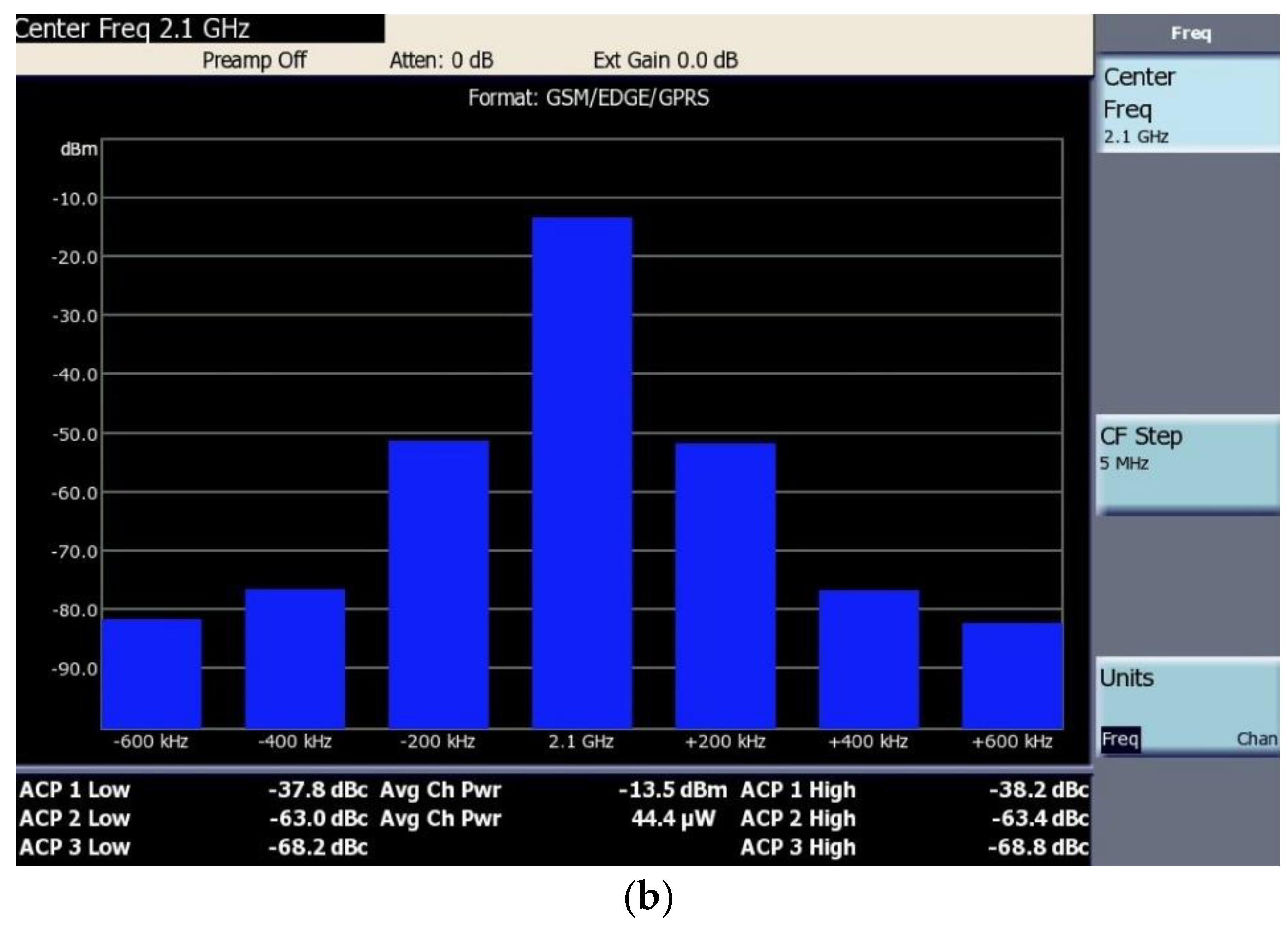
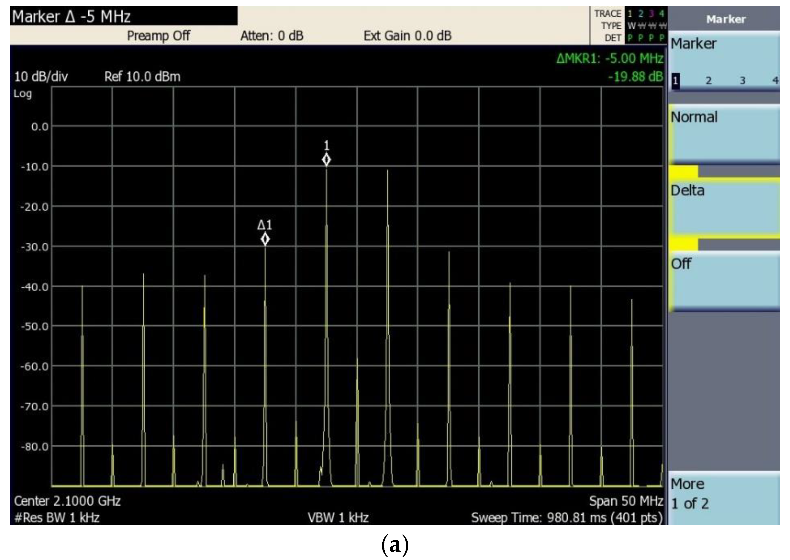
| IM3 (dBc) | 19.88 | Two tones input power of 30 dBm (1-dB back-off from saturation point) |
| ACPR (dBc) | 37.8 | EDGE signal of 200 KHz channel bandwidth and 3.6 dB PAPR, envelop peak at saturation point |
Publisher’s Note: MDPI stays neutral with regard to jurisdictional claims in published maps and institutional affiliations. |
© 2021 by the authors. Licensee MDPI, Basel, Switzerland. This article is an open access article distributed under the terms and conditions of the Creative Commons Attribution (CC BY) license (https://creativecommons.org/licenses/by/4.0/).
Share and Cite
Yang, F.; Li, J.; Yu, H.; Yan, S.; Zhang, A.; Xu, K.; Jin, Z. Asymmetric Doherty Power Amplifier with Input Phase/Power Adjustment and Envelope Tracking. Electronics 2021, 10, 2327. https://doi.org/10.3390/electronics10192327
Yang F, Li J, Yu H, Yan S, Zhang A, Xu K, Jin Z. Asymmetric Doherty Power Amplifier with Input Phase/Power Adjustment and Envelope Tracking. Electronics. 2021; 10(19):2327. https://doi.org/10.3390/electronics10192327
Chicago/Turabian StyleYang, Fei, Jun Li, Hongxi Yu, Sen Yan, Anxue Zhang, Kaida Xu, and Zhonghe Jin. 2021. "Asymmetric Doherty Power Amplifier with Input Phase/Power Adjustment and Envelope Tracking" Electronics 10, no. 19: 2327. https://doi.org/10.3390/electronics10192327
APA StyleYang, F., Li, J., Yu, H., Yan, S., Zhang, A., Xu, K., & Jin, Z. (2021). Asymmetric Doherty Power Amplifier with Input Phase/Power Adjustment and Envelope Tracking. Electronics, 10(19), 2327. https://doi.org/10.3390/electronics10192327