
A High Bandwidth-Power Efficiency, Low THD2,3 Driver Amplifier with Dual-Loop Active Frequency Compensation for High-Speed Applications


Abstract
:1. Introduction
2. Multistage Amplifier Architecture
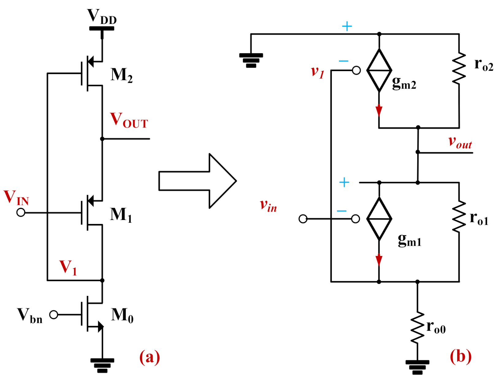
2.1. Zinput Stage and Class-AB Output Stage
2.2. The Flipped Voltage Follower (FVF) Buffer
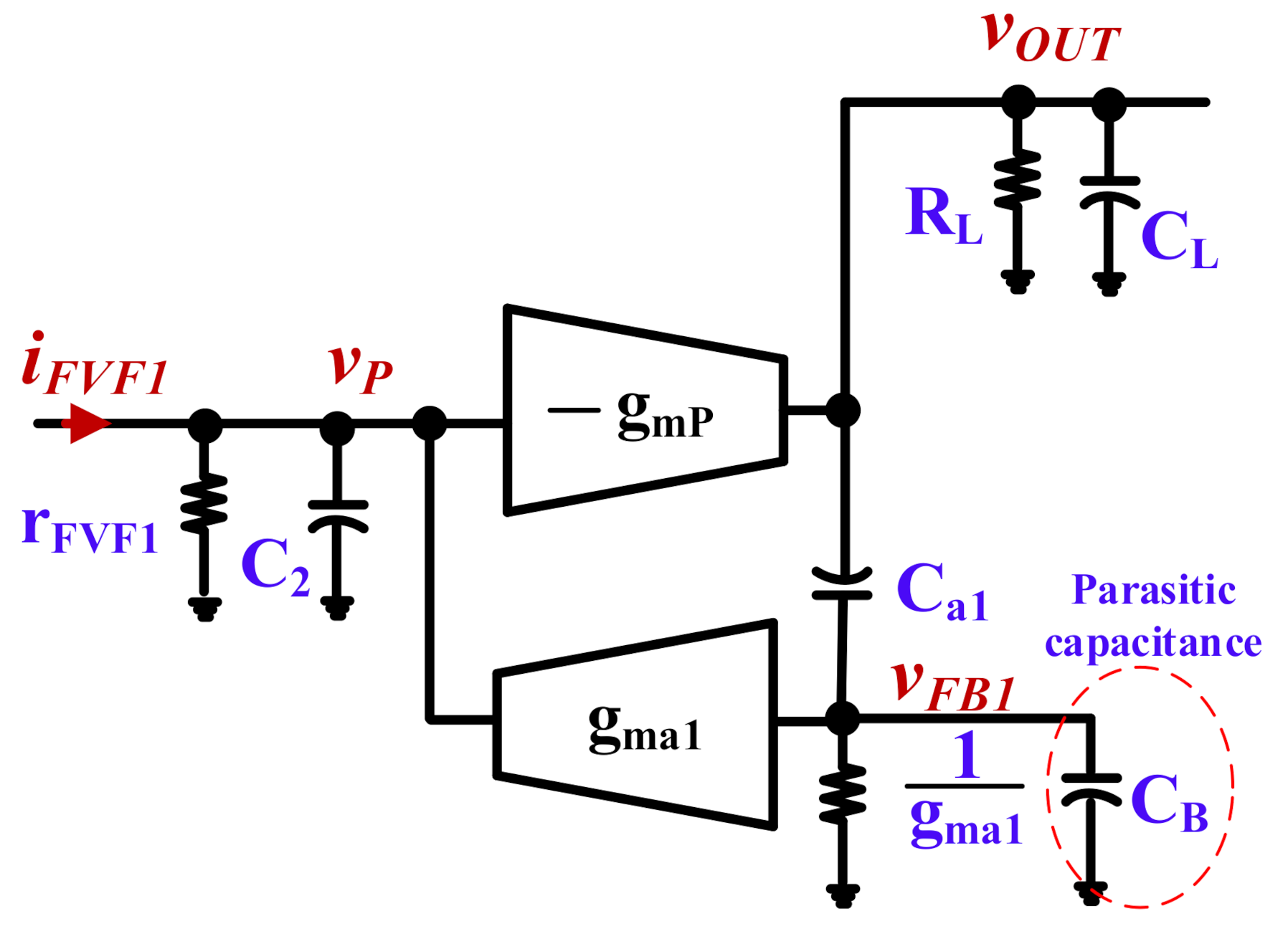
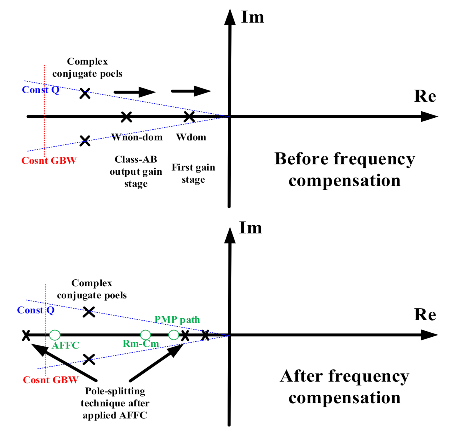
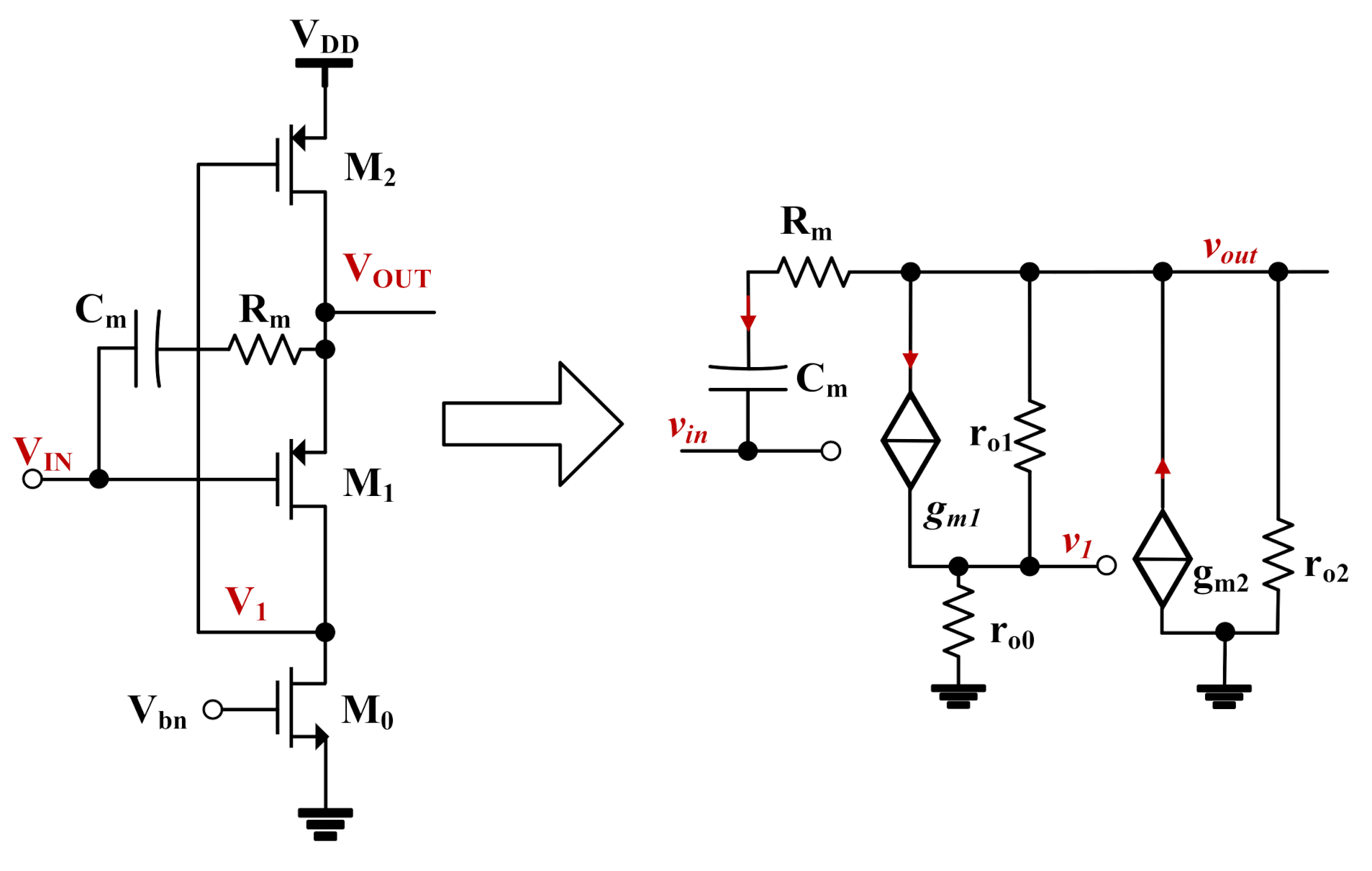
2.3. The Proposed Dual-Loop Active Frequency Compensation
- (1)
- Capacitor is connected in the current buffer configuration in the inner loop, where its advantage is to shift the dominant pole location without any pole-splitting effect to protect the amplifier from PVT variations.
- (2)
- Phase Margin Boosting (PMB) is introduced to achieve nondominant pole compensation by creating 2 low-frequency LHP zeros from the PMB feedback path. A one-pair of Miller capacitor with nulling resistor in parallel with GM,FVF1 is introduced to add 1-pole–zero pair to the inner loop effectively. The extra pole (generated by capacitor with nulling resistor in the second stage) will not influence the amplifier stability because the AFFC network is connected between the FVF buffer stages and the class-AB output stage in cascode frequency compensation to generate pole splitting and to push this extra pole into high-frequency pole (Refer to the pole-zero placement relationship before and after compensation analyzed in the following sections along with systematic complete calculations ). AFFC topology is adopted to reduce the value of and push the dominant pole to higher frequency to obtain better THD+N suppression in higher frequency. The primary function of this RC pair is to create an extra zero along with the AFFC zero effectively: to achieve phase margin boosting (PMB) against the complex poles.
- (3)
- Due to the phase margin loss from the second nondominant pole, it is necessary to introduce an extra LHP zero to achieve low-frequency phase margin protection (PMP). This is done through the PMP path, which effectively adds one more LHP zero () to protect the phase margin.
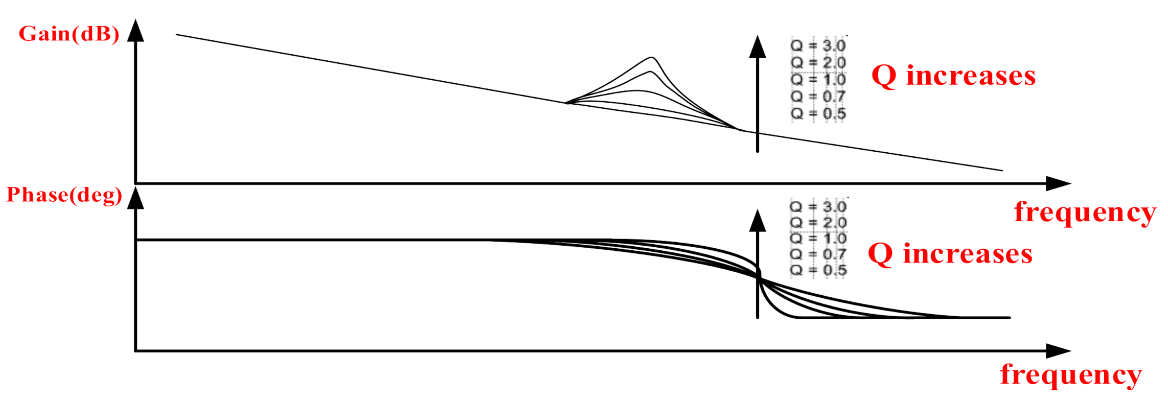
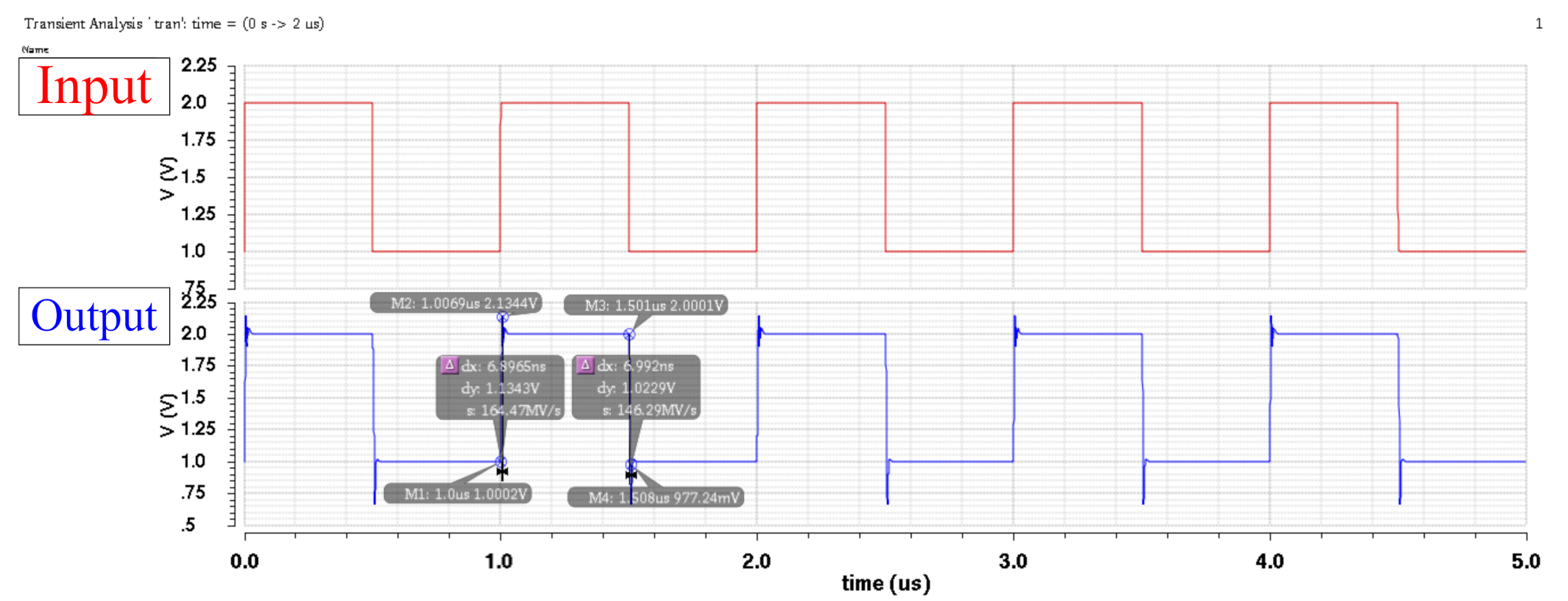
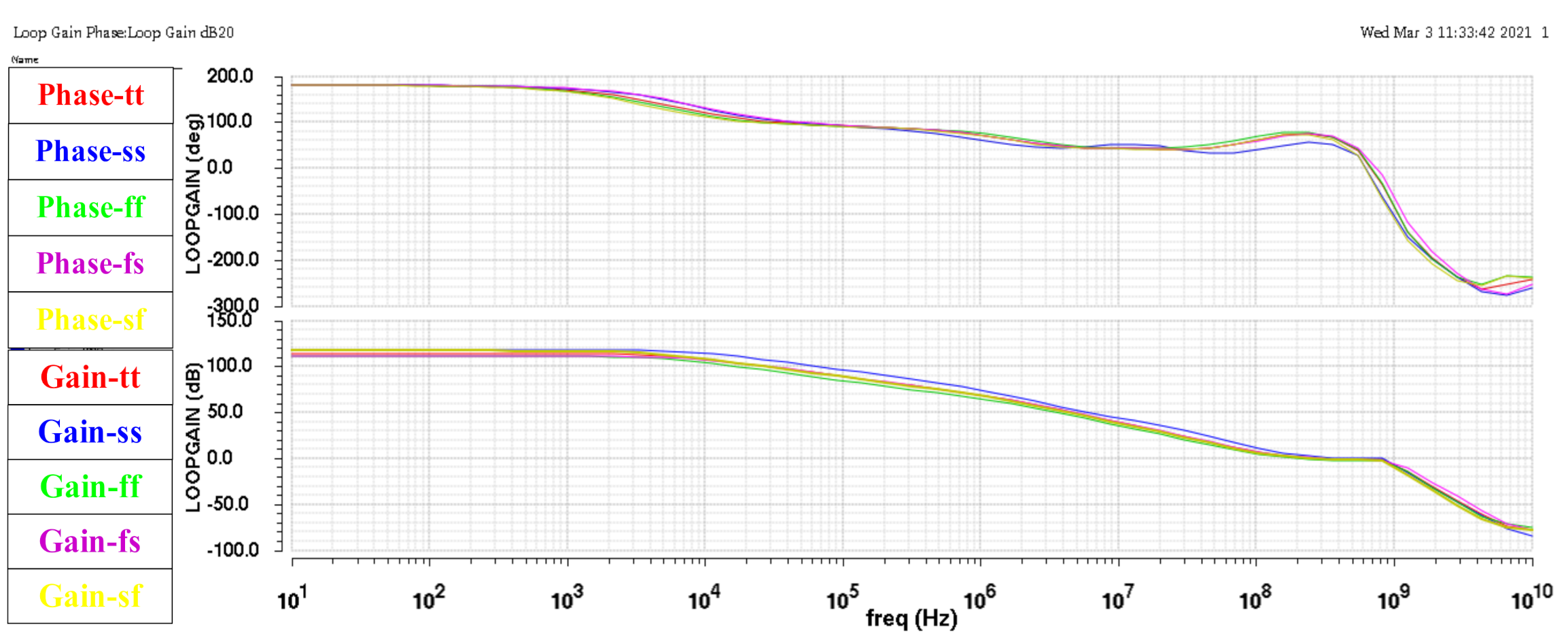
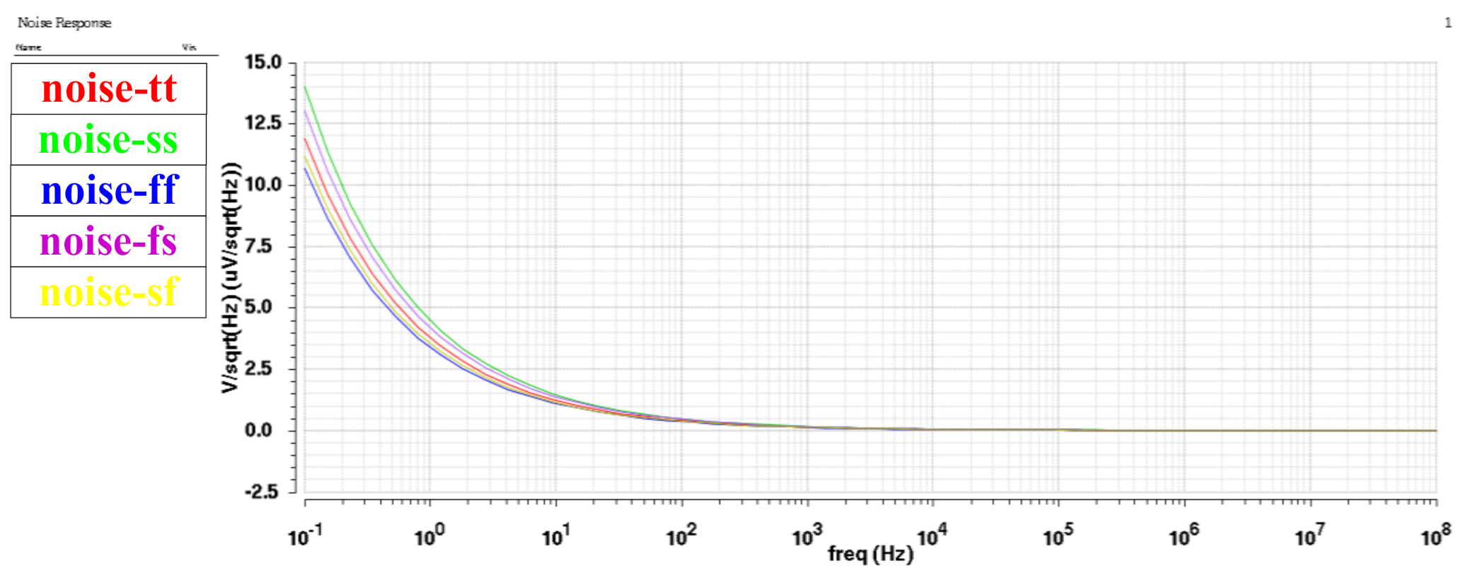
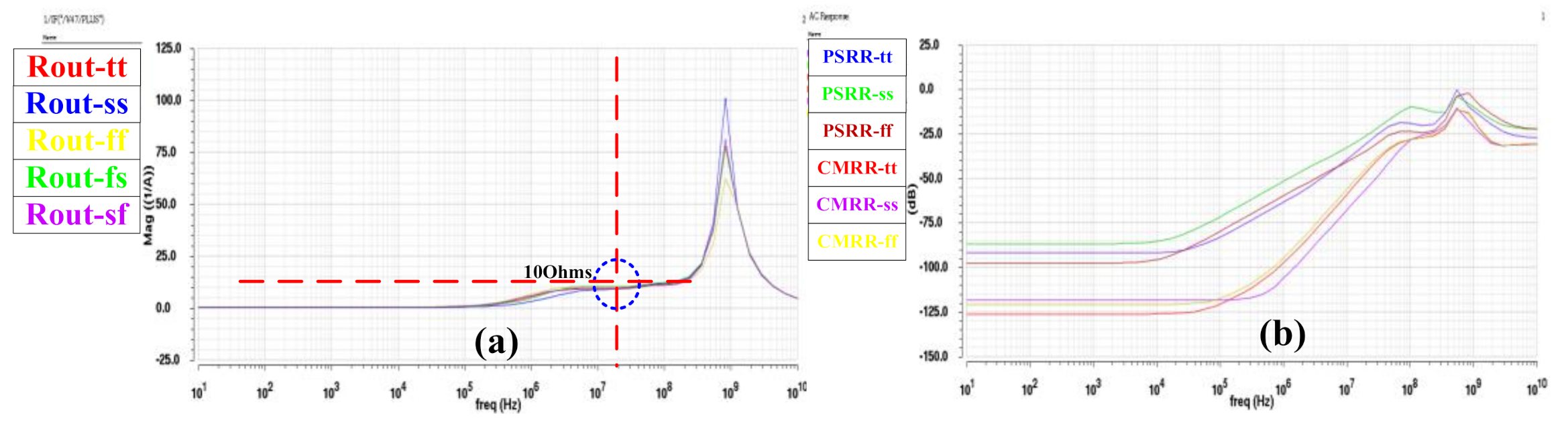
3. Simulation Results and Discussions
4. Conclusions
Author Contributions
Funding
Conflicts of Interest
References
- ADS8881x 18-Bit, 1-MSPS, Serial Interface, microPower, Miniature, True-Differential Input SAR Analog-to-Digital Converter. 2013. Available online: https://www.ti.com/lit/ds/symlink/ads8881.pdf (accessed on 20 September 2020).
- 18-Bit, 1 Msps, Low Power SAR ADC with 102 dB SNR. 2011. Available online: https://www.analog.com/media/en/technical-documentation/data-sheets/237818fa.pdf (accessed on 20 September 2020).
- Very Low Power, Negative Rail Input, Rail-to-Rail Output, Fully-Differential Amplifier. 2008. Available online: https://www.ti.com/lit/ds/symlink/ths4521.pdf (accessed on 20 September 2020).
- Precision, Low Power, Rail-to-Rail Input/Output, Differential Op Amp/SAR ADC Driver. 2012. Available online: https://static6.arrow.com/aropdfconversion/8d56245bbb68812636b982b4323e20a2cb36b113/6362fa.pdf (accessed on 20 September 2020).
- Single Supply, Differential, 18-Bit ADC Driver. 2006. Available online: https://www.analog.com/media/en/technical-documentation/data-sheets/ADA4941-1.pdf (accessed on 20 September 2020).
- Luff, G.F. A 3.3V-Supply 120mW Differential ADC Driver Amplifier in 0.18 μm SiGe BiCMOS. In Proceedings of the IEEE ISSCC, San Francisco, CA, USA, 13–22 February 2011; pp. 250–251. [Google Scholar]
- Kim, J.-S.; Jeong, D.-K.; Kim, G. A multi-level multi-phase charge recycling method for low-power AMLCD column drivers. IEEE J. Solid-State Circuits 2000, 35, 74–84. [Google Scholar]
- Son, Y.-S.; Kim, J.-H.; Cho, H.-H.; Hong, J.-P.; Na, J.-H.; Kim, D.-S.; Han, D.-K.; Hong, J.-C.; Jeon, Y.-J.; Cho, G.-H. A column driver with low-power area-efficient push-pull buffer amplifiers for activematrix LCDs. In Proceedings of the IEEE ISSCC, San Francisco, CA, USA, 11–15 February 2007; pp. 142–143. [Google Scholar]
- Yu, P.-C.; Wu, J.-C. A class-b output buffer for flat-panel-display column driver. IEEE J. Solid-State Circuits 1999, 34, 116–119. [Google Scholar]
- Itakura, T.; Minamizaki, H. A two-gain-stage amplifier without an on-chip miller capacitor in an LCD driver IC. IEICE Trans. Fundam. 2002, E85-A, 1913–1920. [Google Scholar]
- Lu, C.-W.; Lee, C.L. A low power high speed class-AB buffer amplifier for flat panel display application. IEEE Trans. VLSI Syst. 2002, 10, 163–168. [Google Scholar]
- Leung, K.N.; Mok, P.K.T.; Ki, W.H.; Sin, J.K.O. Three-stage large capacitive load amplifier with damping-factor-control frequency compensation. IEEE J. Solid-State Circuits 2000, 35, 221–230. [Google Scholar] [CrossRef]
- Lee, H.; Mok, P.K.T. Active-feedback frequency-compensation technique for low-power multistage amplifiers. IEEE J. Solid-State Circuits 2003, 38, 511–520. [Google Scholar] [CrossRef]
- Leung, K.N.; Mok, P.K.T. A capacitor-free CMOS low-dropout regulator with damping-factor-control frequency compensation. IEEE J. Solid-State Circuits 2003, 38, 1691–1702. [Google Scholar] [CrossRef]
- Ho, E.N.Y.; Mok, P.K.T. A capacitor-less CMOS active feedback low-dropout regulator with slew-rate enhancement for portable on-chip application. IEEE Trans. Circuits Syst. II Exp. Briefs 2010, 57, 80–84. [Google Scholar] [CrossRef]


| Definition | Expression |
|---|---|
| DC gain | |
| Dominant pole | |
| Nondominant pole | |
| High-frequency pole | |
| Low-frequency LHP zero | |
| High-frequency LHP zero 1 | |
| High-frequency LHP zero 2 |
| Parameter | 1 This Work | ** [3] | ** [4] | ** [5] | ** [6] |
|---|---|---|---|---|---|
| Technology | DBH-0.18 µm | Bipolar/BICMOS | Bipolar/BICMOS | Bipolar/BICMOS | 0.18 µm BICMOS |
| Supply | 5 | 5 | 5 | 5 | 3.3 |
| Power (mW) | 12.5 mW | 5.7 mW | 5 mW | 11 mW | 120.12 mW |
| A0 (dB) | 115 | 70 | 45 | 33 | 97 |
| GBW (MHz) | 250 | 50 | 34 | 30 | 2200 |
| SR (V/µs) | 265 | 490 | 45 | 22 | |
| Input referred noise | 5 nV/ @1 MHz | 5.7 nV/ @1 MHz | 6.4 nV/ @1 MHz | 5.1 nV/ @1 MHz | 1.67 nV/ @1 MHz |
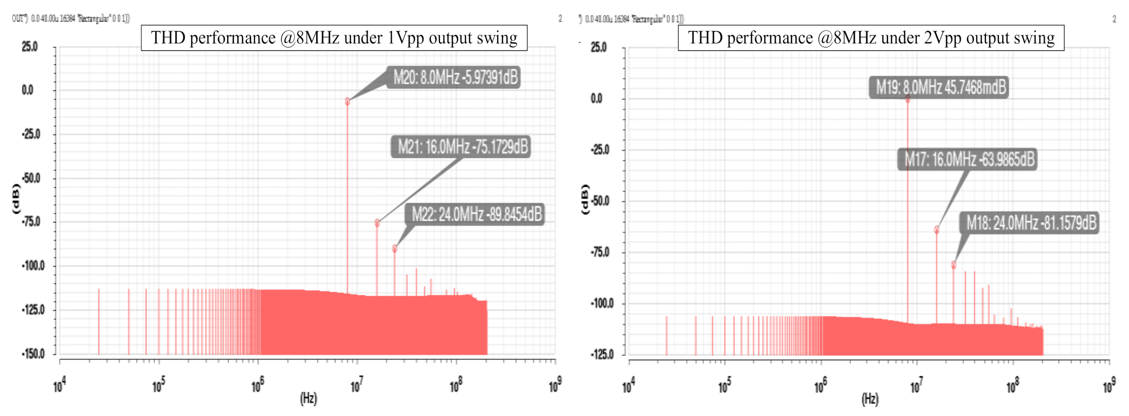
| HD2,3 @ (1 MHz output swing (1 V, 2 V) | 16.5-bit 16-bit (−109/128) (−98/106) | HD2,3 at 10 kHz (dB) −133/140 | HD2,3 at 10 kHz −106/−103 | HD2,3 at 10 kHz (dB) −125/−126 | HD2,3 at 10 kHz (dB) −74/−101 |
| HD2,3 @ (8 MHz) output swing (1 V, 2 V) | 14-bit 13.5-bit (−75/−89) (−63/−81) | ||||
| Input offset (µV) | 85 | 2000 | 200 | 360 | ----------- |
Publisher’s Note: MDPI stays neutral with regard to jurisdictional claims in published maps and institutional affiliations. |
© 2021 by the authors. Licensee MDPI, Basel, Switzerland. This article is an open access article distributed under the terms and conditions of the Creative Commons Attribution (CC BY) license (https://creativecommons.org/licenses/by/4.0/).
Share and Cite
Fu, X.; El-Sankary, K.; Yin, Y. A High Bandwidth-Power Efficiency, Low THD2,3 Driver Amplifier with Dual-Loop Active Frequency Compensation for High-Speed Applications. Electronics 2021, 10, 2311. https://doi.org/10.3390/electronics10182311
Fu X, El-Sankary K, Yin Y. A High Bandwidth-Power Efficiency, Low THD2,3 Driver Amplifier with Dual-Loop Active Frequency Compensation for High-Speed Applications. Electronics. 2021; 10(18):2311. https://doi.org/10.3390/electronics10182311
Chicago/Turabian StyleFu, Ximing, Kamal El-Sankary, and Yadong Yin. 2021. "A High Bandwidth-Power Efficiency, Low THD2,3 Driver Amplifier with Dual-Loop Active Frequency Compensation for High-Speed Applications" Electronics 10, no. 18: 2311. https://doi.org/10.3390/electronics10182311
APA StyleFu, X., El-Sankary, K., & Yin, Y. (2021). A High Bandwidth-Power Efficiency, Low THD2,3 Driver Amplifier with Dual-Loop Active Frequency Compensation for High-Speed Applications. Electronics, 10(18), 2311. https://doi.org/10.3390/electronics10182311