1. Introduction
Nonvolatile flash memories are often applied for storage systems that require high data reliability, e.g., industrial robots, scientific and medical instruments. Flash memories are resistant to mechanical shock and provide fast read access times. The information is stored in floating gate transistors that hold the charge in the absence of power [
1,
2,
3]. The cells can be programmed and erased. To distinguish the charge levels and read the stored information, several reference voltages are applied to the control gate. However, this reading operation can cause additional disturbances which lead to errors in stored information [
4].
Due to the error characteristics of the flash memory, it is necessary to use error correction coding (ECC) to guarantee reliability and data integrity [
1,
4,
5,
6]. Traditionally, Bose–Chaudhuri–Hocquenghem (BCH) codes with so-called hard-input decoding were used for error correction [
7,
8]. The term hard-input refers to a reading procedure where only a single bit of information is read from each cell. However, the performance of error correction can be improved with soft-input decoding. Soft-input decoding algorithms utilize reliability information about the state of the cells, where the channel output is quantized using a small number of bits [
9,
10]. Low-density parity-check (LDPC) codes [
11,
12,
13,
14,
15], generalized concatenated codes (GCC) [
16,
17,
18], and polar codes [
19,
20] were proposed for flash memories with soft-input decoding.
The error probability of the flash cells depends on the flash memory technology (single-level cell (SLC), multilevel cell (MLC), triple-level cell (TLC), or quad-level cell (QLC)), the storage density, and the number of programming and erasing cycles. A lot of research exists on the error characteristics considers the flash memory endurance [
1,
21,
22,
23], i.e., the number of program/erase (P/E) cycles. Over time, charge losses occur, which cause a change of the threshold voltage distribution [
24]. In many applications, data retention time is more important than flash endurance. Likewise, read disturb, inter-cell interference, and temperature related charge losses occur [
25,
26,
27,
28]. Such charge losses result in shifts of the threshold voltages. These voltage shifts increase the bit error probability if the reference voltages are not adapted to the actual life cycle conditions.
Compared with hard-input read operation, the threshold voltage sensing operation to obtain the soft information causes a larger latency and a higher energy consumption [
29]. Hence, the soft-input decoding should only be used for blocks where the hard-input decoding fails. Algorithms that adapt the read references can reduce the latency and energy consumption by avoiding soft-reads. Moreover, many soft-input decoding approaches assume reading procedures that maximize the mutual information (MI) between the input and output of flash memory. This requires an accurate adaptation of the read voltages and additional estimation of log-likelihood ratios (LLR) for the quantization intervals [
15,
22].
Several publications proposed threshold adaptation concepts [
25,
30,
31,
32,
33,
34,
35]. These approaches adjust the read references to minimize bit error rates. For instance, the flash controller may apply a read-retry mechanism to adapt the reference voltages. Firstly, the controller reads the data with the default read reference. If the ECC decoder corrects the errors, there is no need to adjust the default value. In the case of decoding failures, the flash controller can perform repeated reads with certain threshold voltages until all errors are corrected by the decoder. However, such read-retry mechanisms can be very time-consuming.
To obtain statistical information about the cell state, a sensing directed estimation method was proposed in [
31]. This method approximates the threshold voltage distribution as a Gaussian mixture. It estimates the mean and standard deviation values based on measured distributions. This scheme does not utilize any known pilot bits but employs extra memory sensing operations similar to the read-retry mechanisms. Such voltage sensing operations incur a larger energy consumption and a latency penalty. Similarly, a parameter estimation approach and a threshold adaptation policy is derived in [
33]. This adaptation method is also based on the assumption of Gaussian voltage distributions. However, the cell threshold voltage distributions of MLC and TLC are actually highly asymmetric with exponential tails [
23,
36,
37] and cannot be estimated with Gaussian distribution. In [
25,
30], coding methods based on Berger codes are suggested that exploit the asymmetric error probabilities of the channel. Berger codes are used for error detection. They can detect any number of one-to-zero errors, as long as no zero-to-one errors occurred in the same codeword. Likewise, Berger codes can detect any number of zero-to-one errors, as long as no one-to-zero bit-flip errors occur in the same code word. However, Berger codes cannot correct any errors.
In this work, we propose two methods for reference calibration that aim on minimizing the BER. Similar to the methods proposed in [
32,
34], we exploit the error correction code to obtain information about the cell state. Based on the number of observed errors in the read codeword, we predict the shift of the reference voltages. It is demonstrated that the observed number of errors is a good feature for the voltage shifts and is utilized for the initial calibration of the read thresholds. However, the total number of errors is only a good measure if there is a relatively large difference between the threshold for the first readout and the optimal read threshold. On the other hand, the total number of errors is not suited to estimate small changes of the read voltages, which occur for different pages from the same block. To cope with this issue, we propose a second approach which is a gradual channel estimation method. Like the approach based on Berger codes, we exploit the asymmetric error probabilities by counting the one-to-zero and zero-to-one errors independently. Based on the asymmetry, we apply a tracking method to adjust the read references from page to page.
We use information-theoretic measures to investigate the relation between the optimal read references and the statistical information obtained by counting errors. Both methods are investigated utilizing the mutual information between the optimal read voltage and the measured error values. Mutual information is also used to determine the parameters for the adaption algorithms. Numerical results based on flash measurements demonstrate that both methods can significantly reduce the BER of NAND flash memories and achieve nearly optimal performance.
This publication is organized as follows. In
Section 2, we review some basic properties of flash memories and introduce a model for the threshold distributions. In
Section 3, we present measurement results that motivate the proposed adaption methods and describe the principal approach. Moreover, we introduce the information-theoretical measures that are used to analyze and optimize the threshold calibration. The calibration of the read reference voltages is detailed in
Section 4, and the gradual estimation method in
Section 5. Finally, we conclude our work in
Section 6.
2. Models for Voltage Distributions and Measurement Data
In this section, we discuss some basic properties of flash memories and introduce the notation. Furthermore, we consider a model to estimate the threshold voltage distributions. This curve fitting approach is used to determine the optimal read voltages.
Flash memory consists of transistors which have an insulated floating gate below the control gate. The information is stored as electric charges in the floating gate. The charge levels affect the threshold voltage of the transistor. The cell can be charged by applying a high program voltage to the control gate and erased by applying a high erase voltage to the substrate. The information can be read out by applying a reference threshold to differentiate erased and charged cells. The cells are organized in arrays of blocks and pages, where the control gates of the cells inside a page are connected using the so-called word line. Multiple pages constitute a block by connecting the drain of one cell to the source of the next cell. These connections form the bit lines.
2.1. Threshold Voltage Distributions
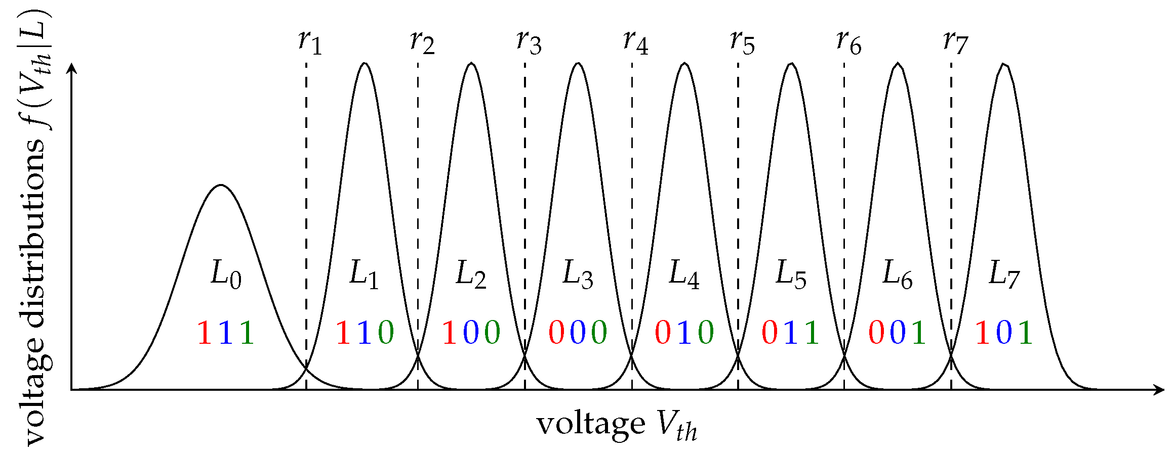
NAND flash technologies are differentiated by the number of bits stored per cell. While SLC flash stores only one bit per cell, TLC flash stores three bits per cell. Hence, a TLC flash requires eight different charge levels (
) and seven reference voltages (
) to read all three bits. The three bits of each cell are typically mapped to three different pages called MSB-, CSB-, and LSB-page, where MSB, CSB, and LSB stand for most significant bit, center significant bit, and least significant bit, respectively.
Figure 1 illustrates the conditional distributions
of the threshold voltages
of the flash cells given the charge levels. The figure also provides a possible bit-labeling for the charge levels, where the colors indicate the corresponding page, i.e., MSB in red, CSB in blue, and LSB in green. Most flash memories support page-wise read operations. For instance, to read the MSB-page with the bit-labeling in
Figure 1, we need to read at the reference voltages
and
.
The distributions are not static but change over the lifetime of the flash. Two of the most important factors for these changes are the number of program/erase (P/E) cycles and the data retention time. The P/E cycles lead to a wear-out of the floating gate, while the data retention time leads to a charge loss. The distributions also depend on effects such as the program and read temperature and the charges of adjacent cells. Moreover, they can vary over pages and blocks.
The threshold distributions can be measured by successively applying all possible threshold voltages and counting the number of cells that are activated for the given voltage and charge level. For those measurements the data retention time is simulated by baking the chip for a specific time [
38,
39].
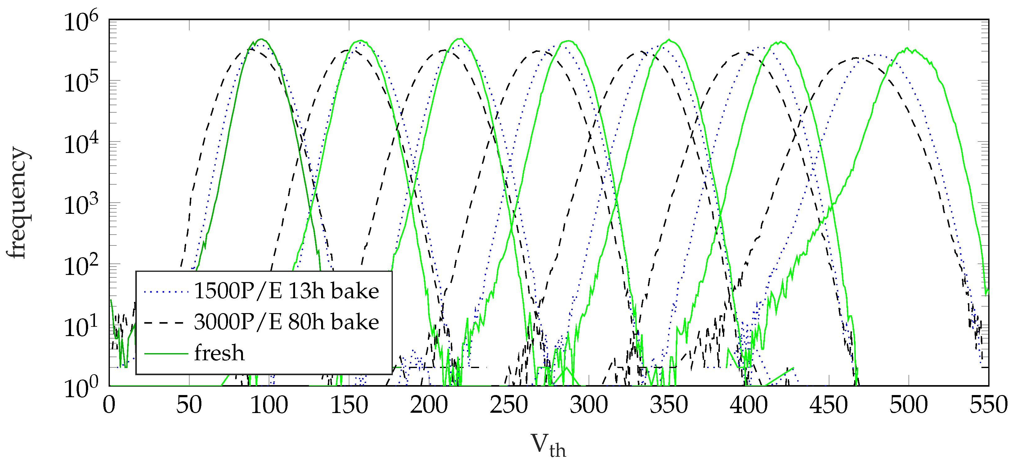
Figure 2 shows measured histograms for three different life-cycle states. The measurements were performed using fresh cells, cells with 1500 P/E-cycles and 13 h of baking, which simulates about two months of data retention, and cells with 3000 P/E-cycles and 80 h of baking, which corresponds to the end of life (EOL) defined by the manufacturer. Note that only the charged states
to
are shown. The voltages are represented by the index numbers of the possible voltage steps.
This figure shows the charge loss due to data retention time as well as the widening of the distributions due to wear-out. Due to the logarithmic scale of the y-axis, it is apparent that the distributions are not symmetric and the voltages are not normally distributed. While the threshold voltage distributions are often modeled as Gaussian distributions, the measured distributions show an exponential tail toward the lower voltages. To cope with this exponential tail, the exponentially-modified Gaussian distribution was proposed [
23] which is the sum of two independent normal and exponential random variables. In [
40], a Normal–Laplace mixture model was proposed. Similarly, the model in [
41] copes with program errors in MLC-Flash memory. In our measurements, all three bit-pages are programmed simultaneously; hence, no write errors happen. Moreover, neither the exponentially-modified Gaussian distribution nor the Normal–Laplace mixture model is able to fit our measurements because these models do not allow for an inflection point, as observed in the measurement data.
2.2. Parameter Estimation
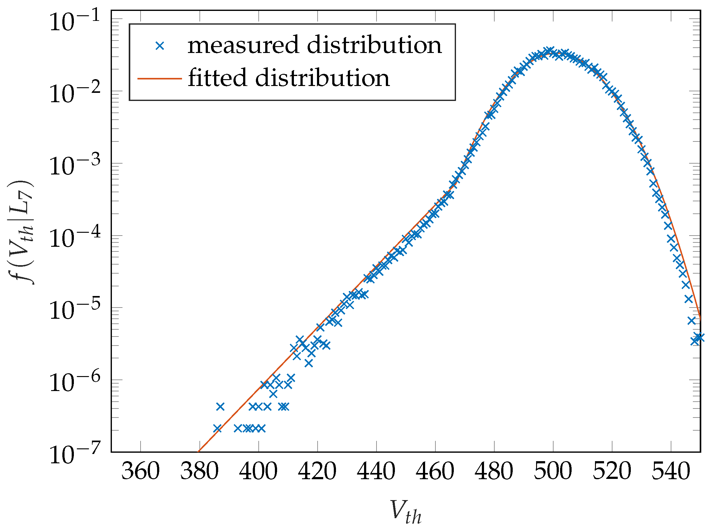
To approximate the measured distributions, we use a parameter estimation approach presented in [
37]. The distributions
are modeled by a piecewise-defined function
with
With the cumulative distribution function
of the standard normal distribution
ensures the normalization
The proposed model requires four parameters, i.e.,
and
. We model the exponential tail to the left by an exponential distribution and the rest by a normal distribution. This leads to a precise estimation of the measured distributions, which is shown by the fitted curve in
Figure 3. This figure shows measurements of the voltage distribution
of a fresh memory together with a fitted distribution.
The magnitude of the skewness of the measured distributions is very small. Consequently, the parameters and can be computed from the sample mean and the sample variance, as the effects of the exponential tail on the mean and variance can be neglected. For the exponential distribution, a least squares regression line is fitted to the logarithm of the measured distribution. The distributions of the lower states also have an exponential tail towards the higher voltages, which is not modeled as it is negligible compared with the tail to lower voltages.
We use the curve fitting to determine the optimal threshold voltage
for each read reference such that the bit error probability is minimized, i.e., the optimal threshold voltage is defined as
2.3. Measurement Data
Note that the measured distributions are also conditioned on the life-cycle state, i.e., the number of P/E-cycles and data retention time, amongst many others. Since the distributions may vary over pages and blocks, the page and block numbers are also conditions of the distributions. For simplicity, we omit those conditions in the notation. To obtain the unconditioned distributions, we would need measurements of all possible life-cycle states together with their a priori probabilities, which depend on the usage.
The measurements used in this work are 185 data sets each consisting of one block with 256 pages. The measurements are from eight different samples of the same flash memory model. The blocks were chosen uniformly over all available blocks on the chip. For the life-cycle states, the P/E cycles were measured up to 3000 in steps of 200 cycles. The data retention time simulated by baking was measured at and 83 h of baking, where 83 h simulates one year. The value 3000 P/E with 83 h baking corresponds to the EOL state defined by the manufacturer. Additionally, measurements of read disturb as well as cross temperature effects were taken into account. For the read disturb, many read cycles were performed before the measurements. For the cross temperature effects, the pages were either programmed at and read at a or the other way around, while the data sets without cross temperature effects were measured at . Most data sets combine several effects.
3. Problem Statement and Principal Approach
This section presents measurement results that motivate the suggested adaptation methods. We describe the principal approach. Moreover, we introduce the information-theoretical measures that are used to analyze and optimize the threshold calibration.
The voltage distributions of a flash memory change over the lifetime. Hence, a constant read reference voltage cannot minimize the bit error rate and the number of errors can surpass the error correction capability of the ECC decoder. To prevent this, the read reference voltage has to be adapted to the current life-cycle state of the flash to minimize the bit error rate. In this section, we discuss and analyze the statistical features that are used for the voltage adaptation.
Similarly to the methods proposed in [
32,
34], we exploit the error correction code to obtain information about the cell state. Based on the error correction code, we can determine the number of errors and the asymmetry of the error distribution, i.e., the probabilities of 1-to-0 errors and 0-to-1 errors are not equal [
23,
25,
30,
42]. In a nutshell, the number of errors provides information about the distance to the optimal threshold and the asymmetry provides information about the direction, i.e, whether to increase or decrease the threshold voltage. We use information-theoretic measures to investigate the relation between the optimal read references and the statistical information obtained by counting errors.
3.1. Asymmetric Error Probabilities
In [
23,
25,
30,
42], asymmetric error probabilities of the flash channel are reported, i.e., the probabilities of 1-to-0 errors and 0-to-1 errors are not equal. In our measurements, we found basically two causes for this asymmetry. Firstly, for some charge levels, the asymmetric shape of the threshold voltage distributions causes a certain asymmetry for the bit errors. Secondly, an offset of the reference voltage leads to asymmetric probabilities of 1-to-0 errors and 0-to-1 errors. Later on, we will exploit the asymmetric error probabilities due to the offsets for the adaptation of the read references.
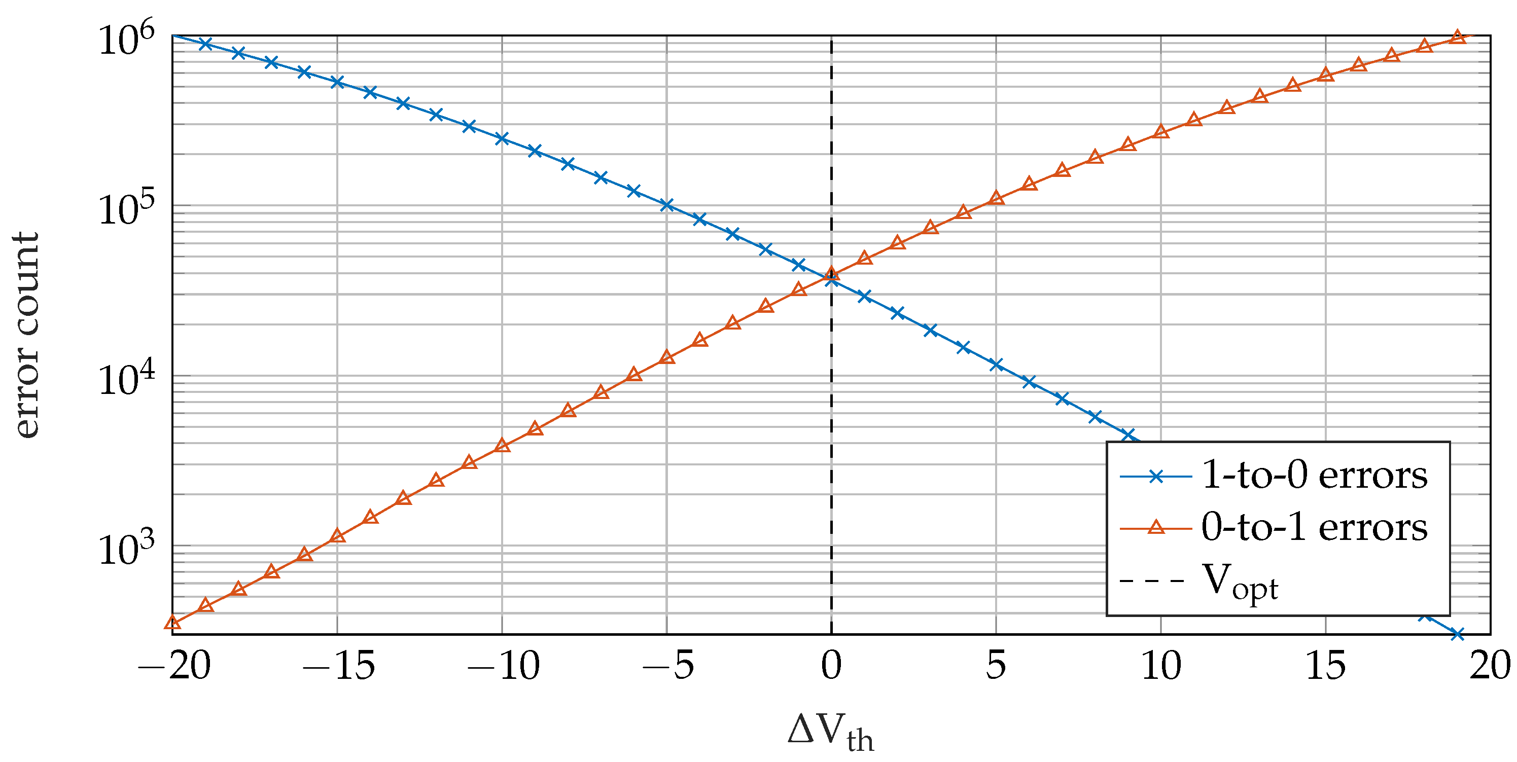
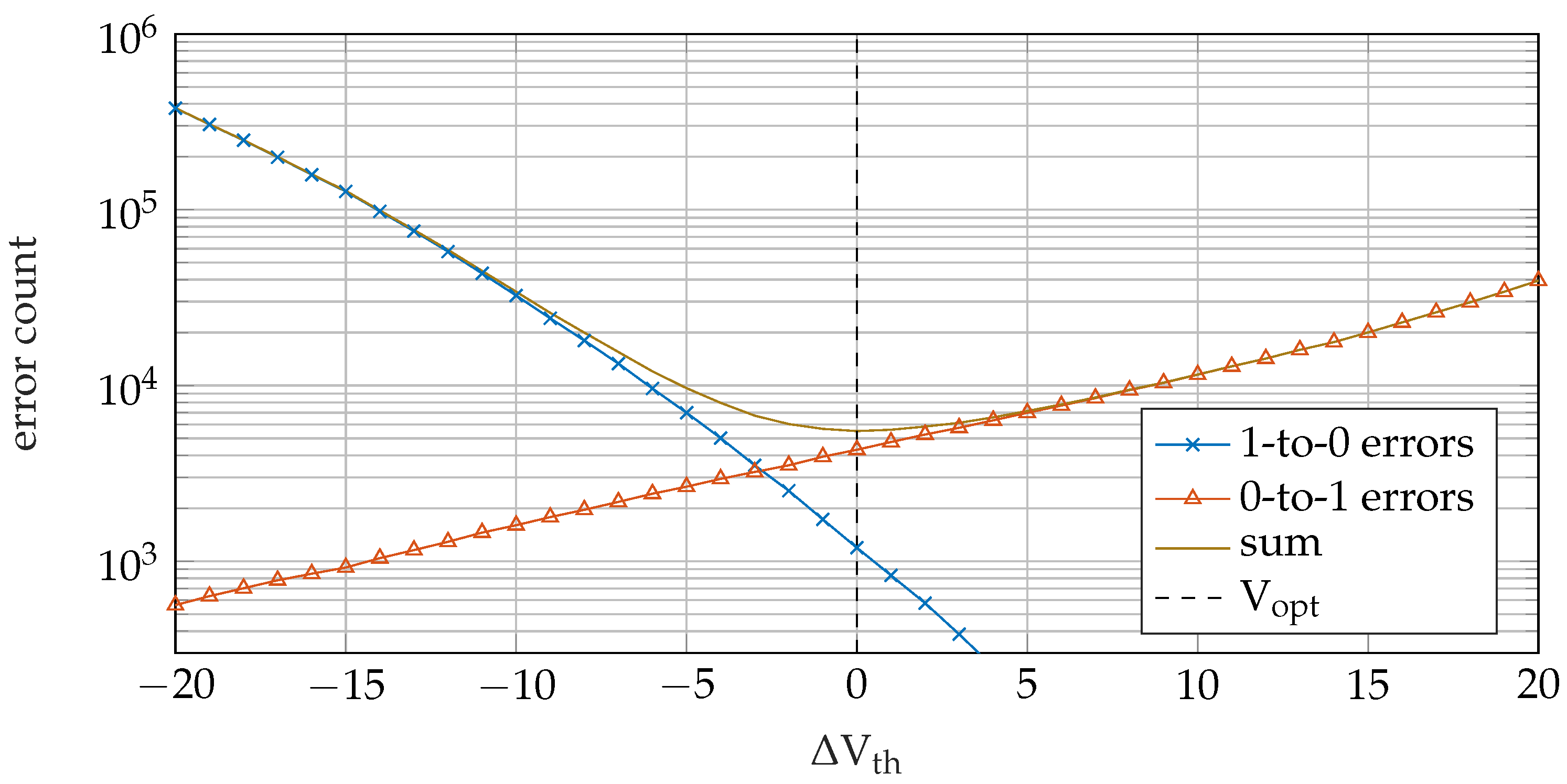
The asymmetric error probabilities are indicated in
Figure 4 which shows the number of errors for 1-to-0 errors and 0-to-1 errors. This figure considers reference
at an EOL scenario. The error probabilities are balanced for the optimal threshold voltage which is indicated by the value
, whereas the asymmetric error counts for other voltages can be exploited for the threshold adaptation.
As shown in
Figure 2, the higher distributions are highly asymmetric for early-life cases.
Figure 5 shows the error count for 1-to-0 errors, 0-to-1 errors, and the overall error count for reference
for a fresh memory block. The error probabilities are asymmetric at the optimal threshold voltage indicated by the value
, which needs to be considered for voltage adaptation.
3.2. Number of Errors
Typically, different error correction codes are applied for the user-data and for meta data. Along with the user-data, a flash controller stores meta information about the life-cycle state, e.g., the number of P/E cycles. Typically, the meta data is protected by a significantly better error correction code than the user-data. Hence, it is possible to correct the errors in the codeword of the meta ECC even at a relatively large offset in the reference voltage. On the other hand, the number of bits for the meta data is small. Consequently, the number of errors in the meta ECC is not always a statistically relevant sample size.
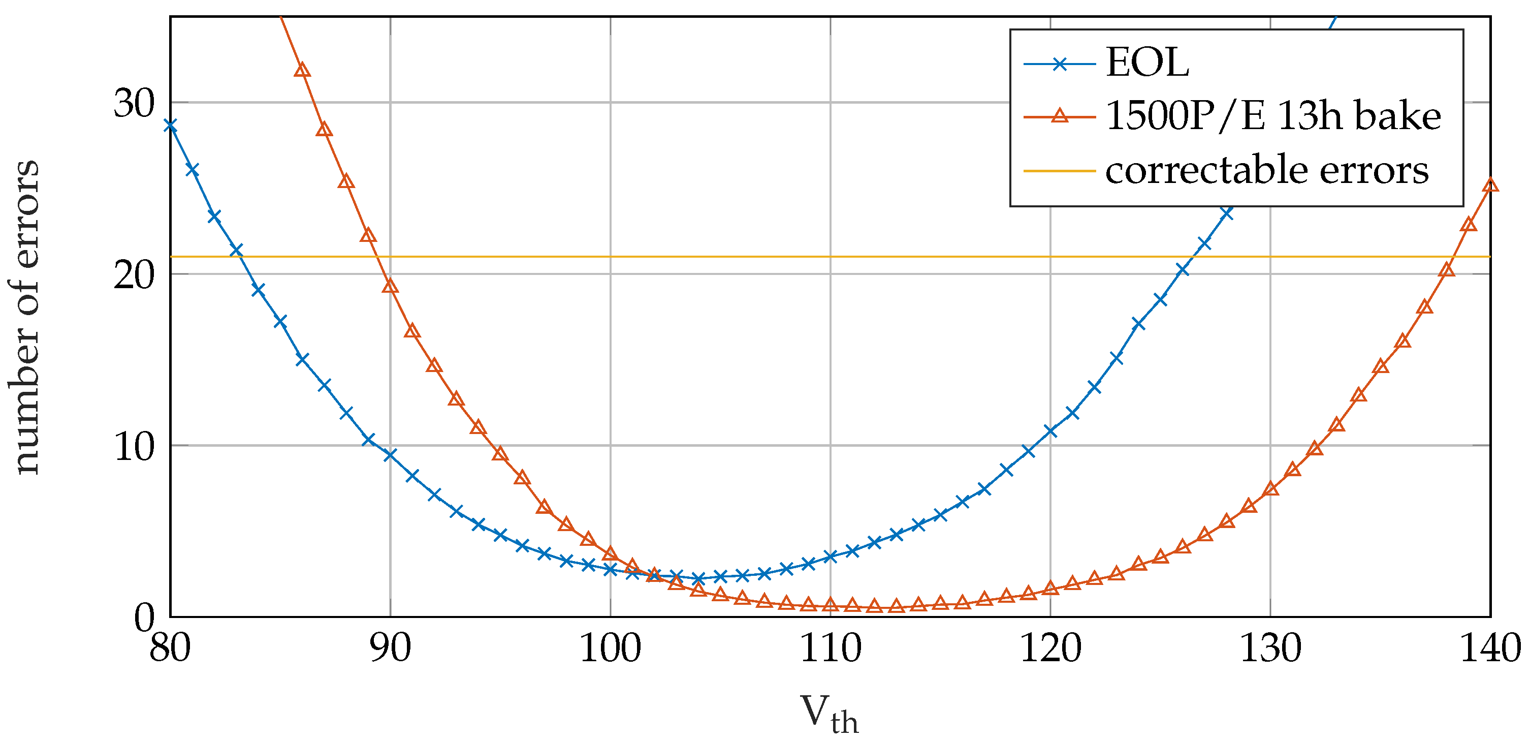
Figure 6 illustrates the number of errors in the meta-data versus the read threshold at different life-cycle states. We consider a code with length
with a correction capability of up to
errors. The horizontal line in
Figure 6 indicates the maximum number of correctable errors. The number of errors for a given voltage provides information about the flash aging. For instance, consider the value
. For the EOL condition, we observed 11 errors on average, whereas the expected number of errors for 1500 P/E cycles is only about two. Hence, the observed number of errors enables a prediction of the offset to the optimal read voltage. However, the provided information depends on
. In
Figure 6, the slope of the error curves is very low near the optimum. When threshold voltages close to the optimal voltage
are applied, only little information is gained by the number of errors. On the other hand, if the offset between
and
is too large then the read data is likely to be undecodable. We use the mutual information between the optimal reference voltage
and the observed number of errors to measure the information that is gained by counting errors.
3.3. Mutual Information
Next, we investigate the information that is obtained by counting the number of errors in the read codewords. Later, we predict the shift of the reference voltages based on the number of observed errors in the read codeword. In addition to the total number of errors, we exploit the asymmetry between 0-errors and 1-errors.
We use information theoretic measures to investigate the relation between the optimal read references and the statistical information obtained by counting errors. In particular, we consider the mutual information. The mutual information
of two random variables is a measure for the information in bits gained about one variable when knowing the other variable. Let
X and
Y be two random variables with
and
with probability distributions
and
and joint probability distribution
. The mutual information between
X and
Y is defined as [
43]
The mutual information is non-negative and upper bounded by the minimum of the entropies of the two variables [
43]. For practical applications, it can have advantages using other measures, e.g., the residual error rate of a given decoder. But those measures are very specific to a given implementation.
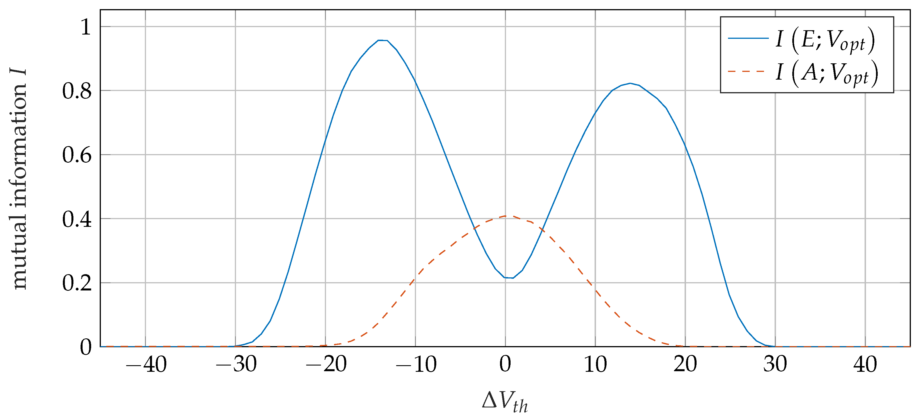
Figure 7 shows the mutual information
between the optimal reference voltage
and the observed number of errors
E. The mutual information is determined over different life-cycle states. As a second observation, we consider a binary random variable
A, which indicates the direction of the asymmetry between 0-errors and 1-errors.
indicates more 1-errors, and
indicates more 0-errors. The mutual information
is also depicted in
Figure 7. Note that this figure shows the curves for reference
.
When using the number of errors in the meta-data, we get the maximum information about the optimum reference when reading at about , i.e., 14 voltage steps lower than the mean optimum reference. Near the optimum, the mutual information is fairly low, and this is due to the fact that the entropy of the number of errors is low in that region. Reading far from the optimum (), we obtain no information about because the read data is not correctable. In the case of a decoding failure, the exact number of errors remains unknown. Near the optimum , we can see that the binary variable A that indicates the asymmetry provides more information about than the number of errors E.
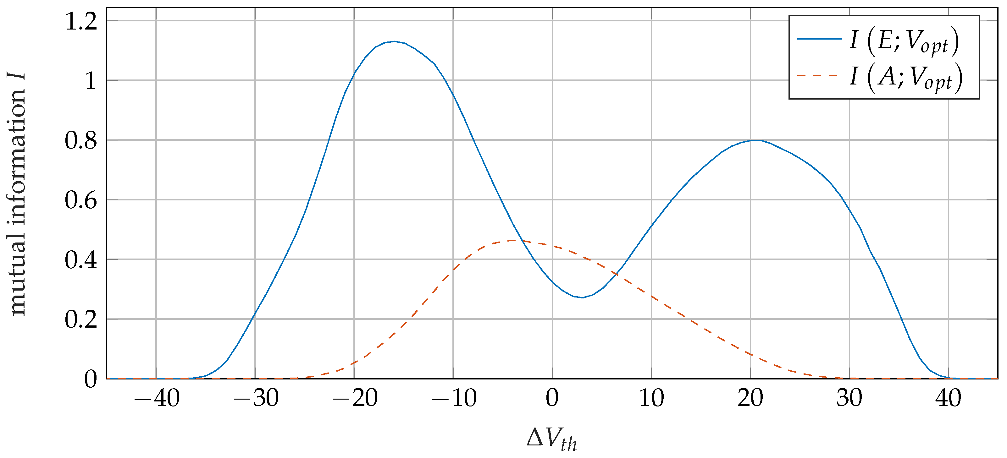
The asymmetry for higher charge values shown in
Figure 5 also leads to an asymmetry in the mutual information. This can be seen in
Figure 8, where the mutual information versus the read voltage is plotted for reference
. As we can see, the maximum of the mutual information between the asymmetry
A and the optimum threshold voltage is not at
. Similarly, the local minimum for
does not occur at
.
3.4. Principal Approach
In the following, we consider two adaptation methods depending on the a priori knowledge about the life-cycle state of the block. Firstly, a calibration approach aims on finding a good reference threshold with a small number of read attempts when we have no knowledge about the life-cycle state. Secondly, a tracking approach, based on a gradual channel estimation method, adjusts the read threshold while iterating over successive pages, i.e., we calibrate the first page of a block and sequentially read other pages from the same block. The second approach applies only small changes to the read reference voltage because adjacent pages in a block typically have similar distributions. On the other hand, a tracking algorithm should be as time efficient as possible, whereas the calibration may require multiple reads and voltage adjustment steps, which is quite time intensive. We have some knowledge about the life-cycle state, and we aim to use this information to update the reference without any additional reads.
The proposed methods are also motivated by the above observations about the mutual information. We use the number of errors in the meta-data for the calibration because it provides information about over a relatively wide range of read voltages . On the other hand, we propose a tracking method based on the asymmetry of 0- and 1-errors since the asymmetry has a higher mutual information for voltages near to the optimum, where the total number of error provides little information.
4. Calibration of the Read Reference Voltages
In this section, we discuss a data-driven calibration method to predict the optimal threshold voltage without any previous knowledge of the flash life-cycle state. We exploit the observed number of errors in the codeword for the meta-data. We assume that the error correction for meta-data is stronger than the code used for the user-data. Hence, the voltage range that allows for successful decoding is larger.
For the calibration, we determine a voltage
for the first reading over all available life-cycle states. This voltage is obtained by maximizing the mutual information between the number of errors and the optimum threshold voltage over all data sets. Consider
Figure 7 for reference
, the best voltage
is at
. The analysis of the mutual information has to be done for each reference.
Firstly, the meta-data are read at the threshold voltage for reference and decoded. In the case of successful decoding, the number of errors is known and can be used to adapt the threshold voltage for reading the user-data. This adaptation is done using a simple look-up in a table, which specifies a voltage offset for a given number of observed errors. The calculation for this table is described later on. In the case of a decoding failure, we apply a read-retry mechanism. We adapt the threshold voltage and read the meta-data again. For this second adaptation step, the same analysis of mutual information is performed but using only data sets of the pages, where the meta-data were not correctable at . Again, we choose the threshold voltage which maximizes the mutual information between the number of errors and the optimum threshold voltage. In our measurements, a maximum of two read trials was sufficient for the calibration. In general, the maximum number of read-retries will depend on the error correction capability of the code.
The number of errors in the meta-data is used to adapt the threshold voltage, which is then used to read the user-data. To obtain the best threshold voltage given a specific number of errors, we propose a look-up table filled with a data-driven approach. To determine the look-up table for the adaptation, we cluster the data sets of the measurements based on the number of errors in the meta-data when reading at the calibration voltage
. The clustering approach is similar to the well-known
k-means clustering [
44]. The number of clusters is determined by the error correction capability
t of the code. We have
clusters, one for every possible number of errors. In contrast to
k-means clustering, we require no iterative updates because the partition of the data set is obtained based on the number of errors observed in each page. Similar to
k-means clustering, we determine the representatives (cluster centroid) of the clusters by minimizing the Euclidean distance to all samples in the cluster.
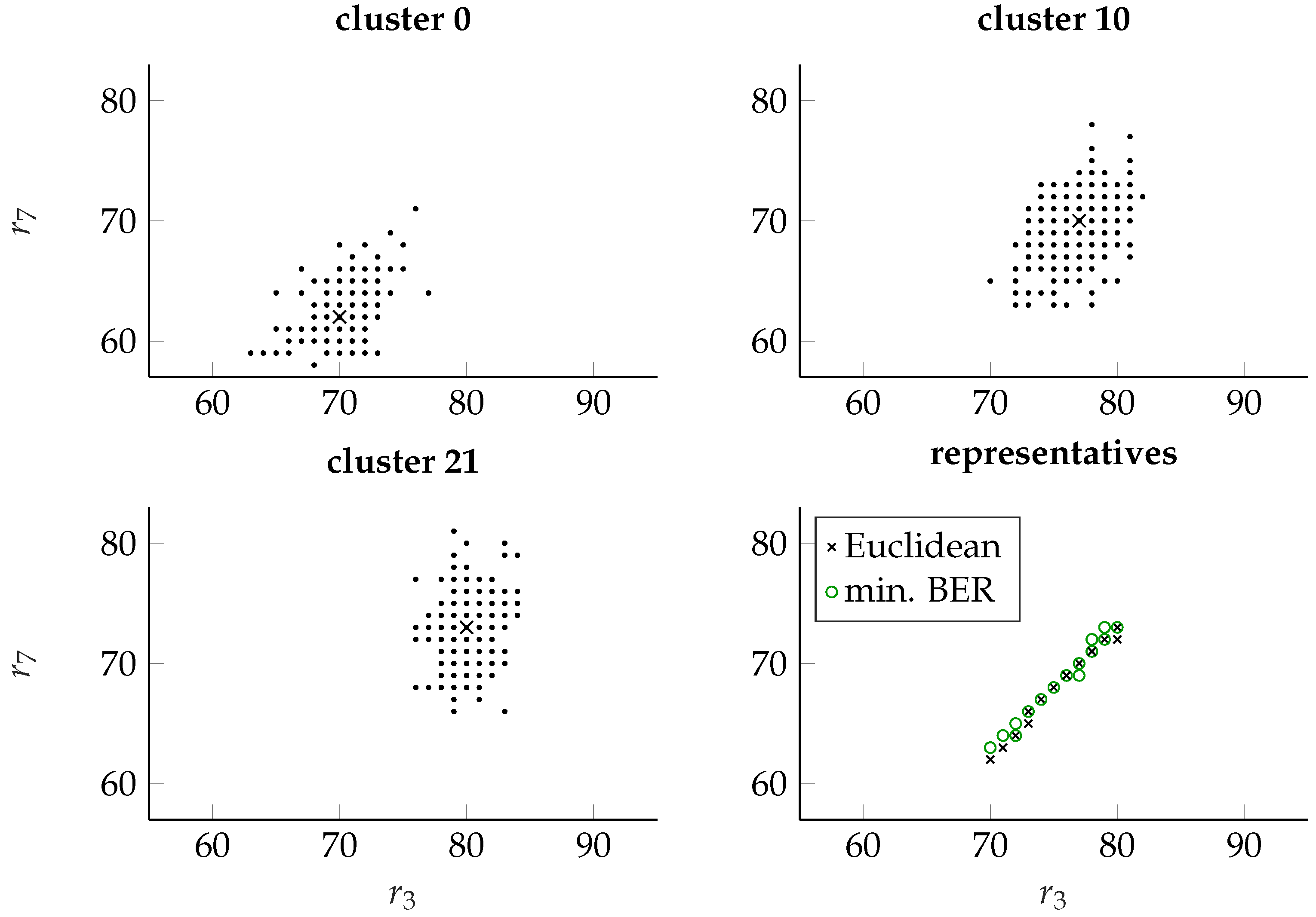
Figure 9 shows the clusters for 0, 10, and 21 errors in the meta-data of the MSB page. The MSB page is defined by references
and
. In the figures the optimum threshold voltage for the reference
is plotted versus the optimum threshold for reference
. Each point depicts a possible pair of optimal voltages that was observed for a given number of errors in the meta-data. The small crosses in the plots for the three clusters, indicate the representatives of the clusters. As can be seen in
Figure 9, the clusters are not well separated. This results from the small number of bits in the meta-data (
), which leads to a high variance in the number of errors.
The lower right-hand figure shows the representatives of all clusters obtained by minimizing the Euclidean distance or by minimizing the mean bit error rate (BER) in the cluster, respectively. We observe that both ways to determine the representatives achieve similar results. Since the
is typically lower than the
(cf.
Figure 7), a higher error count leads to larger predicted threshold voltage of the representative.
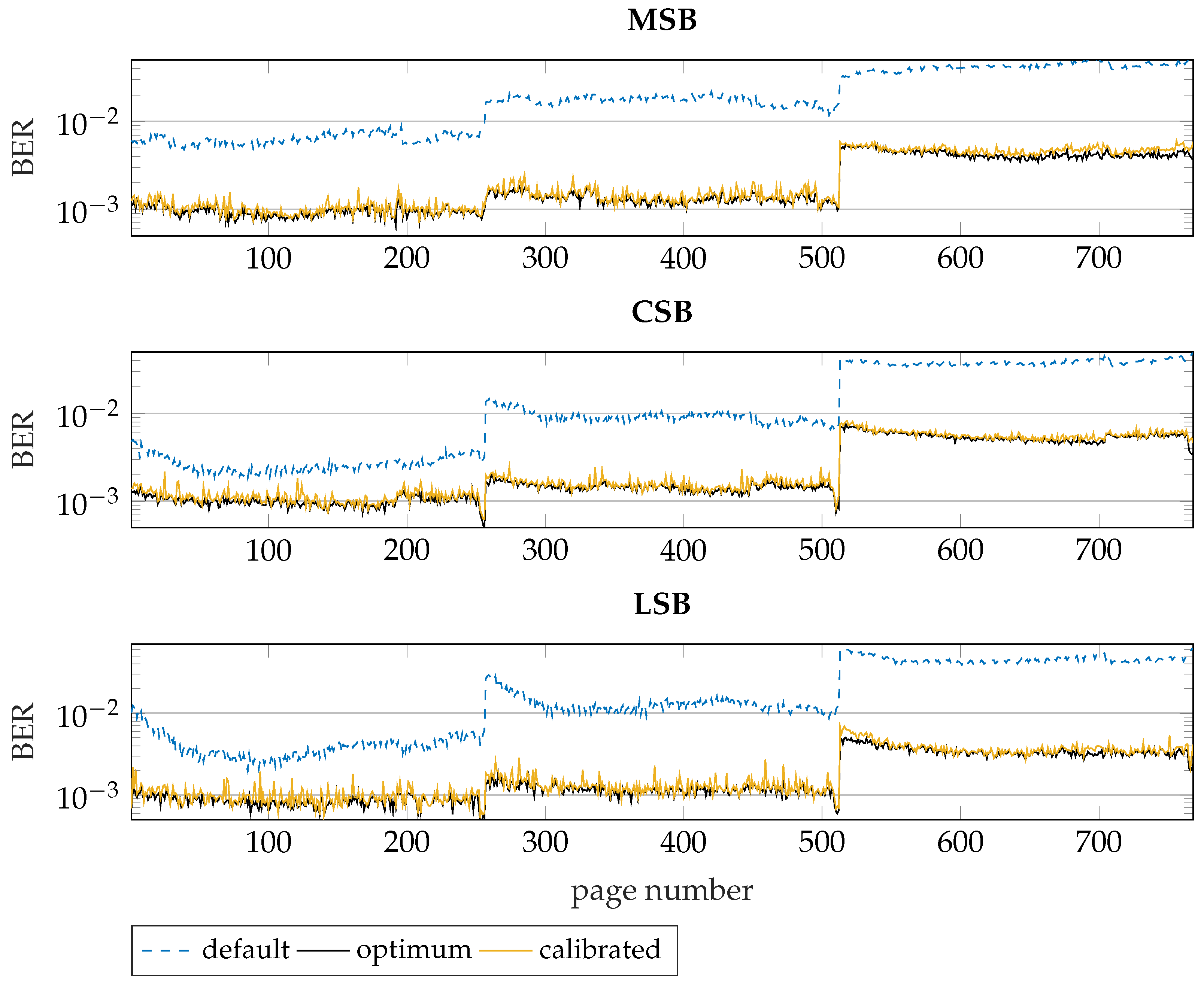
Figure 10 shows the results of this calibration procedure for three different life-cycle states. The x-axis shows the page number and the y-axis the bit error rate (BER) when reading at the default threshold voltage, the optimum threshold voltage for each page, and the calibrated threshold voltage. Each data set consists of 256 pages; the page numbers from 1 to 256 correspond to 1500 P/E cycles and 13 h baking; the pages from 257 to 512 consider 1500 P/E cycles and 80 h baking; the last 256 pages correspond to 3000 P/E cycles and 80 h of baking (EOL). The default threshold voltage is constant and only suitable for fresh flash memories, which is not shown in this figure because typically no calibration is required. The optimum threshold voltage is calculated for each page individually using the measurements.
While the calibration typically does not result in the optimum threshold voltage for each page, the BER is very close to the minimum possible error rate. Hence, this method provides a sufficiently precise calibration. On the other hand, it requires up to two times reading the meta-data and up to three times changing the threshold voltage, which leads to a relatively high overall latency.
Next, we analyze the impact of the calibration on the error correction performance. For this discussion, we consider a regular LDPC code of rate
and with a dimension
, i.e., the code is designed for 2kByte user data. For decoding, we consider the decoder proposed in [
45]. With soft-input decoding using three soft-bits (five read voltages for each reference), the decoder achieves a frame error rate (FER) of less than
for bit error rates below
. With hard-input decoding, the FER value of
is achieved at a BER value of 0.0038.
For the EOL case, the minimum BER without calibration is about . This error rate is above the error correction capability of the decoder even with soft-input decoding. With calibration, on the other hand, the maximum observed BER values among all pages in the EOL data is about . Hence, a frame error rate (FER) of less than is achieved with calibration even in the worst-case condition. Thus, for end-of-life conditions, calibration is required to reduce the probability of decoding failures.
However, reading soft information is extremely time-intensive. Consequently, it is interesting whether soft-decoding is required or hard-input decoding is sufficient. For a BER of
, the hard-input decoding results in a FER of about
, which is unacceptable. Hence, those cases definitively require soft-reading. Consider for instance the first life-cycle state shown in
Figure 10. Note that for about
of the pages, the BER is higher than
without calibration. With calibration, on the other hand, the highest BER in the first life-cycle state is about
, which leads to a FER lower than
with hard-input decoding. Hence, for pages with mid-life conditions, the calibration reduces the number of pages, which require soft-reading. This reduces the read latency and the power consumption for the read operation and the decoding.
In the next section, we discuss a tracking approach which reduces the latency for the threshold adaption of the remaining pages of a block.
5. Tracking the Read Threshold
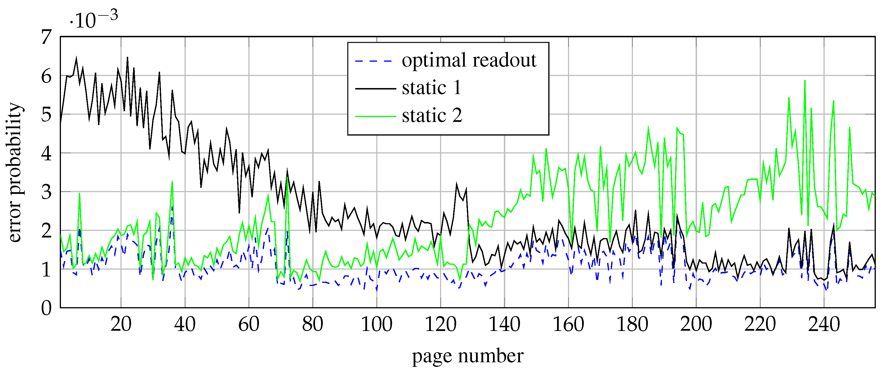
As described before, each page of a flash block has a specific readout threshold voltage
at which the lowest number of errors is observed. Unfortunately, these voltages may vary from page to page of the same block even when all pages have the same life-cycle condition, as shown in
Figure 11.
This figure illustrates the error probability for each page of a single TLC block at reference
with 3000 P/E-cycles and 55 h of baking. Note that the error rate at reference
is not equal to the BER of the MSB page because the MSB page uses references
and
(cf.
Figure 1). In
Figure 11, the curve labeled by
optimal readout indicates the smallest possible error probability for each page using the individual
values. The two other curves correspond to two static threshold voltages. For the curve
static 1, the threshold voltage was calibrated to the end of the block and for curve 2, the threshold voltage was calibrated to the beginning of the block. We observe that the static threshold voltages lead to significantly higher bit error rates.
The previous example shows that constant reference voltages for a complete black can cause a considerable performance degradation. To cope with this problem, we propose a tracking procedure for the reference voltages for consecutive pages. We assume that the calibration algorithm determined a near-optimal threshold voltage for the first page of the block.
As shown in
Figure 4, the optimal threshold voltage corresponds to a balanced error probability for 1-to-0 errors and 0-to-1 errors. The binary variable
A indicates the direction of the asymmetry between 0-errors and 1-errors.
indicates more 1-to-0 errors and
indicates more 0-to-1 errors. Hence,
A also provides the direction for the voltage change toward the equilibrium of the error probabilities.
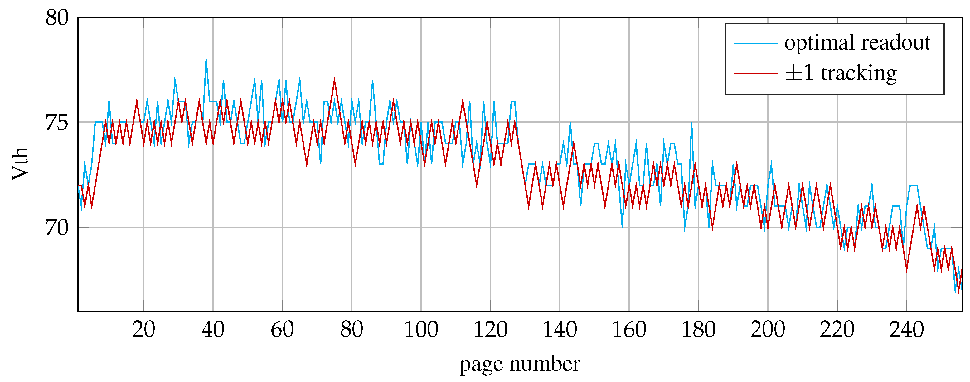
A simple approach for the tracking adapts the threshold voltage for the next page by a
voltage step depending on
A. This concept is illustrated in
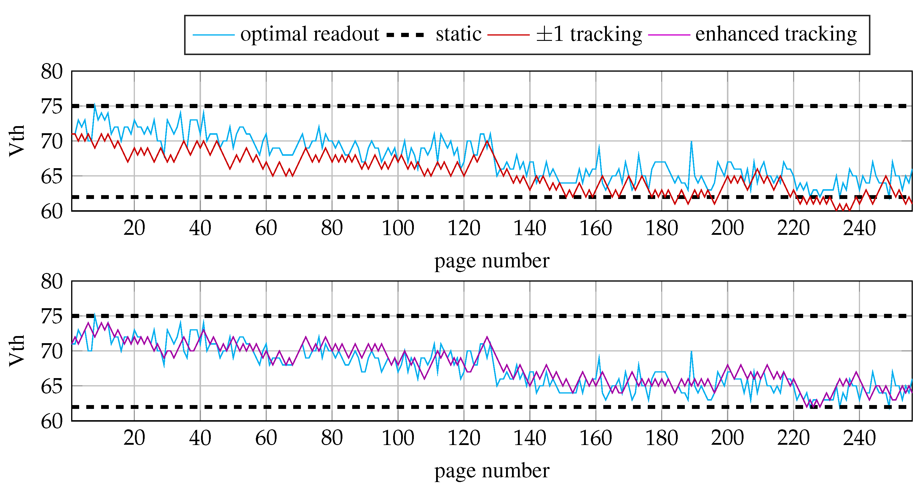
Figure 12. This figure depicts the adaptation of the threshold voltages over one block for reference
. The blue line shows the values of
for each page. The red curve presents the results with tracking, where
voltage steps are applied. We can observe that the adaptation follows the optimal voltage values.
The equilibrium of the error probabilities does not always coincide with
. This is indicated in
Figure 5 and
Figure 8. For instance, the equilibrium of the error probabilities corresponds to the value
in
Figure 5. In such a case, the tracking towards the equilibrium results in a bias, i.e., the estimated voltages systematically overestimate or underestimate
. This effect is displayed on the top part of
Figure 13. This figure shows the adaptation of the threshold voltages over one block for reference
. The dashed black lines correspond to the static voltages from
Figure 11, and the blue line shows the values of
for each page. The red curve depicts the results with tracking, where
voltage steps are applied. We can observe that the adaptation follows the optimal voltage values, but diverges slightly from the optimal curve, where
is mostly underestimated. On average, the bias corresponds to the shift
of the equilibrium.
In such a case, an enhanced tracking algorithm can be applied that corrects this bias. Instead of changing the value of
A at the equilibrium of the error probabilities, we calculate the rate of error number corresponding to the optimal voltage
or the shift
, respectively. For instance, in
Figure 5 the number of 1-to-0 errors is about 4-times the number of 0-to-1 errors. In this case, we can choose the value if
A such that
indicates four times more 1-to-0 errors then 0-to-1 errors. To average the ratio over different life-cycle states, we choose the ratio that corresponds to the value
for the mutual information
. The lower part of
Figure 13 shows the adjusted readout voltage with this approach. Now the adaptation is closer to the optimal voltage
.
Figure 12 and
Figure 13 show results for one block in a single life-cycle state.
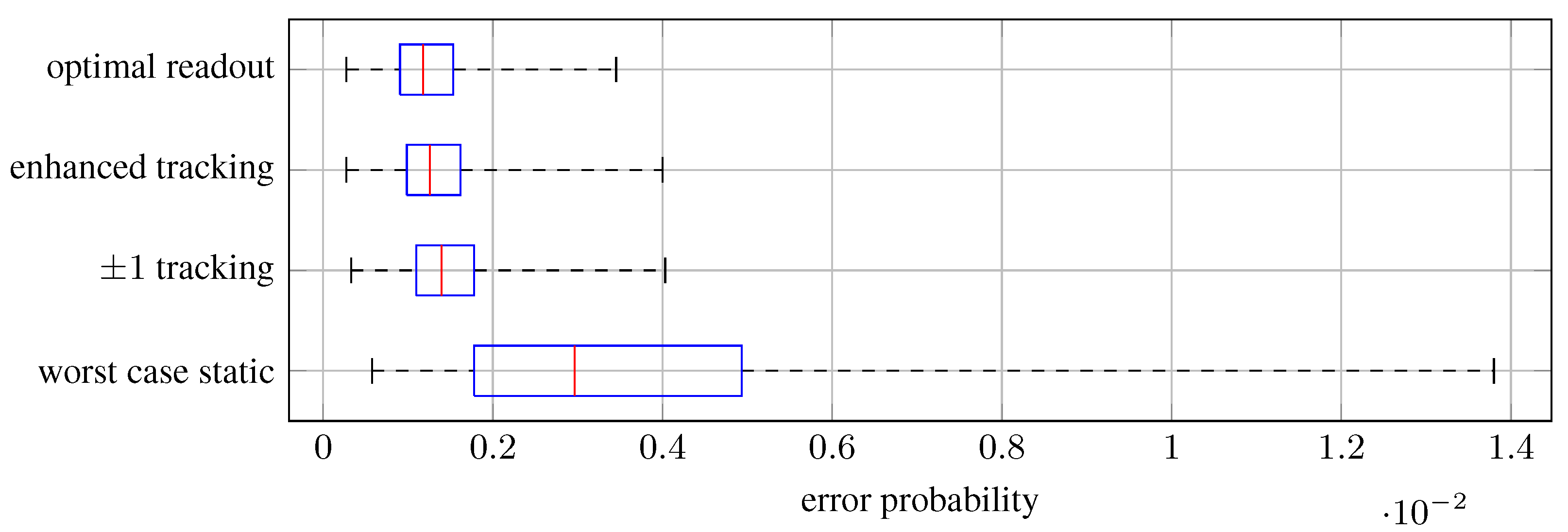
Figure 14 demonstrates the tracking accuracy averaged over different life-cycle states. In this box plot, the median of the error probability at
is represented as the central marker and a box represents the interquartile range, i.e., the interval for 50% of all measurements when ordered from lowest-to-highest error probability. The whiskers represent the most extreme data points without outliers.
The box plots consider the simple
voltage adaptation, the enhanced adaptation, and the worst-case static readout voltages. For every block in the data set, the worst-case readout voltage was selected within the range of optimal readout voltages. Hence, these values correspond to an optimal readout voltage of one page within a block, which was selected as static readout voltage for the entire block. The results in
Figure 14 show that a static readout voltage can significantly increase the error probability compared with the optimal voltage.
Again, we consider the LDPC code used in
Section 4 for the discussion of the ECC performance. We discuss results for the FER using hard-input decoding. For a BER of
, the hard-input decoding results in a FER of about
. Therefore, we assume that a soft-read operation is required for all BER values greater or equal
. For the worst-case static readout voltage, a significant amount of pages exceed the BER of
. When using the tracking approach the maximum BER is about
, which results in a FER of less than
with hard-input decoding. Consequently, the tracking improves the latency and the power consumption by reducing the profitability of soft-read and soft-input decoding procedures.
The
adaptation and the enhanced adaptation obtain a similar performance which is close to the optimal read voltage. Consequently, the bias compensation is not critical with respect to the achievable error rate. However, the bias compensation may be required for soft-input decoding [
15,
22]. Many soft-input decoding algorithms assume quantization intervals that maximize the mutual information between the input and output of flash memory, which requires an accurate voltage adaptation.


