
Two-Stage Clock-Free Time-to-Digital Converter Based on Vernier and Tapped Delay Lines in FPGA Device


Abstract
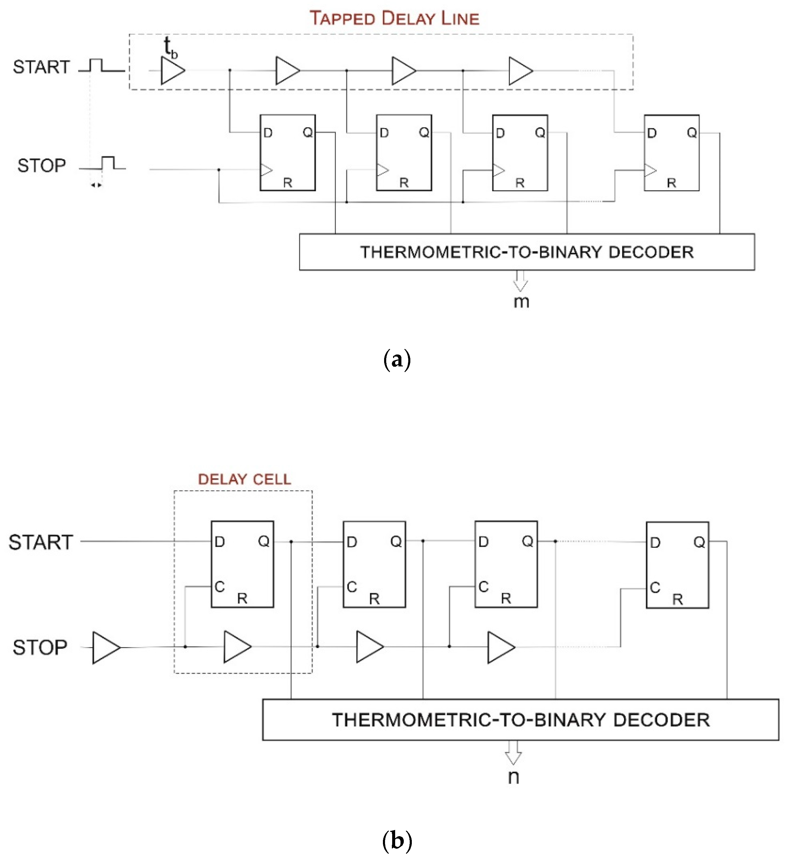
:1. Introduction
2. Method
3. Design and FPGA-Based Implementation
4. Results and TDC Parameters
5. Conclusions
Author Contributions
Funding
Conflicts of Interest
References
- Jansson, J.-P.; Koskinen, V.; Mäntyniemi, A.; Kostamovaara, J. A Multichannel High-Precision CMOS Time-to-Digital Converter for Laser-Scanner-Based Perception Systems. IEEE Trans. Instrum. Meas. 2012, 61, 2581–2590. [Google Scholar] [CrossRef]
- Maamoun, M.; Arami, S.; Beguenane, R.; Benbelkacem, A.; Meraghni, A. A 3 ps Resolution Time-to-digital Converter in Low-cost FPGA for Laser Rangefinder. In Proceedings of the World Congress on Engineering 2017 (WCE), London, UK, 5–7 July 2017; Volume 1. [Google Scholar]
- Russo, S.; Petra, N.; De Caro, D.; Barbarino, G.; Strollo, A.G.M. A 41ps ASIC time-to-digital converter for physics experiments. Nucl. Instrum. Methods Phys. Res. Sect. A Accel. Spectrometers Detect. Assoc. Equip. 2011, 659, 422–427. [Google Scholar] [CrossRef]
- Neiser, A.; Adamczewski-Musch, J.; Hoek, M.; Koenig, W.; Korcyl, G.; Linev, S.; Maier, L.; Michel, J.; Palka, M.; Penschuck, M.; et al. TRB3: A 264 channel high precision TDC platform and its applications. J. Instrum. 2013, 8, C12043. [Google Scholar] [CrossRef]
- Aidala, C.; Arrington, J.; Ayuso, C.; Bowen, B.; Bowen, M.; Bowling, K.; Brown, A.; Brown, C.; Byrd, R.; Carlisle, R.; et al. The SeaQuest spectrometer at Fermilab. Nucl. Instrum. Methods Phys. Res. Sect. A Accel. Spectrometers Detect. Assoc. Equip. 2019, 930, 49–63. [Google Scholar] [CrossRef] [Green Version]
- Swann, B.K.; Blalock, B.J.; Clonts, L.G.; Binkley, D.M.; Rochelle, J.M.; Breeding, E.; Baldwin, K.M. A 100-ps time-resolution CMOS time-to-digital converter for positron emission tomography imaging applications. IEEE J. Solid-State Circuits 2004, 39, 1839–1852. [Google Scholar] [CrossRef]
- Hong, K.J.; Kim, E.; Yeom, J.Y.; Olcott, P.D.; Levin, C.S. FPGA-Based Time-to-Digital Converter for Time-of-Flight PET Detector. In Proceedings of the 2012 IEEE Nuclear Science Symposium and Medical Imaging Conference Record (NSS/MIC), Anaheim, CA, USA, 29 October–3 November 2012; pp. 2463–2465. [Google Scholar]
- Nissinen, I.; Nissinen, J.; Holma, J.; Kostamovaara, J. A TDC-Based 4 × 128 CMOS SPAD Array for Time-Gated Raman Spectroscopy. In Proceedings of the ESSCIRC 2014—40th European Solid State Circuits Conference (ESSCIRC), Venice Lido, Italy, 22–26 September 2014; pp. 139–142. [Google Scholar]
- Karadamoglou, K.; Paschalidis, N.; Sarris, E.; Stamatopoulos, N.; Kottaras, G.; Paschalidis, V. An 11-bit High-Resolution and Adjustable-Range CMOS Time-to-Digital Converter for Space Science Instruments. IEEE J. Solid-State Circuits 2004, 39, 214–222. [Google Scholar] [CrossRef]
- Karadamoglou, K.; Paschalidis, N.; Stamatopoulos, N.; Kottaras, G.; Paschalidis, V.; Sarris, E. A 32 Bit, High Resolution, Asynchronous Time to Digital Converter for Space Instruments. In Proceedings of the 2004 IEEE Aerospace Conference Proceedings (IEEE Cat. No.04TH8720), Big Sky, MT, USA, 6–13 March 2004; Volume 4, pp. 2398–2403. [Google Scholar]
- Szplet, R. Time-to-Digital Converters. In Design, Modeling and Testing of Data Converters; Springer: Berlin/Heidelberg, Germany, 2014; pp. 211–246. [Google Scholar]
- Nutt, R. Digital Time Intervalometer. Rev. Sci. Instrum. 1968, 39, 1342. [Google Scholar] [CrossRef]
- Szymanowski, R.; Kalisz, J. Integrated Time Counter with 200 Ps Resolution. In Proceedings of the Norchip Conference, Oslo, Norway, 8–9 November 2004; pp. 207–210. [Google Scholar]
- Jansson, J.-P.; Mäntyniemi, A.; Kostamovaara, J. A CMOS Time-to-Digital Converter with Better Than 10 ps Single-Shot Precision. IEEE J. Solid-State Circuits 2006, 41, 1286–1296. [Google Scholar] [CrossRef]
- Staszewski, R.; Leipold, D.; Hung, C.-M.; Balsara, P. TDC-Based Frequency Synthesizer for Wireless Applications. In Proceedings of the 2004 IEE Radio Frequency Integrated Circuits (RFIC) Systems, Forth Worth, TX, USA, 6–8 June 2004; pp. 215–218. [Google Scholar]
- Tsai, T.-H.; Yuan, M.-S.; Chang, C.-H.; Liao, C.-C.; Li, C.-C.; Staszewski, R. A 1.22ps Integrated-Jitter 0.25-to-4GHz Fractional-N ADPLL in 16nm FinFET CM0S. Dig. Tech. Pap. IEEE Int. Solid State Circuits Conf. 2015, 58, 260–261. [Google Scholar] [CrossRef]
- Bogdan, M.; Frisch, H.; Heintz, M.; Paramonov, A.; Sanders, H.; Chappa, S.; DeMaat, R.; Klein, R.; Miao, T.; Wilson, P.; et al. A 96-channel FPGA-based Time-to-Digital Converter (TDC) and fast trigger processor module with multi-hit capability and pipeline. Nucl. Instrum. Methods Phys. Res. Sect. A Accel. Spectrometers Detect. Assoc. Equip. 2005, 554, 444–457. [Google Scholar] [CrossRef] [Green Version]
- Arpin, L.; Bergeron, M.; Tetrault, M.-A.; LeComte, R.; Fontaine, R. A Sub-Nanosecond Time Interval Detection System Using FPGA Embedded I/O Resources. IEEE Trans. Nucl. Sci. 2010, 57, 519–524. [Google Scholar] [CrossRef]
- Arabul, E. A Precise High Count-Rate Multi-Channel Coincidence Counting Instrument for Quantum Photonics Applications. Ph.D. Thesis, The University of Bristol, Bristol, UK, September 2020. [Google Scholar]
- Szplet, R.; Jachna, Z.; Kwiatkowski, P.; Różyc, K. A 2.9 ps equivalent resolution interpolating time counter based on multiple independent coding lines. Meas. Sci. Technol. 2013, 24, 035904. [Google Scholar] [CrossRef]
- Mantyniemi, A.; Rahkonen, T.; Kostamovaara, J. A CMOS Time-to-Digital Converter (TDC) Based on a Cyclic Time Domain Successive Approximation Interpolation Method. IEEE J. Solid-State Circuits 2009, 44, 3067–3078. [Google Scholar] [CrossRef]
- Szplet, R.; Kwiatkowski, P.; Jachna, Z.; Różyc, K. An Eight-Channel 4.5-ps Precision Timestamps-Based Time Interval Counter in FPGA Chip. IEEE Trans. Instrum. Meas. 2016, 65, 2088–2100. [Google Scholar] [CrossRef]
- Dudek, P.; Szczepanski, S.; Hatfield, J. A high-resolution CMOS time-to-digital converter utilizing a Vernier delay line. IEEE J. Solid-State Circuits 2000, 35, 240–247. [Google Scholar] [CrossRef]
- Aloisio, A.; Branchini, P.; Cicalese, R.; Giordano, R.; Izzo, V.; Loffredo, S. FPGA Implementation of a High-Resolution Time-to-Digital Converter. In Proceedings of the 2007 IEEE Nuclear Science Symposium Conference Record, Forth Worth, TX, USA, 6–8 June 2004. [Google Scholar] [CrossRef]
- Xilinx Inc. Vivado Design Suite User Guide: Using Constraints; User Guide, UG903; Xilinx Inc.: San Jose, CA, USA, 2018. [Google Scholar]
- Balla, A.; Beretta, M.M.; Ciambrone, P.; Gatta, M.; Gonnella, F.; Iafolla, L.; Mascolo, M.; Messi, R.; Moricciani, D.; Riondino, D. The characterization and application of a low resource FPGA-based time to digital converter. Nucl. Instrum. Methods Phys. Res. Sect. A Accel. Spectrometers Detect. Assoc. Equip. 2014, 739, 75–82. [Google Scholar] [CrossRef]
- Szplet, R.; Kalisz, J.; Jachna, Z. A 45 ps time digitizer with a two-phase clock and dual-edge two-stage interpolation in a field programmable gate array device. Meas. Sci. Technol. 2009, 20, 025108. [Google Scholar] [CrossRef]
- Cova, S.; Bertolaccini, M. Differential linearity testing and precision calibration of multichannel time sorters. Nucl. Instrum. Methods 1970, 77, 269–276. [Google Scholar] [CrossRef]
- Sondej, D.; Szymanowski, R.; Szplet, R. Methods for Determining Equivalent Transfer Characteristic of Precision Time-to-Digital Converter with Discrete Delay Line. Metrol. Meas. Syst. 2021, 28, 4. [Google Scholar]
- Wu, J.; Shi, Z. The 10-Ps Wave Union TDC: Improving FPGA TDC Resolution beyond Its Cell Delay. In Proceedings of the 2008 IEEE Nuclear Science Symposium Conference Record, Dresden, Germany, 19–25 October 2008; pp. 3440–3446. [Google Scholar]
- Chaberski, D.; Frankowski, R.; Gurski, M.; Zieliński, M. Comparison of Interpolators Used for Time-Interval Measurement Systems Based on Multiple-Tapped Delay Line. Metrol. Meas. Syst. 2017, 24, 401–412. [Google Scholar] [CrossRef]
- Kwiatkowski, P. Employing FPGA DSP Blocks for Time-to-Digital Conversion. Metrol. Meas. Syst. 2019, 26, 631–643. [Google Scholar] [CrossRef]


| Utility | Low Resource TDC (Resolution 625 ps) [26] | Classical Two-Stage TDC (Resolution 45 ps) [27] | Proposed Two-Stage TDC (Resolution 13 ps) |
|---|---|---|---|
| Slice registers | 61 | 238 | 169 |
| Slice LUTs | 24 | 215 | 183 |
| BUFG | ≥4 | 7 | 0 |
| Parameter | Value (ns) |
|---|---|
| Mean of predictors | 1.8 |
| Mean of observations | 1.89 |
| Intercept | 0.28 |
| Slope | 0.89 |
| Regression equation | y = 0.89x + 0.28 |
| RMSE | 0.104 |
Publisher’s Note: MDPI stays neutral with regard to jurisdictional claims in published maps and institutional affiliations. |
© 2021 by the authors. Licensee MDPI, Basel, Switzerland. This article is an open access article distributed under the terms and conditions of the Creative Commons Attribution (CC BY) license (https://creativecommons.org/licenses/by/4.0/).
Share and Cite
Szplet, R.; Czuba, A. Two-Stage Clock-Free Time-to-Digital Converter Based on Vernier and Tapped Delay Lines in FPGA Device. Electronics 2021, 10, 2190. https://doi.org/10.3390/electronics10182190
Szplet R, Czuba A. Two-Stage Clock-Free Time-to-Digital Converter Based on Vernier and Tapped Delay Lines in FPGA Device. Electronics. 2021; 10(18):2190. https://doi.org/10.3390/electronics10182190
Chicago/Turabian StyleSzplet, Ryszard, and Arkadiusz Czuba. 2021. "Two-Stage Clock-Free Time-to-Digital Converter Based on Vernier and Tapped Delay Lines in FPGA Device" Electronics 10, no. 18: 2190. https://doi.org/10.3390/electronics10182190
APA StyleSzplet, R., & Czuba, A. (2021). Two-Stage Clock-Free Time-to-Digital Converter Based on Vernier and Tapped Delay Lines in FPGA Device. Electronics, 10(18), 2190. https://doi.org/10.3390/electronics10182190