1. Introduction
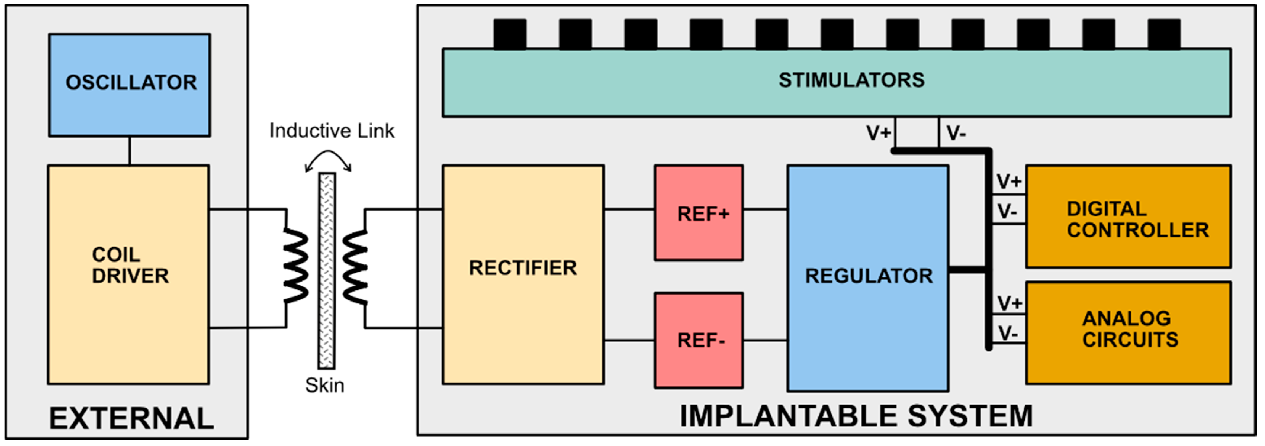
A block diagram of the bio-implantable system is shown in
Figure 1. The external system comprises a coil driver, which wirelessly transmits power to the implanted system. The transmitted power enables the operation of an implantable system comprising a rectifier, reference circuit, low dropout regulator (LDO), digital controllers, analog circuits, and stimulators. The reference circuit is the first block after the rectifier, and the entire system relies on the robustness of the reference circuit. The DC voltage is generated by passing through a rectifier and LDO from an AC power signal, which is wirelessly transmitted via an inductive link [
1,
2] or infrared radiation [
3]. However, the misalignment of the inductively coupled coils or the infrared source sometimes reduces the power transmission efficiency. Consequently, the implanted rectifier produces an unstable output voltage ripple, which is then fed to the input terminal of the reference circuit. Therefore, the voltage reference circuit must provide a stable output over the device process, power supply, and temperature variations. Significant works on reference circuit design have been reported in the literature [
4,
5,
6,
7,
8,
9], where attempts were made to reduce the variations in the voltage owing to temperature variations. In detail, the prior methods were based on compensating the negative temperature coefficient of a diode-connected bipolar junction transistor (BJT) or complementary metal-oxide semiconductor (CMOS) with a positive temperature coefficient thermal voltage.
The temperature compensation, termed the curvature-compensation technique, of a first-order or higher-order nonlinear voltage or current is often limited by the operating supply voltage. Channel length modulation also occurs in the transistor when the supply voltage increases. A cascode current mirror, which enables high output impedance, was commonly used in earlier studies to suppress the channel length modulation effect. However, at high supply voltages, a phenomenon called impact ionization in metal-oxide semiconductor (MOS) transistors creates a leakage current to the substrate that causes problems in the cascode current mirror [
10].
The voltage across the drain-depletion region and drain current change the magnitude of the substrate current. This is because the drain to the substrate parasitic resistance is created (for the NMOS) in parallel with the output impedance of the MOS transistor. Thus, as the supply increases, the parasitic resistance dominates and significantly reduces the total impedance of the cascode current mirror. This effect produces a significant error in the distributing current to all branches, including the temperature compensation circuits. Consequently, the temperature compensation circuits depend on the supply voltage. Increasing the supply voltage could produce errors in the voltage or current that severely impact the line sensitivity of the reference circuit. Furthermore, these conventional methods require additional circuitry to sink the undesirable current out of the output branch or to add current to the output to compensate for the output voltage variations [
11,
12,
13,
14], resulting in an expansive layout footprint and higher power consumption. Accordingly, the typical compensation technique for voltage reference is unsuitable for implantable devices. Since our body maintains a constant temperature of 37 °C, it is essential for bio-implantable applications to increase the line regulation efficiency and decrease power dissipation rather than temperature compensation.
Motivated by this, we propose a novel reference circuit optimized for implantable devices that uses nonlinear current compensation circuits to increase the power line regulation performance and power supply rejection ratio (PSRR). The proposed reference circuit was designed using a standard SK-Hynix 0.35 μm CMOS standard process.
The current paper extends our previous work in [
15]. Our previous work focused on a positive reference only, which was used in LDO to generate a positive supply voltage. However, a negative supply in the stimulators (shown in
Figure 1) is also needed to generate balanced biphasic pulses. Therefore, additional circuits, such as a charge pump circuit or inverting voltage circuit, were required in the previous work to generate the negative voltage, increasing the design’s total area, due to additional components such as capacitors. The new circuit in this paper fulfils this requirement by having positive and negative references. Furthermore, it utilizes simple compensation circuits to produce excellent performance in PSRR and line regulation for positive and negative reference voltages.
2. Methods
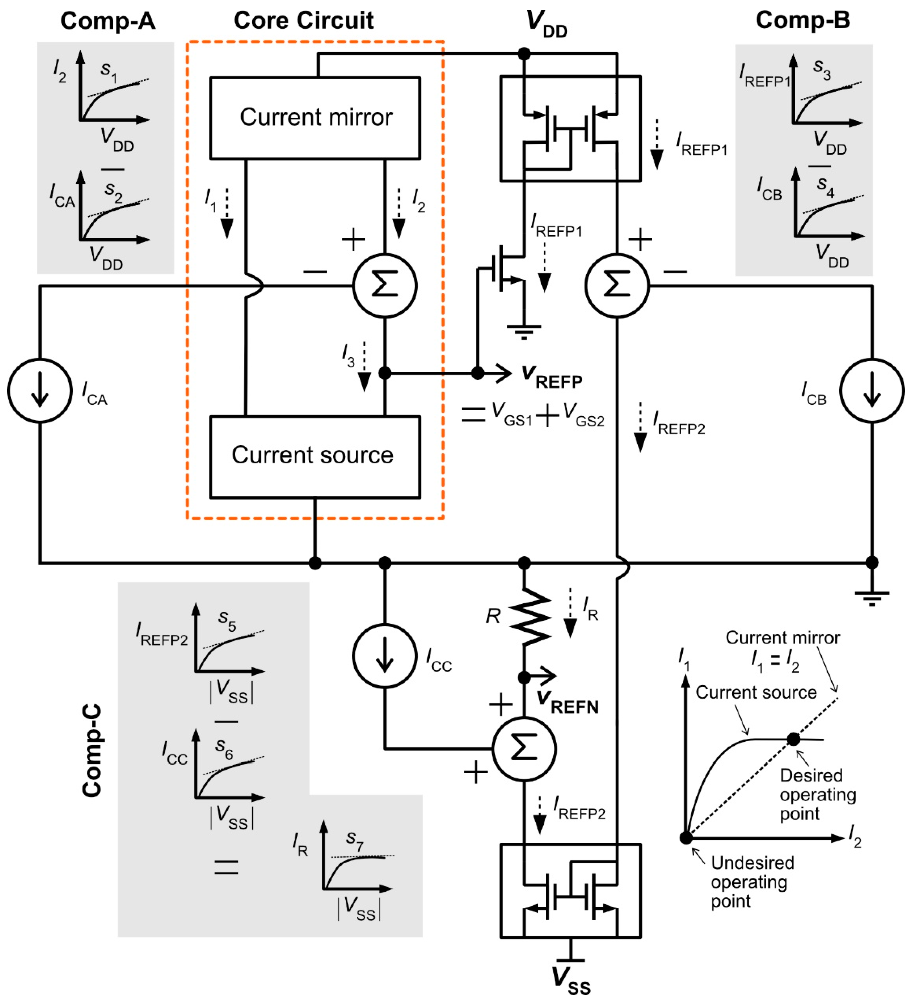
The proposed reference circuit diagram is illustrated in
Figure 2. The core circuit is based on a self-biasing gate-source voltage reference [
6]. The positive reference voltage,
VREFP, is the established voltage across the current source circuit when both the current mirror and current source in the core circuit reach the desired operating point, as shown in
Figure 2. However, an undesired operating point should be avoided because
I1 =
I2 = 0, a start-up circuit guarantees that the proposed circuit is not trapped in the zero-current state by initiating a current in the core circuit. The summation of
VGS1 and
VGS2 from
produces
VREFP. The negative reference voltage,
VREFN, indicates the voltage generated when
IR flows into the resistor,
R. The three compensation circuits devised in this work are designated as Comp-A, Comp-B, and Comp-C in
Figure 2.
Comp-A and Comp-B aim at alleviating the supply-dependent current in
I2 and
IREFP1, leaving a constant current in the core and current mirror circuits. A constant current can be achieved by equalizing the slopes of
S1 and
S2, as well as those of
S3 and
S4, respectively, for Comp-A and Comp-B. Comp-C generates the current
ICC, which is added to the current mirror circuit. Assuming that
ICC and
IREFP2 are linear currents, they may be written as
where
ICC_DC and
IREFP2_DC are the DC currents of
ICC and
IREFP2, respectively. If
S5 =
S6,
ICC in Equation (1) can be written as
The current through resistor the
R is given by
Substituting Equations (2) and (3) into Equation (4) gives:
Equation (5) suggests that an independent supply current
IR (
S7 = 0) is obtained if
S5 =
S6 (the detailed equations are provided in
Appendix A). The PSRR performance is also increased by incorporating Comp-A, Comp-B, and Comp-C into the proposed circuit. The small-signal analysis that proves this idea will be presented later.
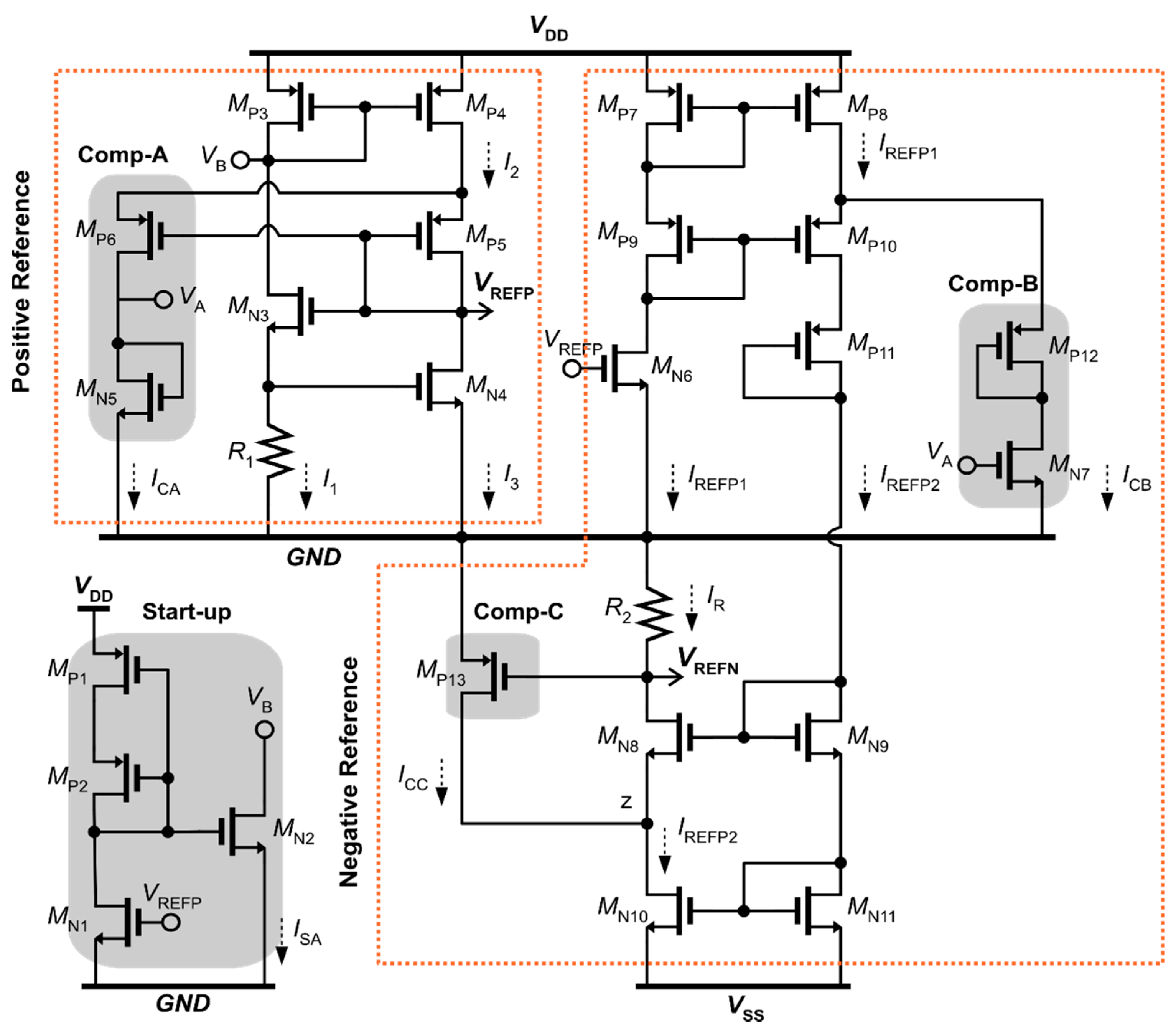
Figure 3 illustrates the proposed dual-voltage reference circuit based on the circuit diagram shown in
Figure 2. When the supply is powered up, the start-up circuit sinks some current through
MN2, denoted as
ISA, which then initiates a voltage at the gate terminals of
MP3 and
MP4. The current starts flowing through
MP3 and
MP4, thereby establishing
VREFP. When
VREFP exceeds the threshold voltage of
MN1, current flows through
MP1 and
MP2. The decrease in voltage at the drain terminal of
MN1 moves
MN1 into a deep triode region and eventually leads
MN2 to operate in a cut-off region.
MP6,
MP5,
MP12,
MN7, and
MP13 are newly added to the proposed reference circuit that consists of the Comp-A, Comp-B, and Comp-C circuits presented in
Figure 2. The slopes of
S2,
S4, and
S6 shown in
Figure 2 can be adjusted by varying the size of transistors
MP6,
MN7, and
MP13, respectively, as shown in
Figure 3.
VREFP can be obtained from the circuit as:
MN6,
MP7, and
MP9 form a current reference circuit, providing
IREFP1 to
MP8. The nonlinear current in
IREFP1 is compensated by Comp-B, resulting in
IREFP2, which is mirrored by
MN10. The constant current
IR produces
VREFN across
R2, given as:
Since VREFN becomes more negative if IR increases, the source-gate voltage of MP13 increases and more current flows into MP13. According to Equation (5), the increment in ICC decreases IR. Thus, the negative feedback loop returns VREFN back to its initial value.
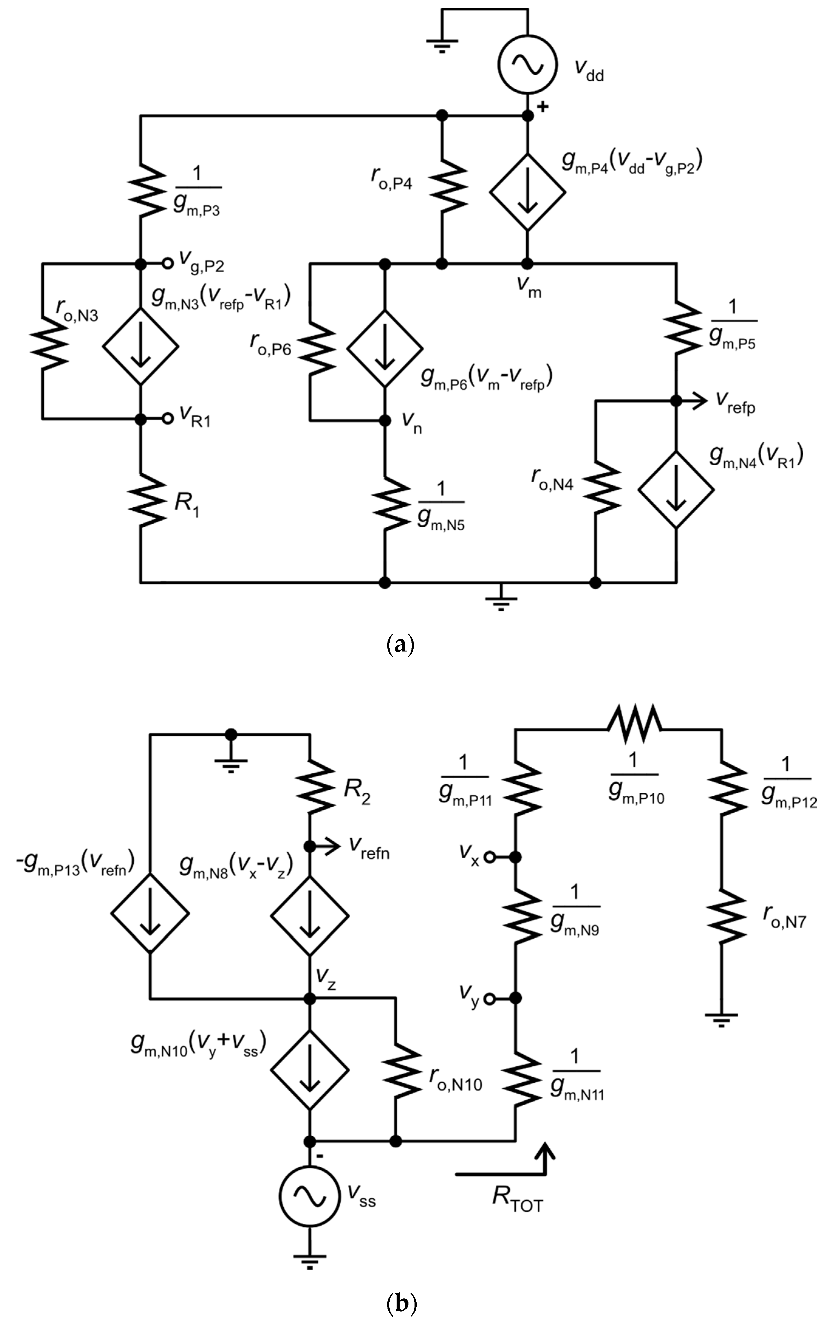
Figure 4a shows the equivalent circuit for the positive reference (
VREFP) small-signal analysis.
vR1 can be approximately equal to
vrefp because it is the output of the source follower circuit formed by
MN3 and
R1 in
Figure 3. Therefore,
vg,P2 can be obtained by letting
After rearranging Equation (8) for
vg,P2, we obtain
, resulting in
. Applying nodal analysis at the node of
vm, the following equation can be derived:
Assuming that
and
are large, Equation (9) can be simplified as
Here,
can be derived from the circuit written as
Substituting Equation (11) into Equation (10),
vrefp/
vdd can be obtained as follows:
Mathematical analysis shows that exhibits small variations with . in Equation (12) ensures that the ratio of vrefp/vdd is nearly zero. The proposed Comp-A contributes in Equation (12), and hence increases the PSRR performance.
A small-signal analysis of the negative reference is illustrated in
Figure 4b. The signal path through
MP10 and
MP8 is ignored because
IREFP1 is assumed to be an ideal current source. Assuming
, respectively, the
ro of
MP13 and
MN8 can be neglected. From
Figure 4b, the total resistance,
RTOT, is extremely high, owing to
ro,N7; hence, we can assume that
, resulting in
. Applying nodal analysis at the node of
vZ, the following equation is obtained:
and
Substituting Equation (14) into Equation (13) and rearranging for
vrefn/
vss, we can obtain Equation (15).
Equation (15) indicates that vrefn/vss is inversely proportional to ro,N10. In addition, ro,N10 is increased by a factor of gm,p13R2, introduced by Comp-C, which decreases the ratio vrefn/vss. gm,p13 can be further increased by increasing ICC; however, IR will be reduced slightly, causing VREFN to become more positive. Hence, the PSRR is limited by the minimum value of VREFN.
The positive and negative reference voltages are fed into the LDO. Thus, PSRR in the LDO is influenced by the reference circuit. The PSRR performance of the LDO also includes an open-loop gain of the error amplifier and output capacitor. In practice, the reference voltage rejects supply noise at a low-frequency region only; hence a high PSRR reference at low frequency is required. The error amplifier maintains a high PSRR in the middle region until it reaches a 3-dB roll-off frequency. The output capacitor of the LDO determines the high-frequency PSRR performance.
Table 1 tabulates the component parameters used for the proposed dual-voltage reference circuit.
3. Results
The proposed reference circuit was verified using a Hynix 0.35 μm CMOS standard process. As shown in
Figure 5a,
VGS,N4 decreases, whereas
VGS,N3 increases with increasing
VDD. As
ICA in Comp-A increases rapidly at higher
VDD,
VREFP decreases. Thus, the slope of
VGS,N3 is assigned to be more positive than 3.5 mV/V to compensate for the variations at higher
VDD.
MN7 in Comp-B senses the variations in
VDD and produces
ICB, as shown in
Figure 5a, which compensates for the current variation in
IREFP1. The slope of
ICB (
S4 in
Figure 2) can be adjusted by varying the size of
MN7. Comp-C tracks the changes in voltage at node
z, as shown in
Figure 3, and produces
ICC, which varies in the same manner as
IREFP2, owing to channel-length modulation.
ICC and
IREFP2 vary from 10 µA to 19 µA and 15.7 µA to 24.7 µA, respectively, and consequently, a stable
IR of 5.7 µA is obtained when
VSS ranges from 2.8 V to 12 V.
The variations in output voltage with respect to
VDD and
VSS are presented in
Figure 5b. For bio-implantable applications, that is, retinal prosthetics, it is crucial to generate a negative supply voltage for producing a cathodic waveform in a biphasic pulse [
14]. Accordingly, we observed a negative output reference voltage with a supply dependency of 1.583 mV/V. As shown in
Figure 5a, the nonlinear
ICC increases in a similar fashion to
ICA; however,
VGS,N3 compensates for the
VREFP variation caused by
ICA. Conversely,
VREFN varies at a high supply voltage owing to unmatched current rate changes in
ICC and
IREFP2. Thus, the negative reference line regulation is larger than the positive reference line regulation (0.916 mV/V).
The elaborate corner results for line regulation are shown in
Figure 5c, according to which the compensation circuits proposed in this work can generate stable reference voltages in various environments. Furthermore, the positive and negative PSRR results with respect to
VDD and
VSS are plotted in
Figure 5d, where the maximum PSRRs of −112 and −128 dB were obtained for
VREFP and
VREFN, respectively. The PSRR difference between
VREFP and
VREFN arises from the different factors in the denominator;
ro,P4 in Equation (12) increases by a factor of
gm,N4(
gm,p5 +
gm,p6), while
ro,N10 in Equation (15) increases by approximately
gm,P13.
Finally, the overall performance of the proposed reference is tabulated in
Table 2 and compared with the previous voltage reference circuits presented in [
12,
13,
16]. The line regulation obtained was higher than those in [
13,
16], but lower than that in [
12]. However, the proposed reference circuit exhibits excellent PSRR compared with [
12,
13,
16]. The voltage range was 9.2 V, close to [
13], while the corresponding quantities for [
12,
16] were 3 V and 0.5 V, respectively, indicating that the proposed work is robust to wide supply changes. Considering the accuracy and stability, the proposed reference circuit with excellent line regulation and PSRR is suitable for a wide supply and high precision LDO. In addition, the proposed negative reference could possibly replace the charge pump circuit, which is typically used to generate negative voltage.


