1. Introduction
Information is treated as the most valuable asset in present day since about billions of items of information are processed and shared per second in this technological world. This large amount of information must be processed and shared in a very secure manner. Since information is treated as a most valuable thing, there is also a very high chance of piracy or alteration of this information by an unintended user [
1,
2,
3,
4,
5]. Unauthorized change and availability of the original information also form the major goal of the researchers to keep the information secure. Researchers use cryptographic algorithms to keep information secret while transmitting and receiving information on an insecure channel. Cryptographic algorithms perform encryption operations on the original plain text before transmitting and perform decryption operation after receiving the encrypted text from the insecure channel. A secret key is used for both encryption and decryption operations. Based on the usage of a number of secret keys, cryptographic algorithms can be classified as symmetric and asymmetric algorithms. Furthermore, algorithms can be classified as block and stream cipher algorithms based on the number of bits, and the algorithms can operate simultaneously [
6,
7,
8,
9,
10]. Generally, these cryptographic algorithms are utilized in different applications such as banking applications, military and government [
11], and critical infrastructures such as Smart Grid [
12,
13].
In 2001, the National Institute of Standards and Technology (NIST) published a symmetric algorithm called AES which is a replacement of the data encryption standard (DES) [
14,
15]. AES is one of the extensively used symmetric key cryptography algorithm that uses same key for both the encryption and decryption of the sensitive data [
16,
17]. In the last two decades, researchers have developed many cryptographic efficient algorithms. Still, AES stands as the most secure cryptographic algorithm due to its cost effectiveness and easier implementation in both hardware and software. AES is a non-Feistel cipher that has the same rounds of operations in both the encryption and decryption processes. It is being proved that hardware implementations of the AES is more secure and faster than that of software implementations [
18,
19,
20,
21]. The AES is categorized as AES-128, AES-192 and AES-256 based on the length of the key. Here, the 128, 192, and 256 indicates the length of the key used during the cryptographic process [
22]. A high-performance modern microprocessors are used to design the AES for satisfying the high throughput requirements in the desired applications. However, a VLSI based hardware description language (HDL) design of AES is accomplished to obtain the low silicon area and high speed [
23]. An architectural modification such as pipelining, subpipelining, and loop-unrolling are used to enhance the throughput and operational frequency [
24,
25]. A high-speed AES design is obtained by using the hardware architectures with unwound loops and pipelines. However, this architecture faces the high area consumption while accomplishing the encryption operation [
26].
The traditional symmetric/asymmetric algorithms are used for the data security such as DES [
27,
28,
29], triple DES [
30], elliptic curve cryptography (ECC) [
31,
32,
33,
34], Rivest–Shamir–Adleman (RSA) [
35], etc. In these algorithms, ECC and RSA are well known asymmetric-key-cryptography that use public keys for encryption/decryption processes. In the conventional general-purpose processors, the conventional cryptographic algorithms obtain less speed and demands higher resources during the computation process [
36]. For example, the RSA has a complex design and low-level efficiency, and hence it is not appropriate for low-area applications [
37]. Nowadays, some of the block ciphers from the symmetric algorithms are also used for the data security purpose and examples of the block cipher are SIMON [
38], SEED [
39], KLEIN [
40], HIGHT [
41], KASUMI [
42], CLEFIA [
43], PRESENT [
44,
45], etc. These low complexity light weight block ciphers can be used in wireless communications (i.e., internet of things (IoT) applications). If the number of devices in the certain communication increases, then it creates difficult issues such as higher hardware utilization and delay. Therefore, theses block ciphers aren’t suitable for the low area applications [
46].
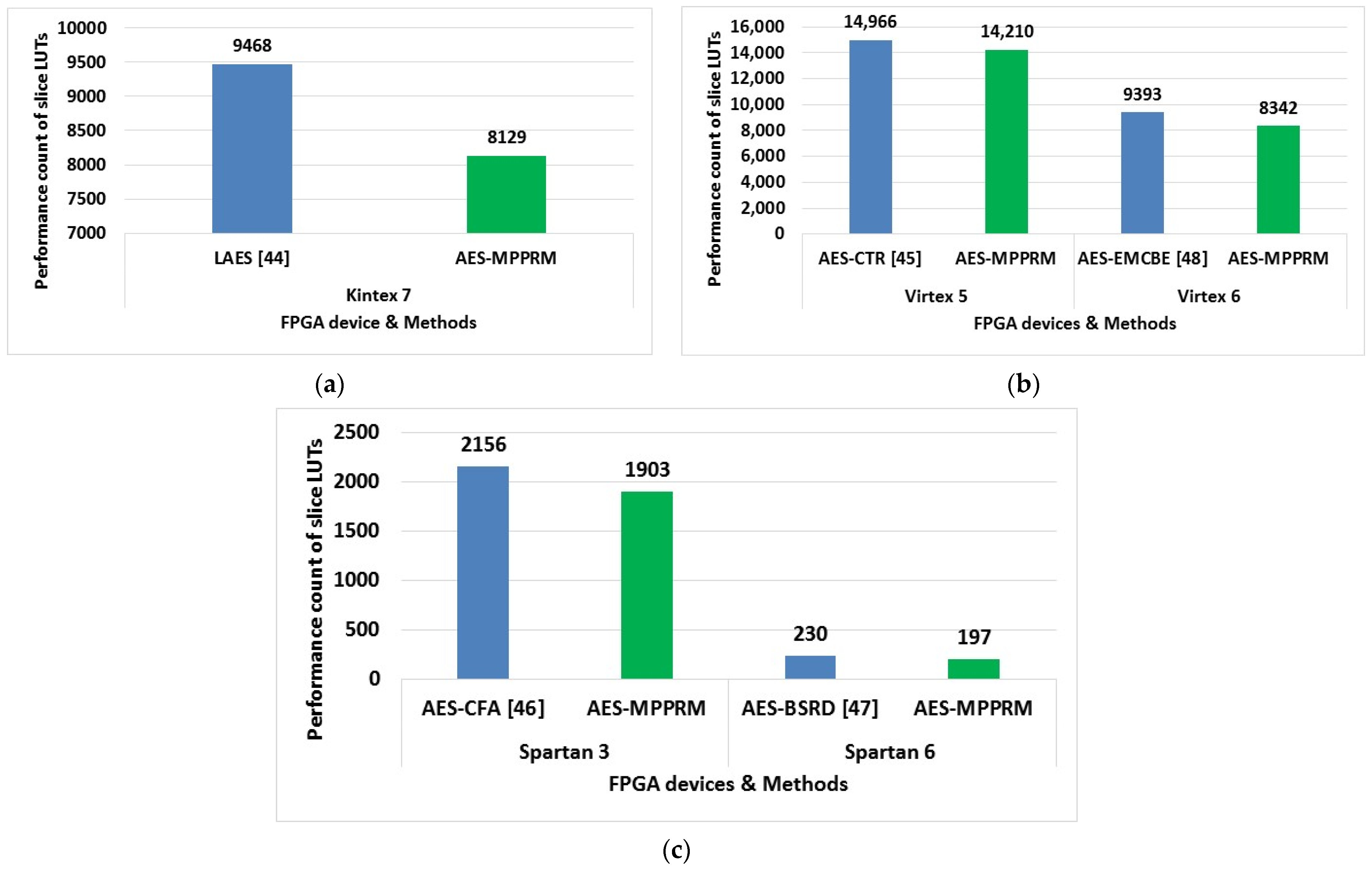
Kumar, K et al. [
47] presented the design of lightweight AES (LAES) algorithm in Artix-7 and Kintex-7 FPGAs to secure the voice data. The operation of the mix column was decreased in the LAES algorithm than the conventional AES algorithm. After decreasing the operations of the mix column, the 128-bit cipher text was acquired from the results of shift rows operation. The reduction in the mix column process was resulted in the less delay as well as it was used to minimize the logic operation. Therefore, the complexity of this LAES algorithm was decreased while encrypting the voice data. However, the reduction in the mix column was increased the utilization of the multiplexers. Shahbazi, K. and Ko, S.B [
48] developed the high throughput FPGA design of AES algorithm in counter (CTR) mode on Xilinx Virtex-5 for high traffic applications. In this work, the AES was modified based on the following two strategies: (1) sub-bytes and shift-rows were exchanged for the first nine rounds, and (2) the shift rows were combined with added round keys. Here, the inner pipelining, outer pipelining, and loop-unrolling were used for obtaining a higher throughput. A new-affine-transformation, which was a combination of inverse isomorphic and affine transformation, was used to minimize the area of the Sub-Bytes. Moreover, the operation of the mix-column was separated into two stages for obtaining an equal latency among the stages. However, the execution of the mix column operation in on clock cycle was resulted in higher latency.
Arul Murugan, C et al. [
49] presented iterative architecture of AES-128 encryption for enhancing the security. The LUT was used in the composite field arithmetic (CFA) to perform the multiplication in the S-box. Subsequently, the area was minimized by using the updated architecture of the S-box in the AES. Additionally, the Vedic multiplier was used in the operation of mix columns for minimizing the hardware resources of the AES. Here, three different FPGA devices such as Virtex-4, Virtex-5, and Spartan 3 devices were used to design the AES algorithm. The utilization of the CFA resulted in higher speeds in the process of sub-byte transformation. However, the architecture of the mix column transformation was highly complex when compared to the architecture of the shift-row transformation. Wegener, F et al. [
50] developed the extended version of the AES in Spartan 6 for compromising the requirements of area and latency. The Bit-Serial Rotational Design (BSRD) was used instead of the S-box in the AES architecture. Moreover, the nonlinear proportion was significantly decreased by using the rotational symmetry technique for implementing the S-box of the AES algorithm. The linear operation was replicated and executed independently in the AES algorithm, which increased its area.
Madhavapandian and Maruthu Pandi [
51] presented the design of secure architecture for the Transmission Control Protocol/Internet Protocol (TCP/IP). The protection over the TCP/IP protocol was achieved by using the 128 bit of AES algorithm. Next, the AES architecture was optimized for reducing the power consumption and cost. Moreover, an improved compressed structure for the mix columns was used along with the efficient mix column Boolean expression (EMCBE) for optimizing the structure of the AES. Here, the AES algorithm was designed and implemented using the Virtex 6 algorithm. However, the technique of gate replacement used for minimizing the delay affected the scalability of this AES architecture. Zodpe and Sapkal [
52] developed the pseudo-random noise (PN) sequence generator for generating the values of the S-box. The distinct sequence of random numbers was generated by using the PN generator based on the feedback taps and initial seed value. An efficiency of the cryptosystem was improved based on the features of the PN sequence generator. Here, the requirement for applying the external key was avoided by using an initial key generation technique. However, the utilization of hardware resources of the AES was high, when it was designed by using the non-pipelined stages.
Sikka et al. [
53] presented the high throughput FPGA implementation for the AES algorithm. Here, the AES algorithm was designed for the automotive applications. Specifically, the Vivado high-level synthesis (HLS) tool was used to design the AES with a 128-bit of key size and block size of 10 rounds. This HLS was used mainly based on the application-specific bit widths that used to design the FPGA. The implementation of AES using the HLS was used to improve the speed. However, the delay of this AES algorithm was increased because of the frequent re-calculation of the signal width for each input, output and intermediate value.
The existing methods are analyzed and explained as follows: for a better implementation of the AES, the hardware resources (e.g., slices and LUT) are required less during the encryption/decryption process. But, the requirements of the multiplexers are increased, when mix column operation is minimized in the LAES [
47]. The replication of linear operation increases the area of the AES in encryption/decryption processes [
50]. Moreover, the hardware resources of the AES are improved when it is designed by using the non-pipelined stages [
52]. The latency is increased in the AES operation in the mix column operation [
48]. Next, the delay of the AES is increased due to the frequent re-calculation of the signal width [
53]. In order to overcome the aforementioned issues, an MPPRM based SubBytes transformation is designed to reduce the hardware resources used during the encryption/decryption process. Additionally, the delay element added in the AND gate of the MPPRM is used to minimize the delay caused in the encryption process.
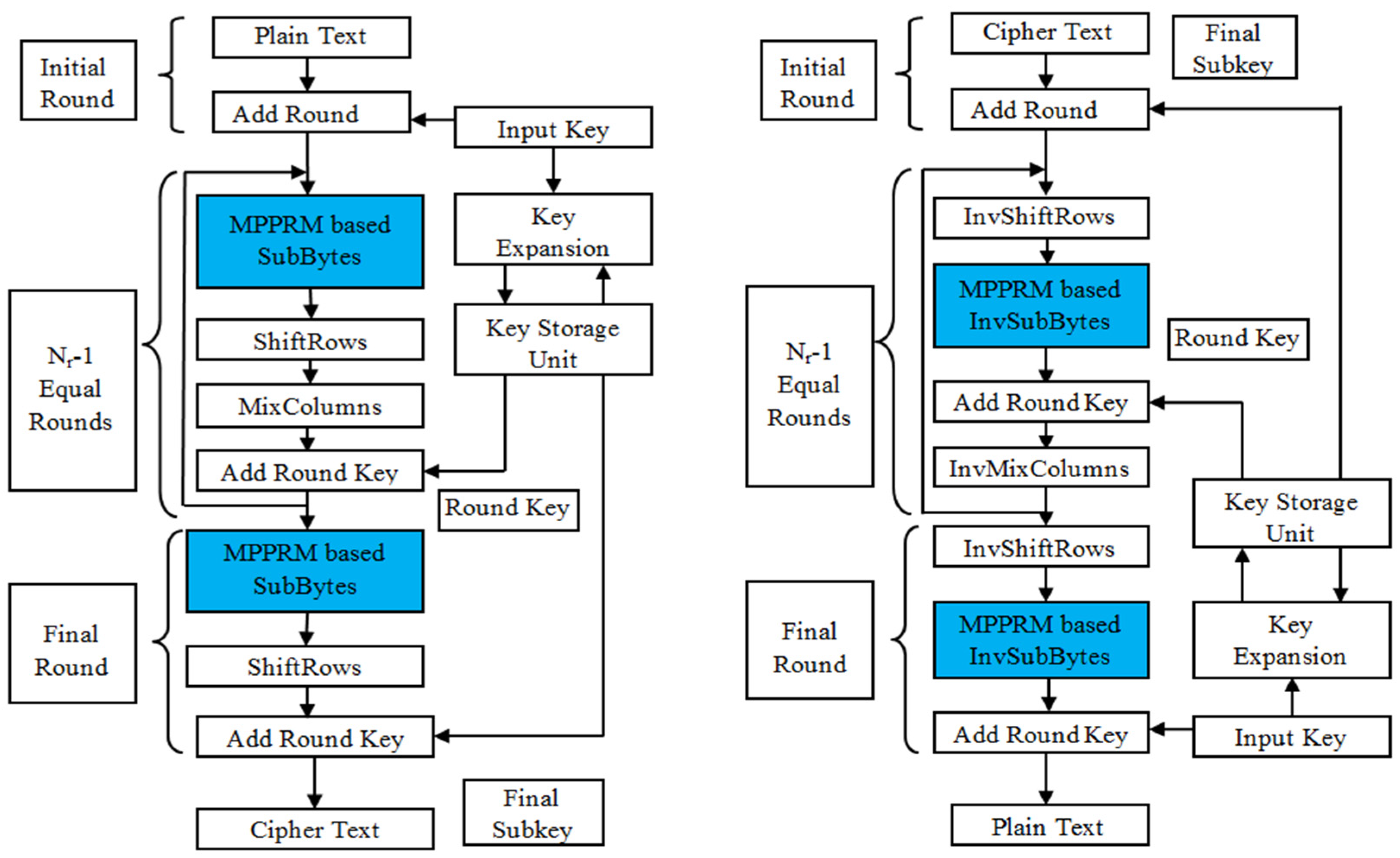
Generally, the SubBytes transformation processed in the AES is considered as bottleneck during the encryption process, since the transformation calculates the most resource demanding multiplicative inverse function at the finite field arithmetic operation. The SubBytes transformation designed by using the read only memory creates an inappropriate delay in the AES encryption/decryption [
54]. From the modifications of pipelining, subpipelining, and loop-unrolling, the subpipelining is used to achieve maximum speed with minimal area occupancy. LUT based approaches used in the SubBytes and InvSubBytes transformation stages causes much delay than the total delay of all of the other transformations. Therefore, in this work LUT based transformation is replaced with the minimal delay combinational circuits. Composite field architecture is one such architecture that provides the required logics. Also, composite field arithmetic structure has been implemented with subpipelinining architecture in this work. However, delays can also be reduced by eliminating the delays occurring due to dynamic hazards that take place in combination circuits. This is achieved by implementing SubBytes and InvSubBytes transformation in MPPRM architecture. Here, both the architectures are explored and hardware utilization comparisons are made to explore the most suitable architecture. Algorithms used for secure communication must withstand the cryptanalytic attacks which aim to find the secret key based on the techniques and mathematical operations used in converting plain text to cipher text. With the aim of optimizing the AES structure, a MPPRM based SubBytes transformation is accomplished for achieving the less area and lesser hardware resources during the FPGA implementation.
The most important contributions of this research work are given as follows:
This work uses composite field arithmetic structure both SubBytes and InvSubBytes transformations with the speed efficient subpiplining structure. Earlier approach of implementing CFA is to decompose GF(28) as GF(((22)2)2). Where in this work GF(28) is decomposed as GF((24)2).
MPPRM architecture is used for both SubBytes and InvSubBytes transformations for minimizing the AND and XOR gates to minimize the hardware resources used in the encryption/decryption process.
In this work, key expansion architecture is used to provide 128-bit key for subpipelined structure. A speed efficient AES-MPPRM architecture is achieved, because of the delay element added in the AND gate output.
The organization of the paper is given as follows: The information about the conventional AES algorithm is provided in
Section 2.
Section 3 provides the detailed explanation about the AES-MPPRM architecture. The modified new architecture in key expansion module is detailed in
Section 4.
Section 5 gives the results and discussion of the AES-MPPRM architecture. The conclusion of this research paper is provided in
Section 6.
2. Related Works
The information about the conventional AES encryption and decryption process is provided in this section. This section contains the process of substitution, shift rows, mix columns, added round keys, key expansion architecture, subpipelined architecture, and composite field arithmetic operation.
2.1. AES Algorithm
Advanced encryption standard (AES) is a symmetric cryptographic algorithm, in which a single secret key is used for both encryption and decryption operations. AES has three different versions and each version operates at different bit levels of secret key. Based on the number of bits in the secret key, AES can be classified as AES-128, AES-192, or AES-256. Number of rounds of encryption and decryption operation for each version also varies from one another and it is given in
Table 1.
Every round in the AES algorithm uses different subkeys, which are generated from the main original key. Although key sizes are different for each version, no of bits from the original data to be communicated securely remains same for all the versions. Data block size is 128 bits for all of the three versions of the AES algorithm. Number of rounds denotes the number of encryption operation takes places for a single data block with different subkeys obtained from the key expansion process. Diffusion and confusion process for each round remains same. Initially, the main key is utilized for pre round transformation and other subkeys are used in each round. So number of keys required will be always higher than the amount of rounds in AES versions.
2.2. AES Encryption and Decryption
AES is generally a non-Fiestel block cipher cryptographic algorithm that encrypts plain original text into encrypted cipher text with the help of secret key. Secret key lengths differ for different versions of the AES algorithm, as mentioned in
Table 1. The same algorithm which is utilized to transform the plain text into cipher text can also be used to get back the plain text from the cipher text by using a secret key used in the encryption process. Except for the last round in all of the AEs versions, all of the other rounds will have the following four operations in both the encryption and decryption processes. Before proceeding to the encryption process, 128-bit plain text is grouped into a state matrix of order 4 × 4 with each element in the matrix is represented as a word (2 bytes).
2.2.1. Substitution Transformation
Substitution is a process in which a byte value is replaced by another byte. Only non-linear process involved in the AES algorithm is substitution.
Each byte in the state matrix is considered as a polynomial in the Galois Field 28. Next, the affine transformation and matrix multiplication are used to transform the byte. Substitution can also be conducted directly using the RijndaelS-box. In decryption, inverse S-box is used for the substitution process. Substitution step introduces the actual confusion to the original data, forms the important step in preserving the original data from unauthorized access.
2.2.2. Shift Rows
The rows of state array are periodically shifted in the shift row phase. Here, the second, third, and fourth rows are shifted left by one, two and, three times, respectively, where the first row remains unaffected in the given input. Moreover, the rows are shifted right for accomplishing the decryption operation. Shift row is the first process of diffusion in the AES algorithm. This shift row process is invertible.
2.2.3. Mix Column Transformation
Similar to the operation of the shift row, the mix column operation is carried out in the column level. Here, the matrix multiplication is used to perform the operation of the mix column. The mix column and inv mix column operation are expressed in the following Equations (1) and (2).
where
and
are the output obtained after mix column operation;
and
are the input for mix column operation obtained as the output of Shift row operation.
2.2.4. Add Round Key
The important operation in the AES algorithm is add round key, since all of the earlier three steps are invertible. Without this operation, AES encryption becomes meaningless. Function of secret key takes place at the add round key operation. In this operation the original secret key or several subkeys are first arranges as a state matrix of 4 × 4 order. Matrix addition between keys and plain text is the operation in the add round key. As a result of this add round key operation, we get the cipher text.
All the above four operations are repeated for n number of times, where n denotes the number of rounds in the AES version. For every iteration, a different subkey is used. Therefore, for n number of rounds, n number of subkeys must be derived. Derivation of several subkeys from single main secret key is referred as key expansion process. Operation in the key expansion process or key schedule process must be carefully implemented, since the relation between subkeys should not be exploited easily. The mathematical way is followed by the key expansion process for deriving the different keys from the single way. In AES-MPPRM architecture, the time consumption is minimized for obtaining the subkeys from main key.
2.3. Key Expansion Architecture
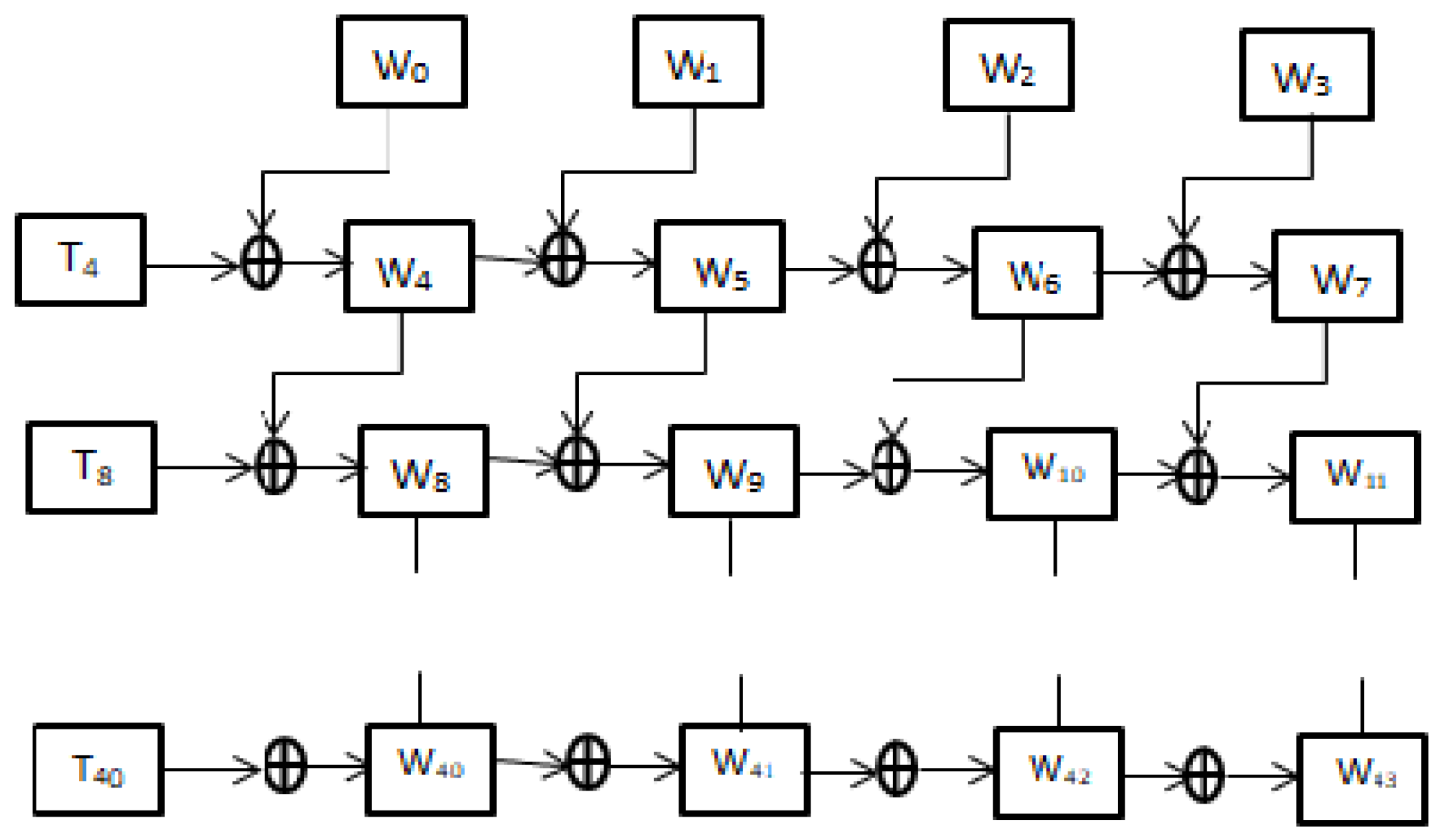
AES-128 key expansion process is discussed in this section. In the key expansion process, the main secret key of 128 bit is divided into four words, each with 32-bit length. For AES-128, 10 subkeys must be derived from main original secret key. These subkeys are used in process of producing cipher text from plain text.
Figure 1 clearly explains the process of key scheduling or key expansion. Mathematical operations are performed with the main key to derive the subkeys. Interdependency with the previous subkey makes the key expansion process efficient.
Mathematical operation takes place at the word level and consecutive four words are combined together to form a subkey. For example, W4, W5, W6, and W7 are combined to form first subkey. Key expansion algorithm generates a total of 4 (Nr + 1) words. Mathematical operation used here is just an EXOR operation between a previous word and a word from the previous subkey.
Generation of Temporary Word
Temporary word is the most important thing in key expansion process, since the only non-linear process involved in generation of subkeys is in the process of generation of temporary word. The first word of every subkey is generated as a result of EXOR operation between its corresponding temporary word and a word from a previous subkey. Three operations are performed in a word to create a temporary word. Substitution, Rotation and EXOR are the three operations which are performed in the process of creating a temporary word. For AES-128, temporary words are necessary to create W
4, W
8, W
12, W
16, W
20, W
24, W
28, W
32, W
36, W
40. Simply for i ≠ 4Nr, temporary words are not needed. Equation (3) represents the generation of the temporary word.
where, ‘i’ denotes the word number and ‘Nr’ denotes the round number in AES.
The rotword routine is identical to the Shift row routine, however it is used for the only one row. Moreover, the subword is similar to the Sub byte routine. The value of R constant differed for each round is provided in the
Table 2.
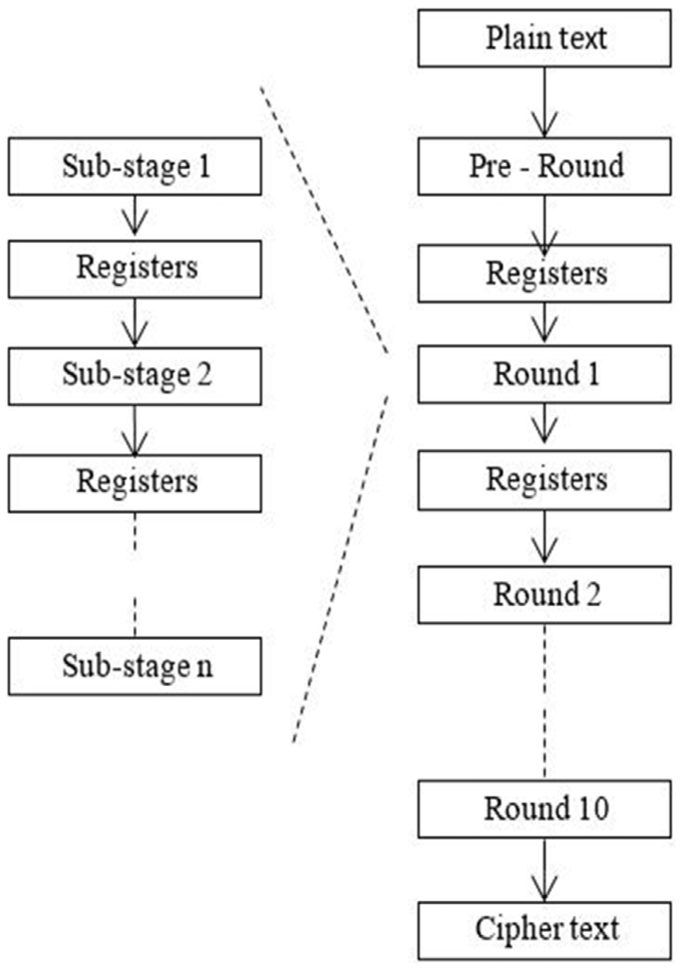
2.4. Subpipelined Architecture
As stated in the first section subpipelining architectural optimization achieves maximum speed and great throughput than that of pipelining and folded architectures. To implement subpipelining, approach registers are inserted between each stage of every round and registers are also inserted between the rounds to store the intermediate results. One of the main advantages of subpipelining over folder structures is that it can simultaneously operate multiple blocks of data. Subpipelining involves splitting each round of AES operation into n substages, as shown in
Figure 2. The total delay in each substages involves set up delay, propagation delay, multiplexer delay, and combinational circuits delay (which are very small). Here, each substages within a round are divided with equal delay, with extra registers included within and between the rounds adds up more area to the architecture. It is noted that when the number of substages with equal delay are increased for each round, improvement in speed can be achieved. But dividing the rounds into substages does not improve the speed of the architecture due to the delay caused by adding a greater number of registers. Some of the component of rounds may give minimal delay when compared to the delay provided by the substages of that component. This is entirely because of the accumulated delay due to the additional registers. In those cases it is better not to divide those components into substages. Although subpipelining makes the blocks to be processed simultaneously, the average number of clock cycles for processing a block remains same. This is also the reason for not dividing each round after particular parts. As we know that that individual logic gates delay is the highest undividable delay of any combinational logics in non LUT based design. Based on this result, rounds can be divided into substages.
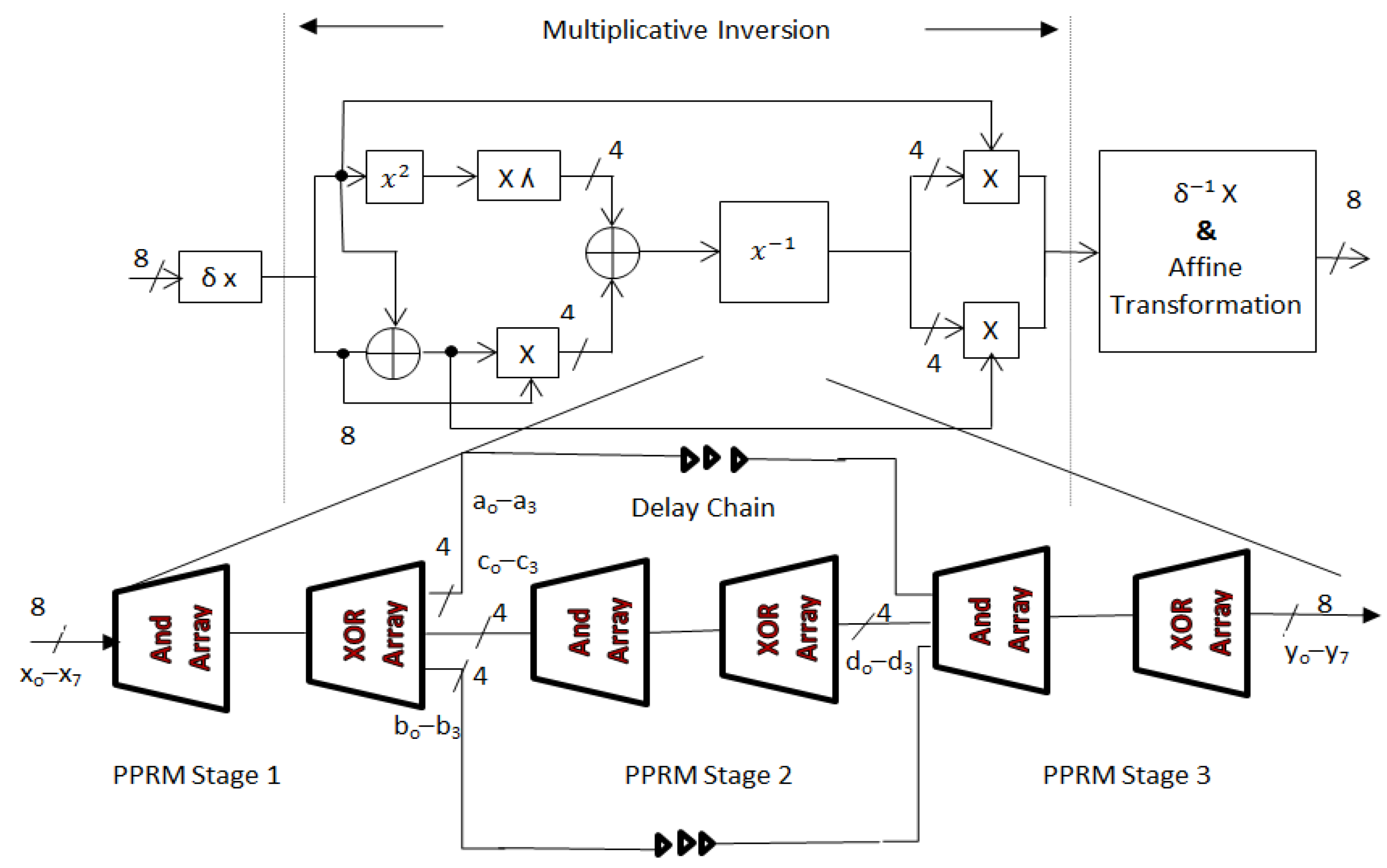
2.5. Composite Field Arithmetic
As stated in the previous section, composite field arithmetic is implemented to increase speed as well as throughput of the AES encyptor and AES decryptor. For SubByte transformation, a byte must undergo a multiplicative inversion process and affine transformation. Composite field arithmetic is used to find the multiplicative inverse of a byte without much complexity overload. CF is denoted as GF ((2n)m) and Gf (2k) is isomorphic to GF ((2n)m) when K = nm. It is employed by mapping lower order GF to higher order GF.
The GF (2
8) is built from mapping GF by using the Equation (4).
The values of ɸ and ʎ are chosen as 10 and 1100, respectively, to make the above three equations as an irreducible equation. Isomorphic mapping function f(
x) = δ ×
x and its inverse f(
x)
−1 are to be mapped to its composite field element and its inverse field element, where δ is a matrix with binary digits as its elements based on the GF (2
8) elements and its composite field elements. Suitable matrix for composite field and Galois field is expressed in the Equation (5).
Due to isomorphic mapping, transformation stages in an AES algorithm are not suited for composite field implementation. Mix column and inverse mix column transformation must be provided some modification to make it suitable for the subpipelining architecture. In mixcolumn operations, {02}16 and {03}16 are mapped to {5F}16 and {5E}16, respectively, whereas in inverse mixcolumn operation, {0d}16, {09}16, {0b}16, and {0e}16 are mapped to {09}16, {75}16, {2a}16, and {57}16, respectively, in the composite field. These modifications increase the hardware complexity on implementation of mixcolumn and inverse mixcolumn operations. In case of shift rows, Inverse Shift Rows and Key expansion stages operations are independent of Galios field representations. Therefore, no modifications are needed for these stages to implement Composite Field Arithmetic structure suitable for subpipelining architecture.


 ,
, 


