1. Introduction
Modern CMOS Image Sensors (CIS) devices are present everywhere, such as in cellphones, cameras, security systems, traffic devices and medical equipment, among many others. They can occur in the form of line-scan, area-scan and depths scanners, for visible light, infrared (NIR and LWIR), X-ray imaging, LiDAR, and so on. In this sense, CIS devices are used in the automotive field, in industrial applications and in the consumer’s market, as well as in various medical, scientific and space-related areas. Particularly in the industrial and scientific areas, the low-light noise, high dynamic-range, low power dissipation and speed are the main features of interest regarding CIS devices.
It is known that the thermal and the flicker noise sources are the main noise contributors in a CIS device, degrading the sensor’s electrical readout noise performance. However, the flicker noise is the noise source that limits device image quality the most in our modern era. Given this, this work presents an indirect way to reduce the significant flicker noise contribution, while keeping the thermal noise interference under control, preferably by reducing it even further. This is obtained by means of designing a fast high-order, low voltage supply, incremental sigma-delta converter so that the system can provide low noise output samples in a short period. An additional overview of the stacked technology is addressed in this paper, namely the overall picture regarding a future CIS implementation, where features such as low noise, low power and low temporal resolution are allowed at virtually any array spatial resolution, by employing 3D-stacked IC design techniques.
This paper expands and deepens the research works from the same authors, presented at the ICEA workshop in 2019 [
1], complemented with the research work published in the Sensors and Actuators (S&A) A: Physical Journal in the course of 2020 [
2], with the research paper published in the MDPI Electronics Journal published during 2021 [
3], in conjunction with the work published in the Microelectronics Journal during 2021 [
4]. All these works are concerned with high-order Incremental Signal-Delta (ISD) converters and a low-power design.
The rest of the paper is organized as follows:
Section 2 provides a background on the 3D-staking design subject, while
Section 3 provides background for contextualizing the reader with low-light imaging.
Section 4 focus on the problem at hand, addressing the issues of sub-electron low noise imaging while maintaining the competitiveness of the CIS devices.
Section 5 focuses on the proposed solutions one should adopt, based on the recent findings from related works, in which fast, low-noise and low power ADC circuits emerge, as part of the project’s main goal.
Section 6 mainly presents the electrical characteristics of the re-designed enhanced oversampling 3rd-order ISD converter, under quite realistic noise conditions.
Section 7 addresses the re-designed enhanced complete readout chain circuits, providing the equivalent system response and the noise floor under the most realistic power supplies environmental noise scenario. Lastly, the research work’s conclusions are drawn in
Section 8.
2. 3D-Stacked Technology Background
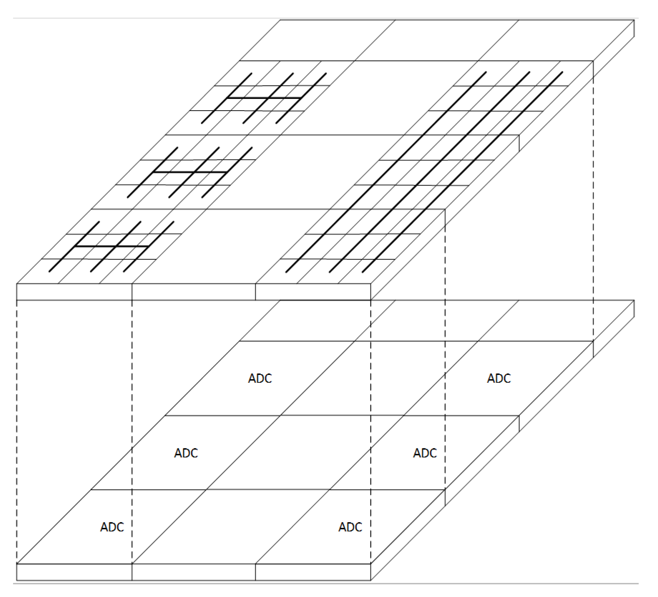
This work is part of a broader research work, whose goal is to design specialized column readout circuitries aimed for sub-electron readout noise performance, as well as fast and low-power imaging devices, being targeted for 3D-stacked implementation. To introduce this topic, the perspective of a stacked CIS design follows the circuit arrangement structure, whose underlying idea is depicted in
Figure 1.
The 3D-stacking integration comprises several silicon tiers, each with different purposes. The most usual configuration in the CIS domain is the presence of two silicon tiers, one for the pixel matrix (called the pixel layer) and another for the readout electronics, usually known as the logic layer.
One can note that the pixel addressing scheme on the top silicon tier can be one of two possible forms. On the one hand, it may be a concentrated addressing form, which requires grouping the nearest pixels for the pixels addressing scheme. On the other hand, it may be a classical pixel addressing form, whose pixels share a small vertical column bus. Note that the latter case is simpler and more effective to design and to work with, yet occupies the same reserved area per ADC block readout on the bottom silicon tier, when compared with the concentrated addressing form.
Furthermore, the staking design technology not only allows one to accommodate Back-Side Illuminated (BSI) pixels, on the one hand, with further enhancements in the sensor optical response in comparison to Front-Side Illuminated (FSI) pixels, such as the increased pixel Fill-Factor (FF), enabling more light to be captured within the same pixel area. On the other hand, it creates an opportunity to further add more exotic functionalities into the sensor, for instance such as per-region exposure time control, resulting in a high Dynamic Range (DR) imager [
5]. These are just a few examples of the possibilities originating from the 3D-stack technology, apart from the already expected improvements concerning the electrical image device performances.
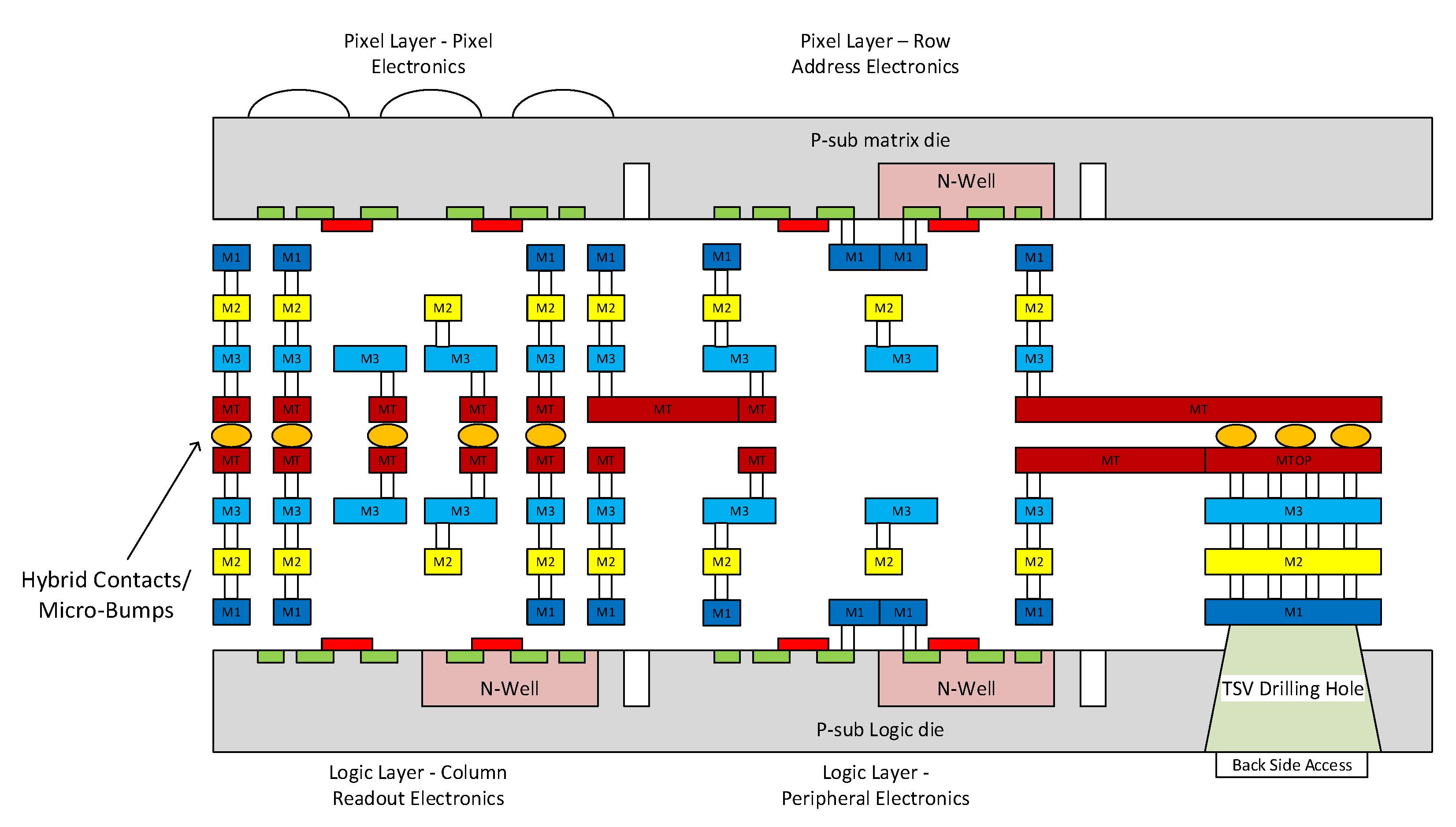
The silicon tiers connection, which in turn performs the readout circuit’s interconnection of the combined 3D-stacked system. In fact, the interconnection is made with Hybrid-bonding (or Hybrid-contacts—HCs), by employing Micro-bump (MB) shapes with contact sizes below 10 µm, which are located in between the Top Metal layers of both tiers [
6]. To obtain a true parallel readout 3D structure, the interconnections must occur under the pixel area, but also spread over the rest of the logic layer. The principle of the tiers interconnection through Hybrid-contacts (Micro-bumps) is shown in
Figure 2.
The top silicon tier drawn in
Figure 2’s scheme is upside down (containing BSI pixels—just for the current example—and usually contains the addressing circuit drivers) relative to the bottom silicon piece (containing all the readout electronics, including the ADCs and all the remaining power electronics as well). The majority of the CIS heat dissipation occurs at the logic layer, and it is preferable for the thermal conduction to occur downwards respective to the logic layer. In other words, towards the external world through a heat sink, or through—the ceramic package, or through another type of thermal sink, as indicated by Remi Bonnard [
7], given that the largest portion of the power consumption is, for obvious reasons, generated in the bottom silicon tier, i.e., the logic layer.
Figure 3 depicts the simplified view of a hypothetical vertical stacked image system, with two optical electronic silicon tiers properly assembled, and shows how the heat conduction should occur, towards the underneath holding heat sink piece.
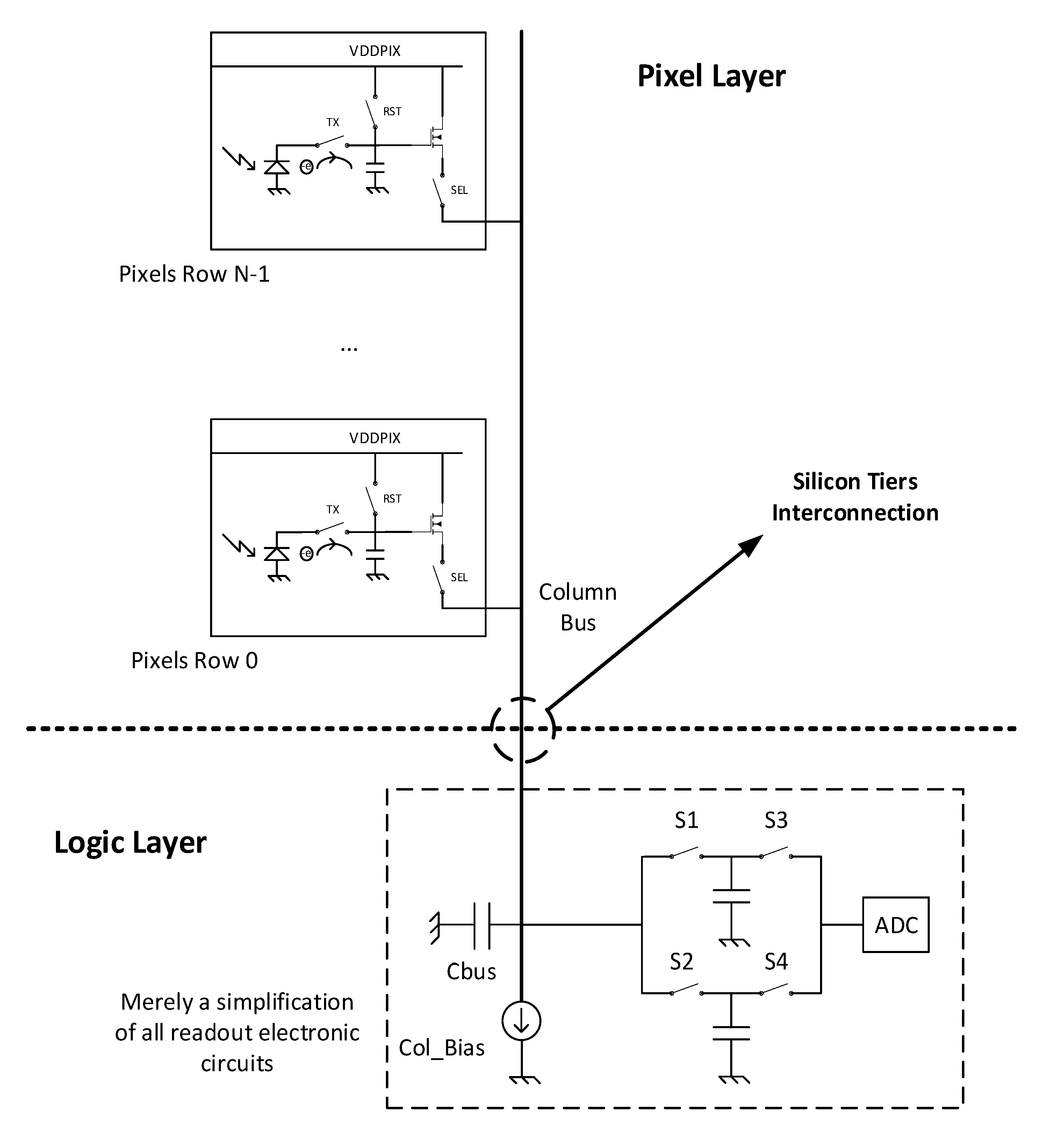
Concisely, and for the sole purpose of exemplification, the different circuits’ interconnection occurs classically in the following form, as shown in
Figure 4. The drawing is merely for illustration, indicating which circuits usually belong to which tier. For instance, the pixel circuits are located in the top silicon tier and the readout circuit chain (which includes any digital circuitry associated with the pixel signals readout, such as ADCs, shift registers and serial drivers, among others) is located in the bottom tier, or in other words, the logic layer.
There are other forms of silicon dies interconnections, such as the Through Silicon Vias (TSVs) [
8], which are usually placed across the chip IO Ring, as suggested by Seiji Takahashi et al. [
9], or at the silicon peripheral area [
6,
10], which is normally reserved for the readout circuits, as well as for the remaining components of the chip surrounding electronics.
Furthermore, it is possible to implement the combination of TSVs and HCs in the same die [
6], but this will not be further explained here, as it falls outside the scope of this research work.
An important issue concerning 3D imaging systems, which is crucial for the reader to bear in mind at this point, is the suitable pixel type to employ on 3D-stacked CIS devices. There is a considerable variety of pixel structures, such as 3T, 4T, 5T and 6T, among others, with up to 8 Transistors per pixel (8T pixel type), including some of their own variants, such as those which are used for Binning schemes, among others.
In FSI sensors, the choice of Rolling-Shutter (RS) or Global-Shutter (GS) pixels depends on the target application, where the motion speed and the image noise may dictate or contribute to which addressing scheme should be employed. The same issue occurs for BSI sensors, namely the definition of the appropriate pixel to choose.
However, in 3D-stacked integrated sensors, the RS addressing becomes critical due to spreading the amount of total pixels over the sub-regions, consequently worsening the usual RS image distortion, as it may create false discontinuities [
11,
12] of the objects from the Filed-of-View (FoV) from adjacent sub-regions, which in turn would be visible in the resulting images.
Depending on the circuits’ arrangement, discontinuities may occur depending on the shutter direction implemented in the stacked sensor for each region of pixels belonging to a particular readout circuitry [
12]. Given these issues, the use of RS pixels in 3D-stacked sensors disturbs and distorts the images much more than in 2D flat sensors, if classically operated. For this reason, the adequate choice for low-noise 3D CIS design is GS pinned-pixels.
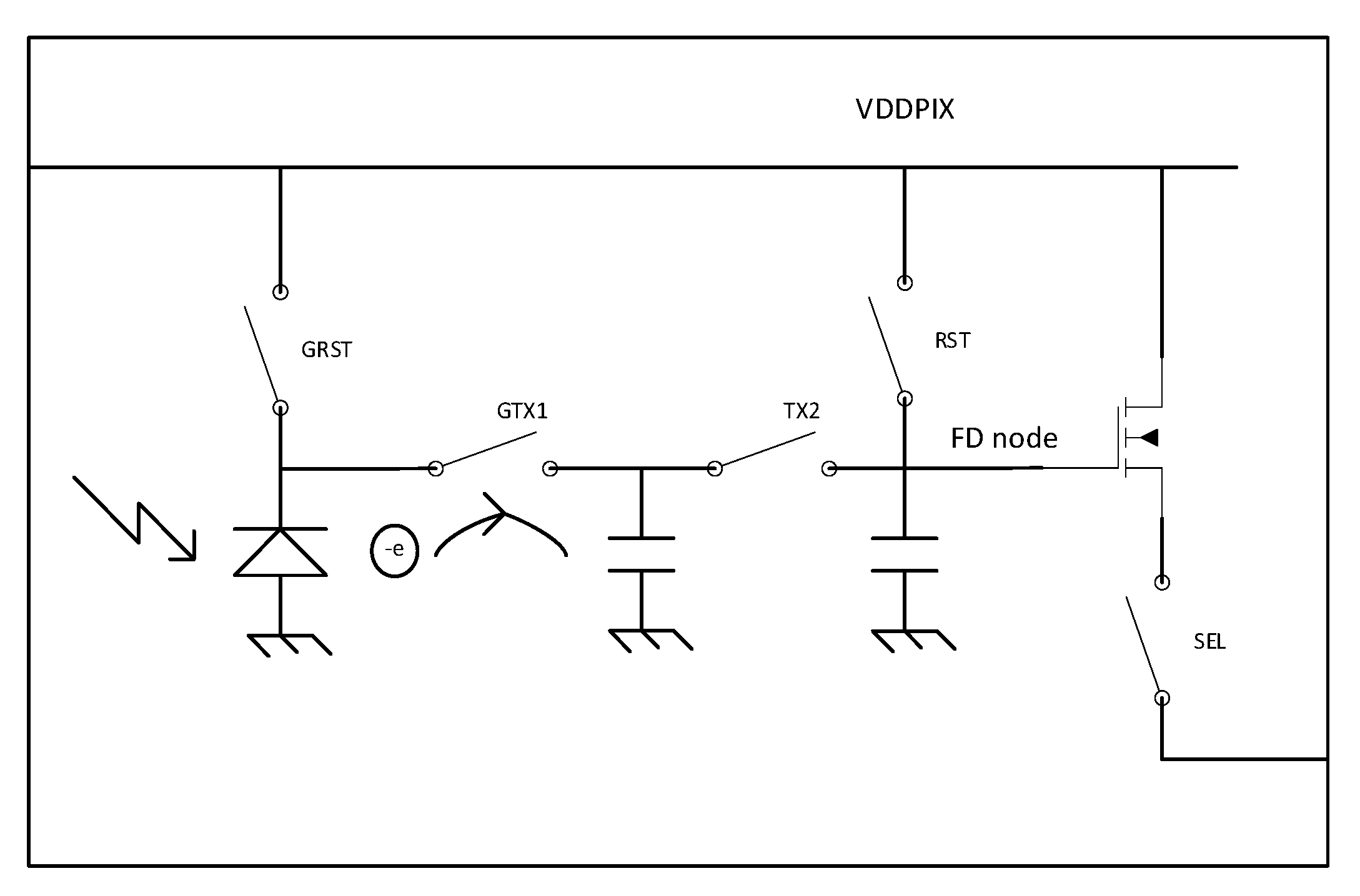
Furthermore, to allow true CDS operation of the vertical stacked sensors, simple 5T GS pixels are far from being the ideal type of pixel to employ, as the light-induced signal is not correlated with the pixel supply voltage left in the Floating Diffusion (FD) node, after resetting the pixel (namely the pixel reset level). This issue leads to the addition of KTC reset noise power into the system, resulting into noisier output images.
From the author’s perspective, the best pixel structure candidate to consider (in future 3D-stacked CIS developments) is the one used by Konstantinos Moutafis [
13], or a more compact GS pixel version, such as the GS 6T pinned-pixel that was indicated by Marius Lunder Lillestol [
14], or the solution that was used by Xiaoliang Ge [
15], which is based on improvements on the classical low-noise 6T pinned-pixel, thus obtaining an improved GS 7T pinned-pixel. The underlying idea of a low-noise 6T GS pixel is shown below in
Figure 5.
The notion that the above GS pixel is related to a low-noise light-to-charge structure has to do with the fact that the resulting photo-signal comes free from KTC reset noise power in the readout chain, as the light-induced signal is well/fully correlated with the reset level signal, previously left in the FD node.
Briefly put, the 3D stacking design does indeed offer a high parallelism of the readout circuits, leading therefore to a reduction of the pixel readout bandwidth, when compared to flat 2D image devices. Moreover, given that the readout circuits are located underneath the pixel array (in stacked sensors), then the parallelism can remain constant at any spatial resolution, enabling both low-noise and high frame rate (FR) levels, at virtually any pixel array resolution.
3. Low-Light, Low-Noise Imaging Background
As this paper is part of a broader research work, it is worth mentioning the legacy work (regarding the low-noise test chip CIS fabrication), employing RS 4T pinned-pixels under a column parallel readout structure. The fabricated CIS had per-column Programmable Gain Amplifiers (PGA) followed by per-column ISD converters, performing both Analogue and Digital Correlated Double Sampling (CDS) operations. The Analogue CDS (ACDS) technique is performed while the PGAs’ offset cancellation phase takes place, and the Digital CDS (DCDS) operation occurs while the ISD ADCs are converting both pixel signals, namely the reset level and the light-induced signals. This combined dual CDS operation enabled the test CIS to obtain low spatial noise/non-uniformity, and also helped to achieve low temporal noise.
It is widely known that the CDS technique produces significant benefits with regards to flicker (1/f) noise cancellation, which is partially removed from the readout circuits due to its high-pass filtering effect [
17,
18]. The ACDS partially removes the 1/f noise power from the PGA stage circuits, while the DCDS removes part of the flicker noise power from the ADCs. The oversampling and the noise shaping effects of the ISD converters are then beneficial features concerning the total thermal noise power contribution to the system, as well as extending to flicker noise reduction [
19,
20,
21], knowing that the oversampling effect intrinsically performs a multiple sampling operation, also known as the Correlated Multiple Sampling (CMS) technique.
Given the introductory information mentioned above, the reader may note that the legacy test CIS fabrication produced a noise floor level below 3 e−rms, with an externally sourced pixel supply voltage, originating less than 0.8% of the entire system Integral Non-Linearity (INL). The legacy CIS also exhibited an exceptional spatial noise level, namely a low Dark Signal Non-Uniformity (DSNU) value of less than 2.6 DNrms@14-bit, due to the dual sampling operation of both the ACDS and the DCDS. Additionally, the legacy test chip pixels presented a Conversion Gain (CG) slightly higher than 105 μV/e− (at unitary system gain), meaning that the total FD parasitic capacitance is slightly smaller than 1.6 fF. The fabricated test chip Saturation capacity was, in turn, roughly higher than 6.4 ke− with a Full Well (FW) capacity of 6900 electrons, being only limited by the ADC input signal range, which was foreseen to be around the 700 mV range, thus being in accordance with the literature concerning 3rd-order single-bit Incremental SD converters implementations. All the above features are experimental from Freitas et al.’s [
2,
4] works.
Adding further information to the above legacy test chip electrical and optical performances, the specific ADCs circuits had consumed (per column) 350 μW of power and the specific PGAs circuits another 135 μW. It then totalized roughly 485 μW of power at 3.3 V analogue supply. This does not take into account, however, the additional 500 μW of power consumption (per column) that is required and reserved for the on-chip power-hungry ADCs references drivers. Since the per-column total power consumption lies in the order of 1 mW, which is a concern for the driven experiment, which is meant for practical and commercial devices, then the solution for the power saving (relative to the ADC references generation) is proposed in Freitas et al. [
3]. The power saving amount lies in the order of 50%, by delegating the references generation to the off-chip. Further details are presented to save more power, whose technique is adopted in this research work and is described upfront.
The downside of the fabricated test chip is that the produced temporal noise was significant, namely for a CIS development that was supposed to be one-step away from a sub-electron solution. In any case, while the test chip was under development, Design-For-Testability (DFT) countermeasures were added [
3], to perform additional tests on the on-chip column circuits. Therefore, important conclusions in terms of the circuits’ adoption for future CIS designs [
4] can be noted, so that sub-electron noise performance can be reached, while maintaining the positive features of the legacy CIS implementation.
Research works aiming for a sub-electron temporal noise specification in the dark always rely on exceptionally high CG values on conventional pixels. This mostly happens because the pixels exhibit tiny FD capacitances, totalizing very small FW values. This leads to a substantial resulting DR degradation, especially when the device is intended for a commercial purpose. In fact, this research work is no different from those works; however, it has the objective of being an early stage of a commercial solution, rather than being a purely experimental and academic work. That being said, the fabricated legacy pixel exhibited a CG above 105 μV/e−, without requiring any fabrication process optimization and/or adopting high-end/complex layout pixels. For the sole purpose of pixel structure demonstration, the fabricated legacy CIS pixel layout is depicted in
Figure 6.
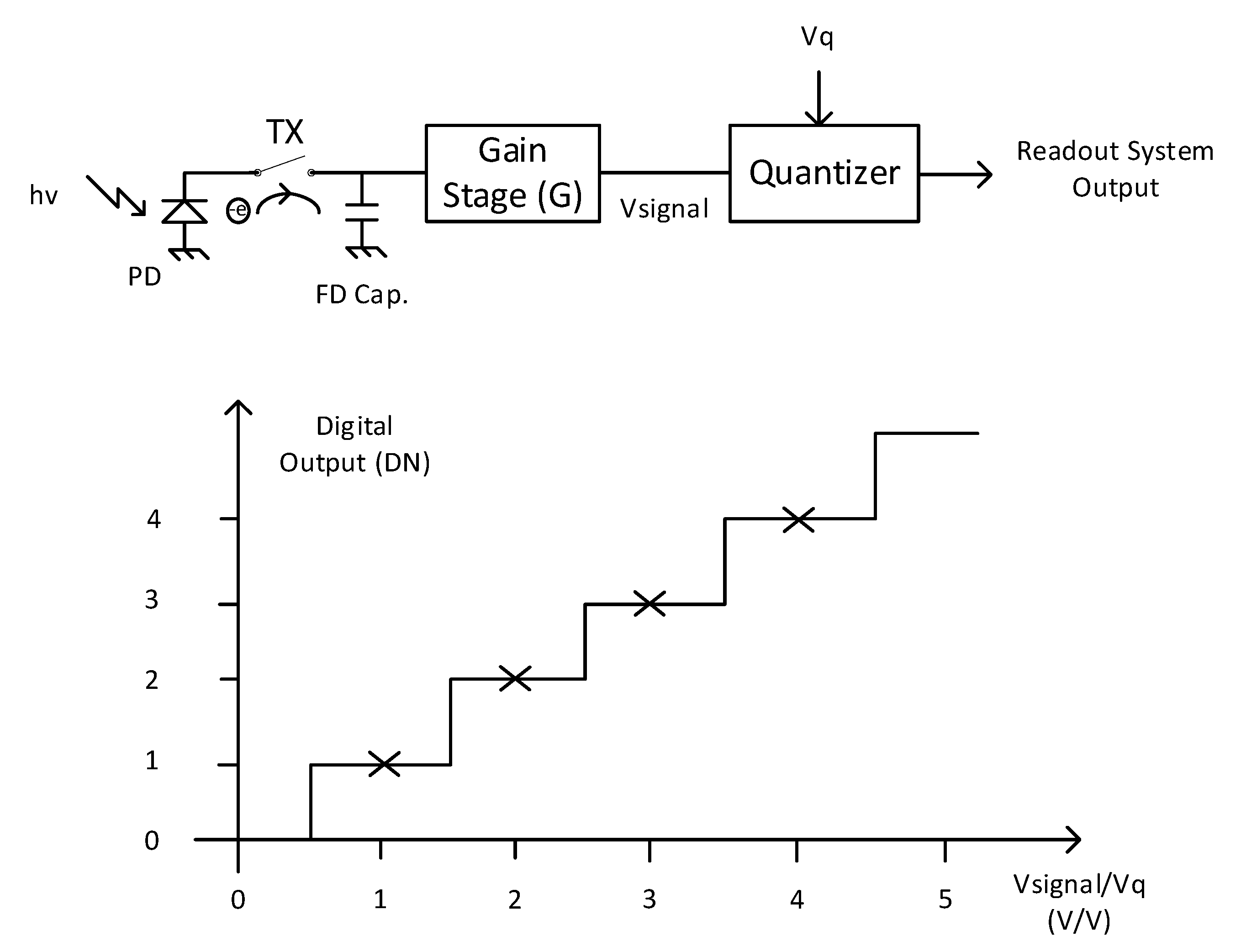
For a clear understanding of how the pixel CG plays an important role (apart from the proper choice of readout circuits and ADC resolution), the problem can be tackled in the following way, as addressed by Seitz et al. [
22], whose underlying idea is shown below, in
Figure 7.
The illustrated system is thought to work in the following way: once a photo-generated electron is transferred to the FD node (with
capacitance tied to the sensitive node), there will be a
voltage step generation, based on the pixel CG value, whose voltage can be further amplified in the system. If
electrons are photo-generated (during the exposure time), then the delivered photo-signal (to the ADC input node) is:
Ideally, the ADC quantization step () should at least match the quantity so that for every photo-generated electron, it can produce a unit LSB (or 1DN) variation in the ADC output code. In the case is set smaller than , then the electrons counting resolution becomes finer, and hence better. In general, the system gain () is set to unitary, except for the cases where the CIS DR is sacrificed in exchange for the overall noise reduction, due to the partial ADC noise contribution to the system. In this sense, and to ideally count photo-generated charges at unitary system gain, the total input-referred RMS noise (expressed in μVrms) must be smaller than , preferably assuming that the .
To conclude the subject, the introduction of gain can be moved further upwards in the readout chain. Instead of being located at the PGA stage, which most of the time is exclusive for this stage, there is also the possibility to obtain extremely High CG (HCG) pixels, not only having extremely low FD capacitance values, but also by enabling in-pixel amplification capabilities, known to be a useful means of reaching extreme noise performance, thus enabling photon-counting capabilities. This may occur not only due to the HCG feature, but also due to the combination of the HCG values, in conjunction with the usage of amplifying PMOS devices, or with the usage of Buried-channel NMOS devices as the pixel SF driver, given the low 1/f noise power offered by these devices [
22,
23,
24,
25,
26]. Nevertheless, none of the previous specific cases will be further discussed in this paper, as they serve only the purpose of proper contextualization.
4. Problem Description
Given the previous background information regarding the 3D-staked technology and its possibilities, in what concerns the increase of CIS performances, such as parallelism, speed and resolution, as well as bearing in mind the low-light imaging requirements and specifications, it is possible to already foresee at this stage, some limitations in reaching sub-electron readout temporal noise performances. This is mainly due to the following reasons:
The readout circuits are too noisy, or they intrinsically exhibit too high a noise value, when compared with the threshold signal detection, when a photon-generated electron is captured and the charge is transferred to the FD node.
The pixel (or the system) lacks a sufficient CG value, so that a photon-generated charge can produce enough voltage signal to overcome the threshold level of the entire readout noise floor.
Or, the conjunction of both issues above, namely the intrinsic readout circuit’s noise (regarding the entire readout signal chain) and the available pixel CG.
In order to be able to obtain competitive commercial imaging CMOS devices, a balance between the two above mentioned features needs to happen to an extent, not only to allow the sensor to detect low-light image variations, but also to enable the sensor to exhibit details (in the output images) at high illumination levels. The latter case occurs when CIS are almost saturated, dictating to a degree a minimum FW capacity for that purpose, whose FW capacity value will depend on the target application.
One can note that improving the CG, the DR, the FR and the Power and Noise performance simultaneously seems impossible to achieve—the best solution must be a good balance between all these features. This is therefore the main goal of the whole research work, which started with a CIS test chip fabrication, to validate the functionality of the newly designed 14-bit high-order, fast and low-noise ISD ADC, apart from validating the most suitable circuits for intermediate readout stages to employ in future designs.
To summarize the problem at hand, foreseeing the next section, the goal is to use the experimental data gathered from the test CIS characterization, such as the pixel CG, among others, to the benefit of a newly enhanced readout circuit. The information about the correctness of the CIS circuits’ operation must also be taken into account, as it involves the design of parallelized high-order 14-bit ISD converters, whose stability is difficult to guarantee, and thereby to ensure its correct functionality across the entire signal range.
In addition, the goal is to use the outcome of a comparison work obtained from the characterization of the several on-chip PGA amplifier circuits [
4], to conclude which type of amplifier circuitry is the most suitable one for further usage in future CIS designs. One should also use this same information regarding the suitable amplifier circuits to improve the noise of the modulator integrators, so that an extreme low-noise ISD converter can emerge and be linked with the rest of the readout circuits.
As soon as the best ADC performance is met (mainly optimized for power and noise), the entire newly adopted readout circuits must be properly tested and evaluated, with the purpose of verifying the overall readout chain noise generation, under realistic supply noise conditions, in a simulation environment.
6. Low-Noise, Low-Power, 14-Bit ISD ADC Performance
The most important block in the readout path is the signal converter, given that it is inside this block that the analogue pixel signals are converted into the digital domain. On top of the importance and the complexity of this block, the stage itself is usually responsible for generating significant noise contribution to the system, and is the reason why there is a dedicated effort in improving the legacy ADC oversampling system, based on the conclusions and the data retrieved from the test chip characterization. In this sense, the goal here is to focus on the enhancement converter performance, regarding both the intrinsic noise and power consumption.
In fact, the enhanced high-order oversampled converter system should preferably have a lower conversion time, while adopting the same design instructions that is stated in Freitas et al.’s [
1] work, in what concerns the converter functionality and the modulator stability. With regards to this last detail, it is necessary to use equal modulator loop coefficients and the use of decreasing feed-forward coefficients. By doing so, the converter input signal range is then capable of reaching a 700 mV level, for a 1 V ADC outer references range.
The noise floor level of the legacy simulated ISD converters (supplied at 3.3 V using thick-oxide devices) was less than 90 μVrms input-referred noise [
1], evidencing low INL value, and with DNL limited from +1 DN to −1 DN, ensuring ADC monotonicity. Therefore, the new and enhanced ADC must exhibit therefore considerably less intrinsic noise compared to the former one, if one wishes to reach a sub-electron CIS readout performance, while maintaining the same design and layout details for its structure. This is crucial to maintain in order to increase the chances of the new converter system behaving without any unexpected artifacts associated with its operation, when going to its physical implementation in the future.
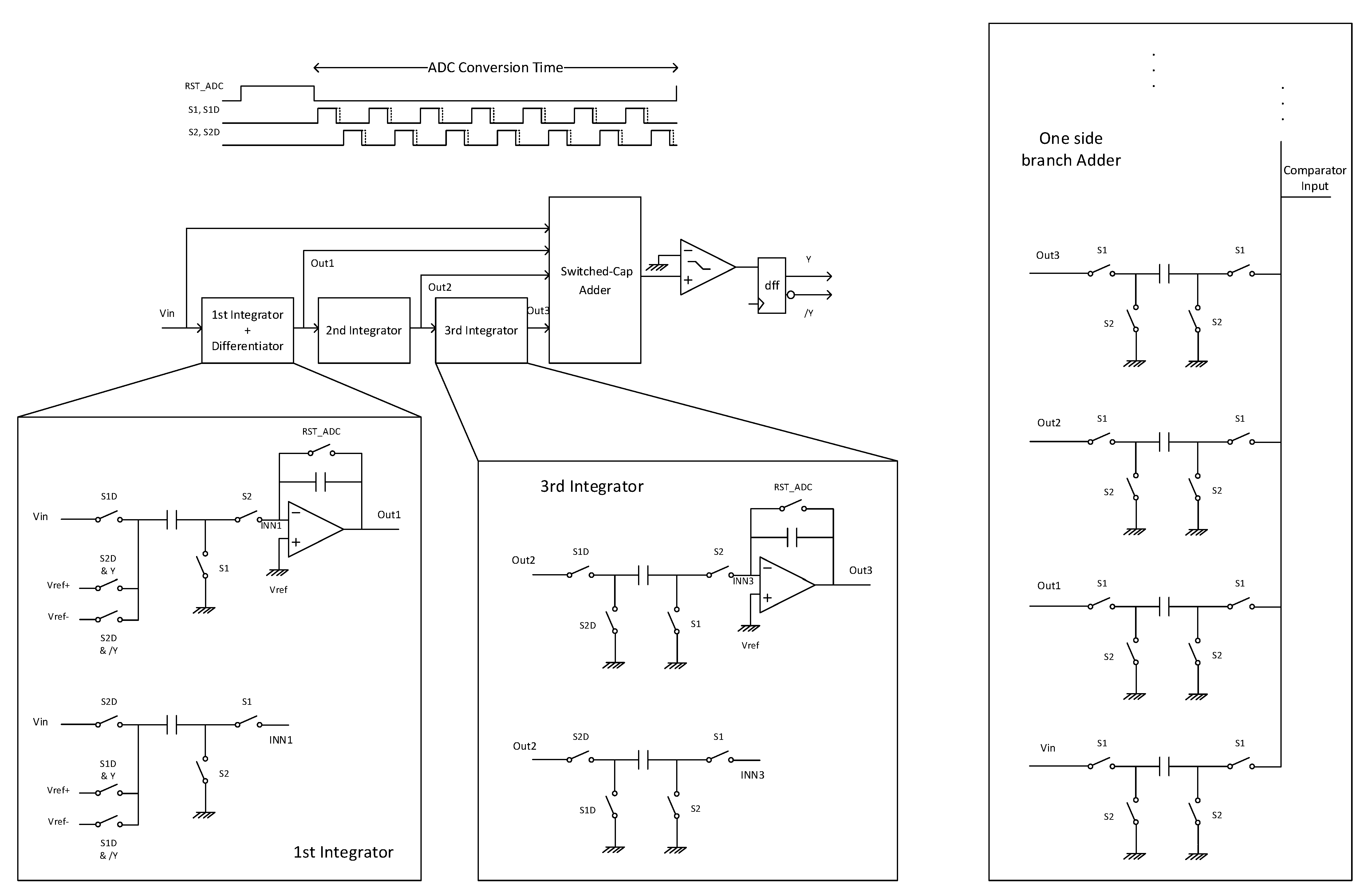
Figure 8 and
Figure 9 depicts the block level structure and the detailed transistor level design of the enhanced oversampling ADC system, which is targeted for noise performance and lower voltage supply, due to power dissipation issues.
Further understanding of the block operation, the specific dual clock phase operation and its operation theory, concerning the ADC functionality, can be found in Freitas et al. [
1,
2,
3], as well as in Markus et al. [
27,
28,
29] with regards to the generic system converter operation. The converter references range is by default meant to be for 1 V span, where only 70% (approximately) of the references range is indeed useful for the input signal, to maintain the modulator circuit stable, for the 3rd order single-bit ISD converters.
The enhanced low voltage supply 14-bit converter is capable of detecting input variations of 61 μV steps. In fact, this is exactly the quantization step of an ISD converter under the influence of 1 V span outer references. The maximum output code that can be generated is somewhere around the 12,500 DN code, due to the inherent loss of the converter dynamic range required to maintain the modulator stable in 3rd order ISD converters.
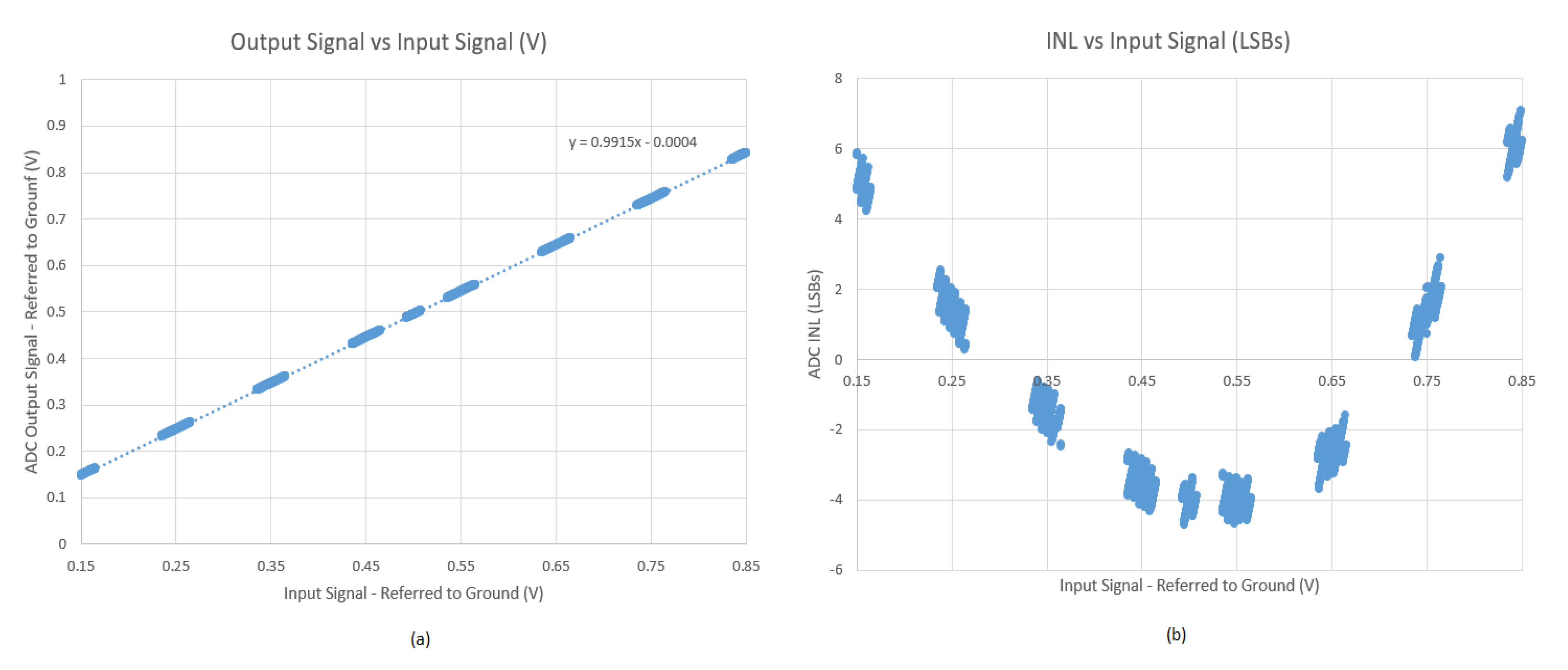
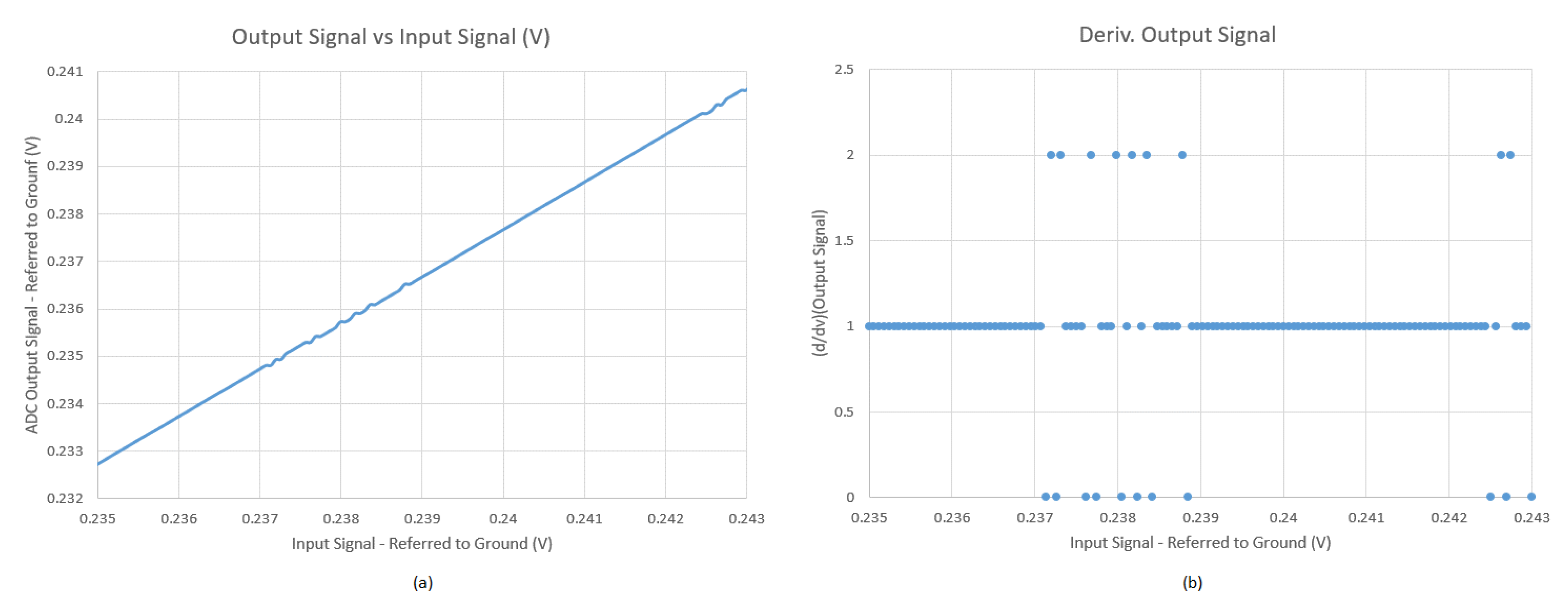
That being said, for every 61 μV variation driven at the converter input node, there must ideally occur a 1DN output variation. This issue is addressed with
Figure 10a information input-to-output response. The extensive parametric simulations (almost 3000 tests) were based on 61 μV input signal steps, across 700 mV input range, in a distributed manner. The resulting characteristics of the enhanced converter, which outputs linear data with a gain factor of 0.9915, indicate, from a first perspective, a fairly correct conversion operation, given the almost unitary value relation between the input and the output.
Furthermore, the converter INL is shown in
Figure 10b, as part of the enhanced system verification. The absolute INL data provides evidence that the converter exhibits a non-linearity of 6 DN, namely a half-way value from −5 DN to +7 DN, concerning the lowest and highest points. This is an exceptional INL value for such a complex 14-bit converter system.
Concisely, the simulated 6 DN INL lies in the order of a 0.05% signal range, which is by far an irrelevant effect on the entire system non-linearity, whose value is usually limited to 1% of the signal range, mostly dictated by the non-linearity of the pixel SF. Therefore, one can conclude that the improved ADC, based on thin-oxide low voltage devices and based on CS Cascaded integrators amplifiers, has reached input-to-output signal performance similar to the legacy converter [
1,
2,
3,
4], while not showing any signs of degradation, which is imperative.
Summarizing the
Figure 10’s input-output characteristics, the converter exhibits true 14-bit precision with an intrinsic INL of 6 DN, operated at equivalent 20 MHz clock frequency, producing 14-bit words, roughly at every 6 μs. The modulator stability is guaranteed through 0.36 values (
) concerning the modulator coefficients, where the feed-forward coefficients are ruled by the following relation:
, namely 2 > 1 > 0.5, respectively.
The legacy test chip modulator design required approximately 32 μA per integrator stage (in average), plus 15 μA reserved for the comparator, totaling roughly 110 μA current consumption at 3.3 V, while for the current improved version of the same modulator, the average current consumption dropped down to 27 μA per integrator stage, totalizing roughly 96 μA of the modulator current consumption supplied at 2 V, in order to fully explore the ADC dynamic range.
By adopting single-input CS Cascaded amplifiers (used in this work) rather than the differential-input Push-Pull amplification structures (used in the legacy work), this has led to approximately a 13% current reduction, which is already significant, concerning the power dissipation through a higher current usage efficiency.
One should note that although the speed is important, it is not as crucial as the power consumption. Therefore, the enhanced ADC design power was preferred over speed, given that the achieved 5.9 µs conversion rate was already a reasonable value for 14-bit converter precision. Nonetheless, the conversion system can operate at higher speeds, by simply increasing the clock frequency up to 1.5 times higher, since the modulator circuits have enough margin to operate that much faster, but at the expense of degrading some of the converter features, such as the ADC input-output characteristics—hence the converter linearity, as shown in
Figure 10a,b.
Figure 11a presents a zoom-in figure of the converter characteristics, and
Figure 11b depicts the corresponding derivative converter response, shown for a short signal range, for DNL assessment purposes. It is worth mentioning that across all input signal ranges (from 0.15 V up to 0.85 V within the ADC references) the noise-shaping converter had produced the majority of the output derivatives, as unitary values. In fact, only a small percentage of all points (within the ADC range) exhibited derivatives either equaling null or two. This is perceptible in the zoom-in figure of the short-range derivative values, namely in
Figure 11b, where the majority of the points are unitary. In this sense, this is what makes the input-to-output ADC characteristic response quite close to unitary, as depicted in
Figure 10a. Therefore, one can conclude that the enhanced low voltage incremental converter continues to be a monotonous system, and no missing codes were observed.
Thus far, the enhanced thin-oxide design ADC input-to-output response characteristics, namely the INL and the DNL, have been addressed above, which presents similar ADC INL and DNL features compared with the legacy work [
1]. The features must remain this way, as the most relevant pay-off effect comes with the next performance feature, namely the intrinsic converter noise performance. That being said,
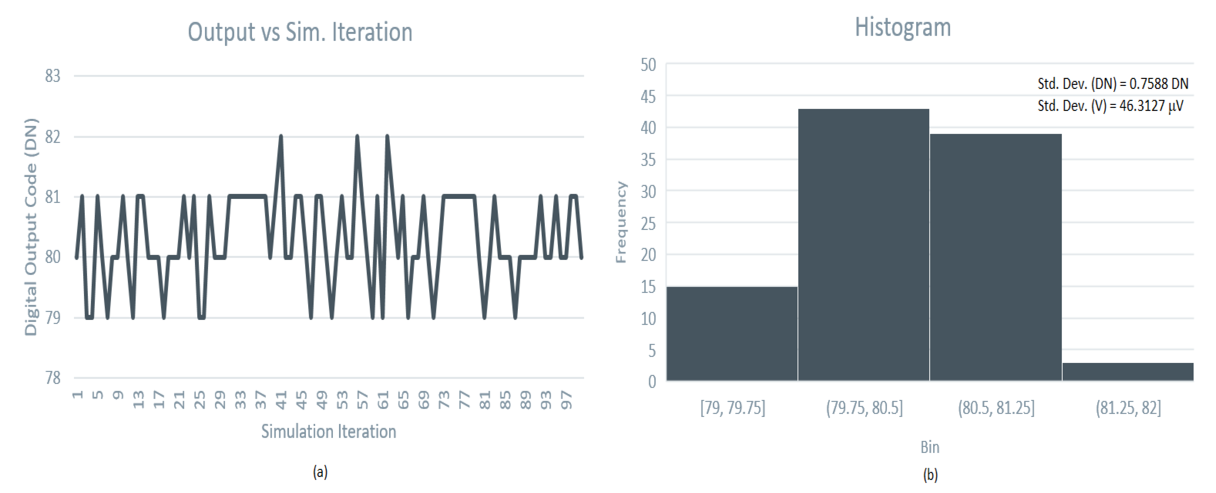
Figure 12a depicts the converter output codes and
Figure 12b depicts the noise results (hence the resulting output codes dispersion) of an extensive and time-consuming Transient-Noise simulation, under a DCDS operation, with a static DC input signal, equivalent to low-light input signal scenario and with the ADC subjected to 5 mVrms noise on the power supply node, plus an additional uncorrelated 5 mVrms noise applied on the ground. It is necessary to subject the modulator circuits operation to a more realistic on-chip power supply environment, such as in this case, rather than using the traditional clean power supplies tests, which is not a realistic case in the slightest.
The extensive and time-consuming 100-run Transient-Noise noise simulation produced four possible output states, around a medium output value. The number of occurrences near the mean output ADC value is much higher than the remaining ones, thus indicating a larger concentration of those, which becomes more perceptible when these occurrences are plotted in a histogram graph.
The Root-Mean Square (RMS) of the output values distribution is roughly 46 μVrms, in opposition to the 89 μVrms noise (under clean supplies) exhibited from the legacy ADC design in [
1]. Since the 14-bit ISD quantization step (
) equals 61 μV, based on the 1V-ADC references range, spread over 16,384 ideal codes, then one can conclude that the intrinsic converter noise (under a 5 mVrms power supplies noise—both VDD and GND) is smaller than the ADC resolution, and evidences a robust noise-shaping converter, especially in terms of intrinsic noise performance.
As long as
(for a unitary system gain), and the sensor CG is higher than the simulated intrinsic noise, then the photo-generated electron detection is guaranteed. However, one still needs to take into account the complete readout circuit’s noise, to verify how far or near the system is to the electron-RMS noise detection. This will be the subject of discussion in
Section 7.
Lastly, but equally important,
Table 1 summarizes the performance’s key features of the simulated low voltage enhanced third order ISD noise-shaping single-bit converter.
One can note that at an equivalent 30 MHz clock frequency (i.e., at 1.5 times 20 MHz), the conversion rate would drop down to less than 3.9 μs for every 14-bit word generation.
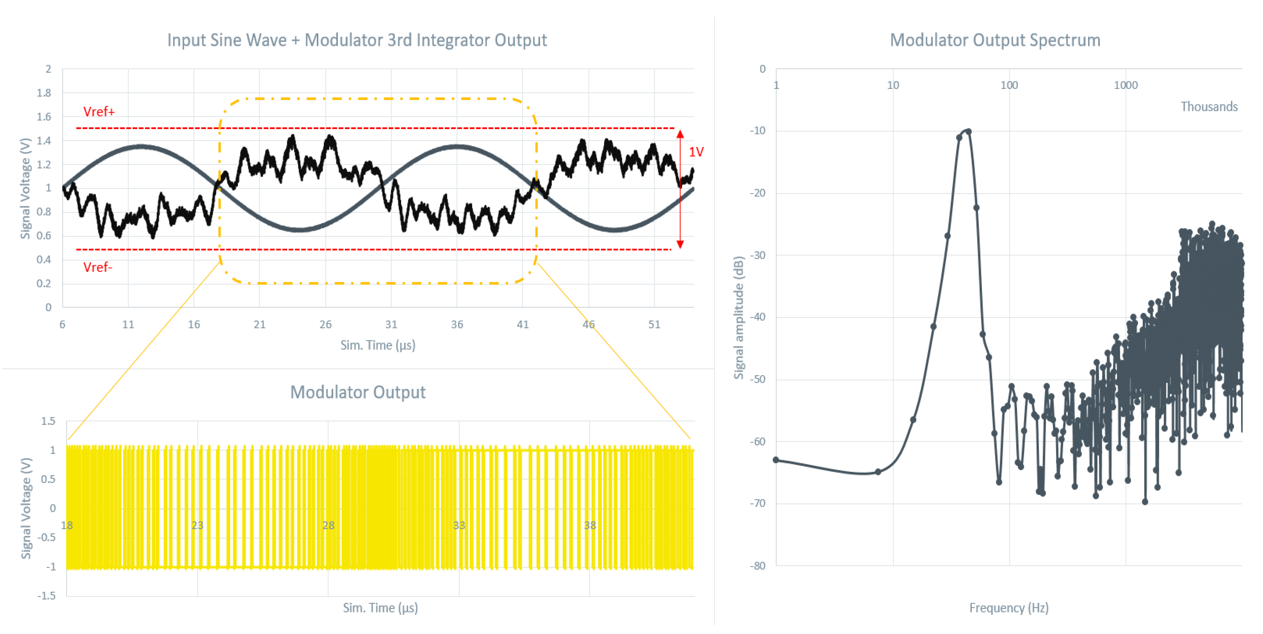
The reused converter is an Incremental signal converter, meaning that the oversampling system averages the input signal, but behaves similar to a single-shot ADC—in other words, similar to a Nyquist-rate ADC system. Hence, just for the clarity of the system, and while the modulator is operated in a free-running mode,
Figure 13 shows some of the relevant signals for this specific modulator free-running mode operation.
The input sine-wave signal (for the free-running modulator test) has a peak-to-peak value of 700 mV within the 1 V converter references range, being such a requirement for the stability of the 3rd order modulator in conjunction with the appropriate modulator coefficients. Furthermore, the output node signal of the last (3rd) integrator within the converter modulator is shown as well, as it is the most important signal to verify the system stability, therefore being once again a requirement for the system to be able to perform correctly. As long as the last integrator output node signal stays bounded to the references signal, then not only the modulator is stable, but the quantization step can also be predicted while staying below a limit, thus defining properly the converter resolution. In addition, the modulator output bit stream is shortly displayed, corresponding to a full period of the input sine-wave signal, and also displays its corresponding spectrum as an output of the Spectre simulator Fourier transform, based on using a Hanning window with 8192 points.
7. Complete Low-Noise, Low-Power Readout Circuit Performance
To take into account the noise addition from upward stages in the readout chain, and to unveil the noise performance of the entire enhanced low voltage supply readout system, which is based on thin-oxide low voltage transistors and on suitable CS Cascaded amplifiers, an additional Transient-Noise test (including all the readout electronics) was performed. This included a 4T pinned-pixel model (based on the test chip design and extracted from the fabricated device optical/electrical characterization), in addition to the re-designed enhanced signal conditioning readout circuits, namely the AC-coupled low voltage PGA stage, plus the low voltage noise-shaping ISD ADC stage. Although the GS 6T pinned-pixels are the suitable pixels for future 3D-stacking designs from the author’s point of view, to avoid chopped output images [
12], the legacy RS 4T pinned-pixel accurate model was used (included in the simulations), for the sole purpose of verifying the enhanced readout circuits’ performance.
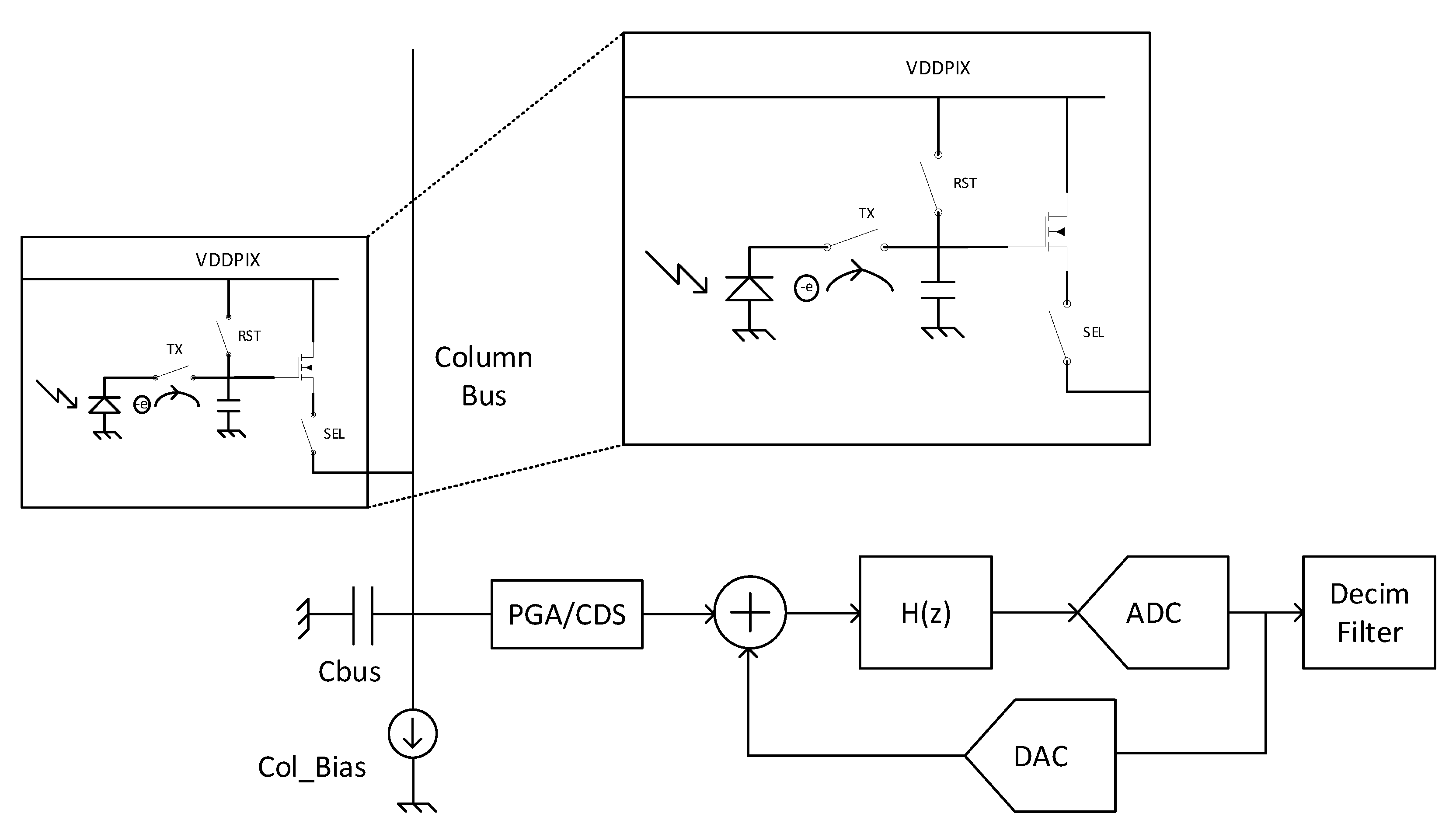
Figure 14 depicts the simplified readout block diagram used in this research work, showing the presence of the column PGA and the column ISD converter, whose built-in amplifiers are CS amplifiers. In addition to this,
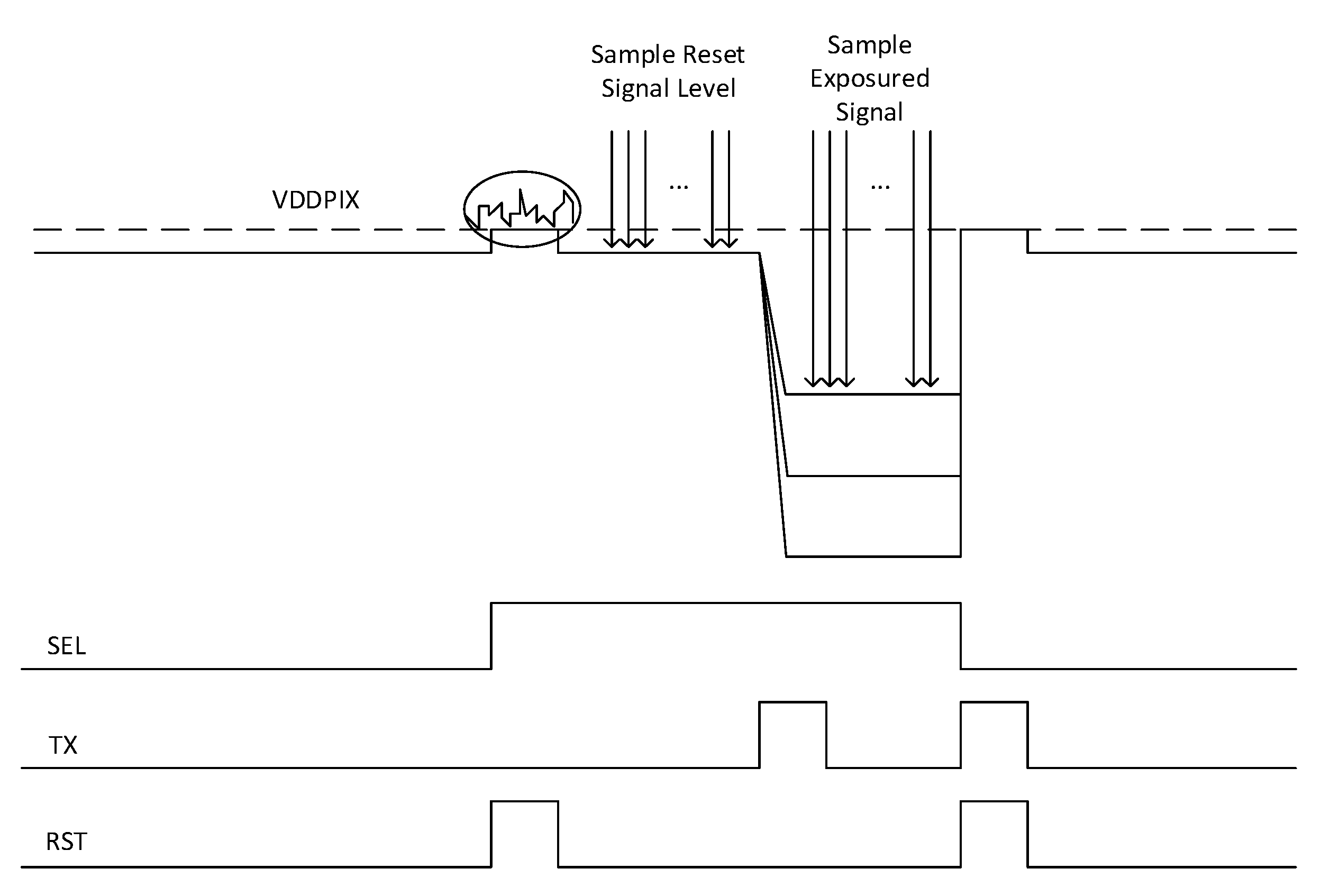
Figure 15 displays the pixel timing operation and the simplified analogue version of the pixel signals at the sensitive FD node (namely the pixel SF gate), relative to this RS 4T pinned-pixel.
First, the system reads and oversamples the pixel supply/reset level (left in the FD node after the reset switch operation) in the first AD conversion of the DCDS system operation. Next, the Transfer (TX) Gate is triggered to emulate the transfer of all the collected charges (captured during the sensor exposure time), thus creating the light-induced signal charges, which will be moved to the FD node. After the charges transfer period, the generated signal is read out and oversampled, while the second AD conversion of the DCDS takes place.
The difference between the reset level and the light-induced signal level is the photo-signal. Hence, this photo-signal will appear at the system output (in the digital domain) as a direct product of the DCDS operation. Note that the system not only outputs the photo-signal, but also outputs the random temporal noise present in the readout. Furthermore, one can note that any given spatial noise that may exist in a real system employing these circuits will be strongly attenuated, given the overall double sampling effect, both in the analogue domain, as well as in the digital form, as occurred in the legacy test chip and reported by Freitas et al. [
2,
4].
The pixel devices are: the RST switch W/L = 0.42 μm/0.42 μm; the SF driver ratio W/L = 0.6 μm/0.8 μm; the SEL switch ratio W/L = 0.6 μm/0.42 μm; and the TX (Transfer) gate, which has an experimental parasitic effect equivalent to a minimal device area, namely with the physical size of W/L = 0.22 μm/0.35 μm.
The important part to retain from the suggested CS Cascaded PGA amplifier circuit pointed by Freitas et al. [
4] is that the reference level for the first conversion of the DCDS (namely the FD node signal version of the pixel reset level at the ADC input node) can be properly set and defined, based on the PGA reference. Therefore, the corresponding sensor optical dark signal can be driven at an appropriate position within the ADC signal range, to allow the matching and maximizing of the pixel signal within the ADC dynamic range. For instance, if the ADC has its outer references signals generated at 0.5 V and 1.5 V, respectively (Vref− and Vref+), with the virtual ground reference (Vref) at 1 V absolute voltage, then one must conclude that an appropriate PGA reference could be 0.65 V, already taking into account the expected 700 mV input range, equally split and centered at the ADC virtual ground. This is the major positive effect of having PGAs when compared to the simple column SF stages as active elements, to drive ISD converters [
4].
Given the above introduction of the re-designed (thin-oxide) low voltage enhanced readout circuits, which are employed in the current test for noise performance measurements, the combined
Figure 16a,b shows the noise performance of the entire readout chain. It includes the modeled pixels, the PGAs and the ISD ADCs, as depicted in
Figure 14. The amplification stage performs Analogue CDS while the PGA stage removes its own offset, and the ADCs perform the Digital CDS operation through two consecutive AD conversions.
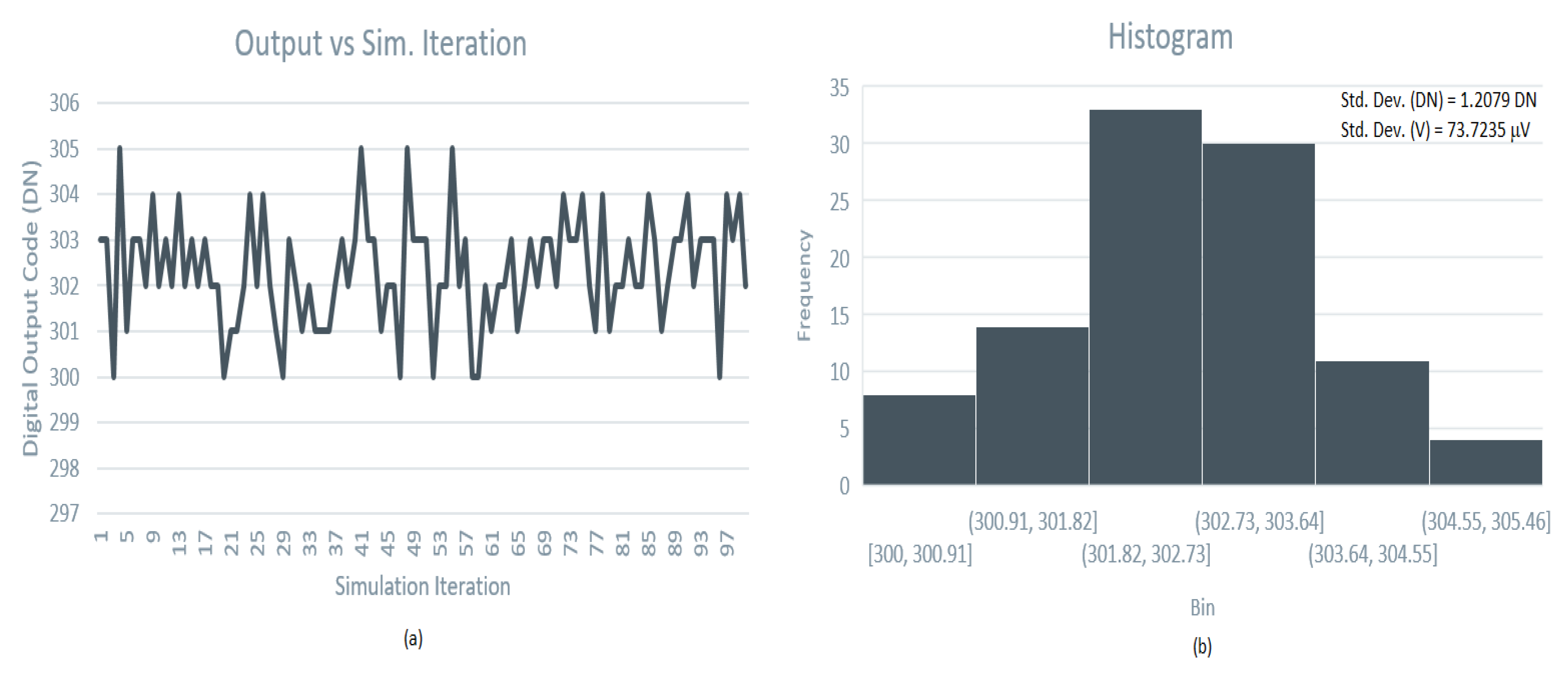
Once again, the extensive time-consuming 100-run Transient-Noise noise simulation, with outputs shown in
Figure 16a, produced values with six possible outcomes (around a medium point) due to the temporal noise present in the system, which was itself due to the intrinsic circuits noise generation and based on the environmental power supply noise present in the system. In the simulation test (which is based on
Figure 14 circuit and operated under
Figure 15 oversampling method), the entire readout circuits were flooded with uncorrelated 5 mVrms noise power, and ground noise as well. This happened similarly for the ADC simulations, whose performance is addressed in
Section 6. Additionally, another uncorrelated 5 mVrms noise source was introduced, namely into the pixel supply, for a more realistic system operation scenario of the sensitive circuits.
By doing so, the outcome of the noise simulations can be seen as something that would very likely occur in a real scenario with a real chip fabrication. This can be inferred based on the adopted enhancements, namely the use of thin-oxide transistors, a low-voltage supply and the use of specific amplifier circuits, as well as being based on the knowledge obtained from the legacy test CIS, which already employs high-order incremental converters.
As a product of the 100-run Transient-Noise simulations performed under a heavy environmental supply noise case scenario, the entire readout chain exhibited less than 1.21 DNrms noise (<74 μVrms) as a result of the Digital CDS operation. This noise value already takes into account the intrinsic noise generation of the entire low voltage thin-oxide circuitries readout path, as well as the addition of the effect of two times the ADC quantization noise. This in turn leads one to the conclusion that the low voltage supply (for power reasons), the use of thin-oxide devices (for noise improvement due to the low 1/f noise power) and the employment of a proper amplifier structure for both the PGA and the ADC modulator were enough to produce less than 1e− input-referred noise, with the current pixel CG of 105 μV/e−.
The previous happened under DC references, and the conclusion of the sub-electron result is based on the extracted CG of the fabricated CIS, whose pixel model was employed in the test benches of the enhanced readout circuits. With such a simulated input-referred noise DCDS value, one can note that the noise floor is then close to 0.7 e−rms. In fact, the resulting simulated noise performance already indicates that the proposed solutions (with the current readout method based on high-order ISD converters) can compete with most of the low-noise modern developments, and is capable of sub-electron noise detection [
9,
23,
24,
25,
26,
30,
31,
32,
33] without excessively degrading the target CIS DR (maintaining it instead), by using classical low-Vth Surface-channel SF NMOS pixel devices.
Bearing this in mind, the method used in this research work, which is supported on the lessons learned and on the experimental data from the legacy test CIS characterization, reinforces the fact that several of the proposed solutions—namely the low noise amplifier structures, the low noise devices, and the low voltage supply—are indeed a means of reaching the sub-electron noise performance.
It is worth mentioning that there is no need to strictly employ a high-end pixel design utilizing process optimization, or the need for PMOS pixel SF devices, or like-wise the need for Buried-channel pixel SF transistors, or even the need for in-pixel amplification, to reach below 1e− RMS input-referred noise. However, this does not signify that to reduce the noise even further to extreme levels (towards photon counting capabilities) the above-cited practices are not critical or necessary to be employed. Nevertheless, for sub-electron detection it is sufficient to use Surface-channel pixel SF devices with an optimized low voltage PGA amplifier and low voltage ADC circuits, performing a high average count CMS technique.
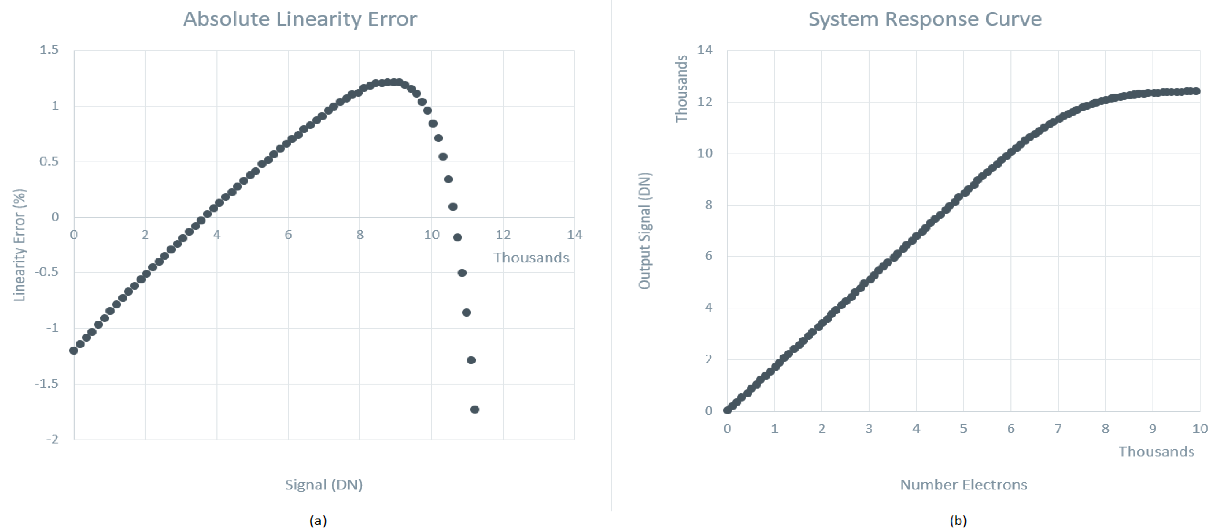
To further characterize the entire readout path (in terms of system linearity), based on the specific pixel model, emulated and included in the simulation environment, the equivalent Photo-Response Curve (PRC), which is based on the EMVA-1288 guidelines [
34], is presented in
Figure 17b with the corresponding non-linearity displayed in
Figure 17a. In this manner, the majority of the readout system non-linearity (coming from the pixel SF driver) will be present and visible for evaluation (
Figure 17a), given that the addition of the converter INL is expected to be insignificant when compared to the pixel SF non-linearity.
Note that the emulated charge transfer effect occurring from the equivalent Photo-Diode (PD) node to the sensitive node is created by an ideal current pulse, whose current amplitude generates a downward FD signal (
Figure 15), corresponding to the photo-signal produced in a real scenario by the RS 4T-pinned pixel, which is then used to test the entire readout path. The equivalent amount of photo-generated charges is related to the current pulse amplitude and pulse width.
From the combined
Figure 17’s parametric simulation results, one can note that the output signal response is fairly linear, in the signal range limited to 6500 electrons (in other words, approximately limited to 11,000 DN code), which is in accordance with the experimental results from Freitas et al. [
2,
3,
4]. This in turn signifies that not only is the employed emulated pixel model correct, but also that the entire low voltage, the thin-oxide devices and the enhanced readout circuit chain do not add much more non-linearity than that obtained in previous research works, i.e., the current system INL stays bounded to 1.2%.
To finalize the subject of the system response behavior,
Figure 17b additionally shows that the output response saturation occurs roughly at 12,500 DN code of the equivalent signal, which is similar to the findings in the previous research works from the same authors, including the clamping effect on the pixel column bus, while maintaining enough signal room for the readout (PGAs, ADCs) circuits to operate. Of equal importance,
Table 2 summarizes the key electrical performance features of the entire low voltage readout path, performing both analogue and digital CDS operations.
It is worth noting that higher DR values are likely to be obtained under smaller system gains, for instance at 0.5 gain, rather than the default unitary gain case, and therefore likely to originate 13 ke− of Saturation capacity [
3], given that the node that limits the signal range is the ADC input node, which is restricted to ~700 mV. Since the fabricated pixel (designed with thick-oxide and supplied at 2.5 V) exhibits much more signal swing (at the FD node) than the 700 mV reserved for the ADC input range [
3], one must then conclude that the resulting DR would increase substantially.
Finally, yet crucially, to compare the improved re-designed readout circuits with others silicon proven in the field of sub-electron detection works,
Table 3 highlights the sensor’s overall performances, in order to have a term of comparison.
To contextualize the reader for an upcoming comparison work, the following must be addressed. A Jot is the designation of a pixel (whether conventional or not, such as Single-Photon Avalanche Diodes—SPADs, which are suitable for photon timing applications [
31]) that has capabilities of detecting by itself photo-generated electrons, and being characterized by having an equivalent extremely high conversion gain, and is hence characterized by HCG values. Furthermore, the Quanta Image Sensor (QIS) is a specific image sensor device capable of sensing impinging photons with time-resolved capability (through 1-bit detection precision) or with photon-counting capabilities (through M-bit detection precision), despite being characterized by having a very small equivalent FW, which is the reason why they are meant exclusively for extreme low-light applications.
Several details should be highlighted before hand, concerning the several competitor works’ performance, from
Table 3. Regarding J. Ma et al. [
31], the sensor is a QIS device, that is characterized by extremely low FW capacitance at the expense of enabling HCG values, to overcome the circuit’s noise floor, so that photo-generated electrons are detected precisely at a point where even the photon could be counted. Since the goal of this research work (jointly with those of the legacy ones) is to unveil a means of developing a low-noise and a high DR CIS with a conventional pinned-pixel structure, then the upcoming performance comparison serves to indicate that if this work had invested in a higher CG pixel, then the re-designed readout circuits’ noise performance (expressed in noise electrons) would be improved by the same factor as the CG enhancement.
For instance, by increasing the current 105 μV/e− CG value of this work to the levels of J. Ma et al.’s [
31] CG value, namely to 242 μV/e−, it would reduce the temporal readout noise in the dark by a factor of 2.3 times, hence resulting in 0.3 e−rms. This means that one could compromise this research work’s inferred DR (with the chosen PGA+ISD column readout structures, performing CMS, with the current modifications and improvements), in exchange for a readout method that would be capable of a photon-counting feature, in the hypothetical case of a HCG pixel. This is relatively easy to verify, as this research work’s noise (expressed in μVrms) is found to be below the 100 μVrms noise. This in turn makes the developed readout circuits capable/suitable of being employed in a hypothetical multi-bit QIS for the CIS readout path, therefore evidencing its own qualities.
A similar case occurs with the M-W. Seo et al. [
30] device readout, when compared to this research work. The M-W. Seo et al. [
30] image sensor exhibited 220 μV/e− CG, meaning that an equivalent case to this work would produce a temporal noise floor level of 2.1 times smaller than the current value, thus obtaining 0.33 e−rms noise in the dark. This noise performance (at an equivalent CG) ends up slightly larger than the device [
30] noise performance. However, it should be noted that the imager [
30] was developed under a 110 nm process node. The 110 nm fabrication process possesses less noisy devices than the 180 nm process transistors, due to higher oxide capacitance and a smaller flicker noise factor, much like what happens with thick-oxide devices and thin-oxide devices in a same foundry process node. In this sense, even in such a case, this work would produce a higher DR than M-W. Seo et al.’s [
30] device at an equivalent pixel CG. Therefore, in overall terms, the re-designed, enhanced, low-voltage supply readout with thin-oxide transistors appears to be more competitive.
Finally, one can note that Boukhayma et al.’s [
26] sensor employs a readout type that is the most similar to this research work’s readout method, from among the selected ones. The Boukhayma et al. [
26] sensor was fabricated with a 180 nm process and operated under a CMS technique, with a CG in the same order of magnitude as the one used in this work, although its pixel CG is substantially higher than that of this work. Moreover, Boukhayma et al. [
26] employed PMOS-based SF pixels, which are also known to reduce substantially the 1/f noise from the pixel/early stage. On the other hand, it was decided that this research work keep an NMOS SF driving device within the pixel, as part of maintaining the pixel in its classical form and keeping the layout simple, without mixing device types within the pixel area.
By judging the ratio of CG values, one can conclude that the noise floor for this research work would be reduced by a factor of 1.52 times (0.46 e−rms) if the pixel had the same CG as the one used by Boukhayma et al. [
26]. However, and as mentioned earlier, one needs to take into account the fact that PMOS-based SF pixels introduces considerably less noise at an early stage in the readout path, which plays a significant role in the resulting noise performance. Nevertheless, and in overall terms, this comparison work reveals that this work’s readout method remains competitive. In this sense, further enhancements can be done directly in the pixel stage if further noise reduction is the target.
With regards to the possible case of further pixel enhancement (if this becomes necessary to perform), the authors view the Buried-channel based SF pixels as a much better choice than PMOS-based SF pixels, since the former, similar to PMOS devices, share a significant 1/f noise power reduction when compared to Surface-channel-based SF pixels, and are the same type of the neighbor transistors. Furthermore, buried devices inherently increase the column bus signal, in opposition to PMOS devices, which thus is the reason why these Buried devices are preferable over PMOS devices.
8. Conclusions
In this work, a 3rd order Incremental SD single-bit converter, which is designed and targeted for column parallel structured 3D-stacked low noise, low power CIS, is presented along with indications of optimized specific column amplification circuit stages, enabling an overall sub-electron detection readout in the dark. The most suitable converter, while performing a CMS technique for low noise performance and reasonably fast conversions (with low 1/f noise power) for vertical stack designs, is the 3rd-order ISD converters, achieving the best balance among the area, power, speed and noise, when compared to other converter orders [
1].
The enhanced ISD converter, which is designed with low voltage devices (for further smaller flicker noise power contribution), exhibited a non-linearity of 6DN, representing 0.05% of the signal range, while staying well below the ~1% non-linearity of CIS classical limits. In addition to this, the converter has revealed to behave and work as its predecessor (the legacy test chip), demonstrating not only good electrical performances, but also correct functionality across the expected ~700 mV signal range (namely ~70% of the ADC references), under stabilized modulator operation, employing specific modulator coefficients as defined by Freitas et al. [
1], such as
and
, namely 2 > 1 > 0.5, respectively.
To further verify the full signal readout path, regarding both the electrical and the noise performances, extensive simulation work was conducted, under the use of a realistic pixel model and the use of a realistic power supply noise contamination scenario, concerning the ever-present on-chip environmental noise. In this research work, three uncorrelated 5 mVrms noise sources were added into the simulations not only for the analogue supply and the ground node, but also for the pixel supply. From these tests, one could conclude that the overall non-linearity obtained is slightly higher than that of the legacy test chip (which this research work is based on), namely exhibiting a 1.2% system INL feature in the linear range of the equivalent light response. This value is within the range of a practical and a commercially viable CIS product INL.
Additionally, the expected saturation capacity of the enhanced low voltage supply (thin-oxide devices), with low power readout (which includes an accurate pixel model), is roughly 6500 electrons; however, it is very likely to be capable of a 13 ke− FW capacity [
3]. Furthermore, the input-referred noise floor level of the enhanced readout path falls below one electron RMS noise, namely 0.7 e−rms, approximately. Therefore, an expectable sensor DR (employing such low voltage readout circuits) is 79.4 dB, at unitary system gain.
As conjectured earlier in this paper, one can conclude that it is possible to achieve sub-electron input-referred noise, while having a reasonable FW capacity, thus obtaining a good DR value, under the use of low power circuits (whose converters references must be generated and driven off-chip). All this is possible without the necessity of employing complex pixel designs (which may require extreme HCG values), and without the need to include PMOS SF devices or NMOS Buried-channel SF devices. In fact, by using a classical pinned-pixel layout with Surface-channel NMOS low-Vth SF devices (exhibiting relatively high CG value—in this case ~105 μV/e−)—this enables the possibility of sub-electron detection.
The use of thin-oxide devices was crucial to reach the goal of low noise performance and low power. This had to do with the fact that noise-shaping ISD converters perform the multiple sampling technique intrinsically, by oversampling the input signal, thereby averaging the thermal noise present in the system. In this way, it leaves the 1/f noise power to be handled by thin-oxide devices, which are known to exhibit considerably less flicker noise power than thick-oxide devices. An additional and notably desirable consequence of using low voltage devices (in the column circuits) is the ever-desired low power feature.
This succinctly means that the presented enhanced low voltage thin-oxide based-readout circuits, with the above-mentioned features, are suitable for use in future fast, low-noise and low-power 3D-staked CIS developments, being capable of sub-electron detection, at virtually any array resolution, and possibly at even higher DR [
3].


