1. Introduction
The implementation of digital circuits at the very deep submicron level is achieved with the risk of losing reliability because of the complexity, thermal cycling, and limited power supplies [
1]. To address this issue, the concept of complete self-checking was introduced, in which a circuit should either remain unaffected by the fault or detect the fault as soon as it occurs [
2]. However, the characteristics of self-checking cannot be achieved without compromising area or time overhead. Therefore, introducing self-checking in some of the critical components of circuits will reduce the overall area and time penalty [
3].
The role of the adder in digital systems has since surpassed performing basic addition operation, as it is now an essential building block in other mathematical modules that perform subtraction, multiplication [
4], and division [
5]. Therefore, the need for a reliable adder cannot be ignored. It has been argued in literature that distributed self-checking mechanisms will lead to cost-efficient repairing due to fault localization [
6]. Moreover, conventional self-checking approaches, such as duplex and triple-modular redundancy, are not suitable for fault localization in adders because of the presence of carry-propagation chains. A fault in a carry-propagation chain can be misleading with respect to the exact location of the faulty module [
7]. The general issue of fault propagation problems can be avoided by constructing adders in such a way that each full adder is self-checking with respect to its internal functionality and is independent of the propagated carry. In Moradian et al. [
8], a self-checking and self-repairing radix-2 signed digit adder is presented in which fault localization is achieved by restricting the propagated carry to the next adder block. In Akbar et al. [
9], a self-checking and self-repairing ripple-carry adder (RCA) design is reported in which the fault in an individual full adder can be detected and localized. The reported design showed significant improvement in terms of fault localization for conventional RCA architecture, in which a chain of full adders is created by connecting them to each other. The carry generated by each full adder is fed as an input to the next consecutive full adder, and the last full adder needs to wait for all preceding full adders to complete their computations, since each full adder requires a delay of two logic gates for generating its respective carry-out bit. Therefore, the delay for conventional RCA is twice the size of the adder; that is, for N-bit RCA, the delay will be 2N. Thus, high latencies and low throughput limit the use of conventional RCA in many applications.
To improve the performance of adder design, different approaches are reported in the literature, such as the carry-select adder (CSeA) [
10], carry-skip adder [
11], and carry-lookahead adder (CLA) [
12]. The improvements achieved by these approaches is often attained at the cost of increased area and design complexity. Consider the example of CLA and CSeA, which are among the fastest adder types. In CLA, the internal carries are generated in parallel by using independent circuitries, therefore the delay caused by the sequential behavior of RCA is minimized. CSeA, on the other hand, generates the SUM bits with complementary values of the initial carry input (cin). The final output will be determined after receiving the actual value of cin. In both approaches, extra hardware is required to perform the parallel computation which, in turn, increases area overhead.
In this paper, two approaches for high speed and low area RCA design are presented, along with their respective self-checking and fault localization strategies. The proposed designs use salient features of both CSeA and CLA. The sequential processing of conventional RCA is replaced with a parallel approach by dividing the RCA into independent blocks. The initial carry for each block will be generated by a carry lookahead logic (CLL) module; as a result the computation of each block becomes independent of the previous block. Due to the adaptation of parallel architectures, the delay caused by a 64-bit RCA design is reduced by 43.81%. The delay is further reduced by replacing the last block with a single RCA-based CSeA design, and becomes equal to CLA if the last three blocks are replaced with CSeA. The reliability of the proposed architecture is ensured by using a combination of self-checking full adders (SFA), in which fault detection is independent of the propagated carry, and a two-pair two-rail checker (TPRC).
The remainder of this paper is organized as follows:
Section 2 describes the proposed PRCA approach; area and latency comparisons are presented in
Section 3; finally, concluding remarks are presented in
Section 4.
2. Proposed PRCA Design
In this section, we will discuss two architectures of PRCA whose latency is comparable to CLA.
2.1. Parallel Ripple Carry Adder (PRCA)
The salient features of both CSeA and CLA are considered for designing a parallel RCA. It is known that the delay for computing the least significant bits by CSeA is similar to that of RCA. The most distinct feature of CSeA is visible in the most significant bits, which are computed in parallel for complementary values of cin. The final SUM bits depend on the actual value of cin. In case of CLA, the intermediate carries are generated in parallel with independent circuitries due to which the delay becomes dependent on the most significant carry bit’s block. Hence, it can be stated that CSeA computes SUM bits in parallel, whereas CLA computes carry bits in parallel. We combine these two properties to improve the throughput of RCA.
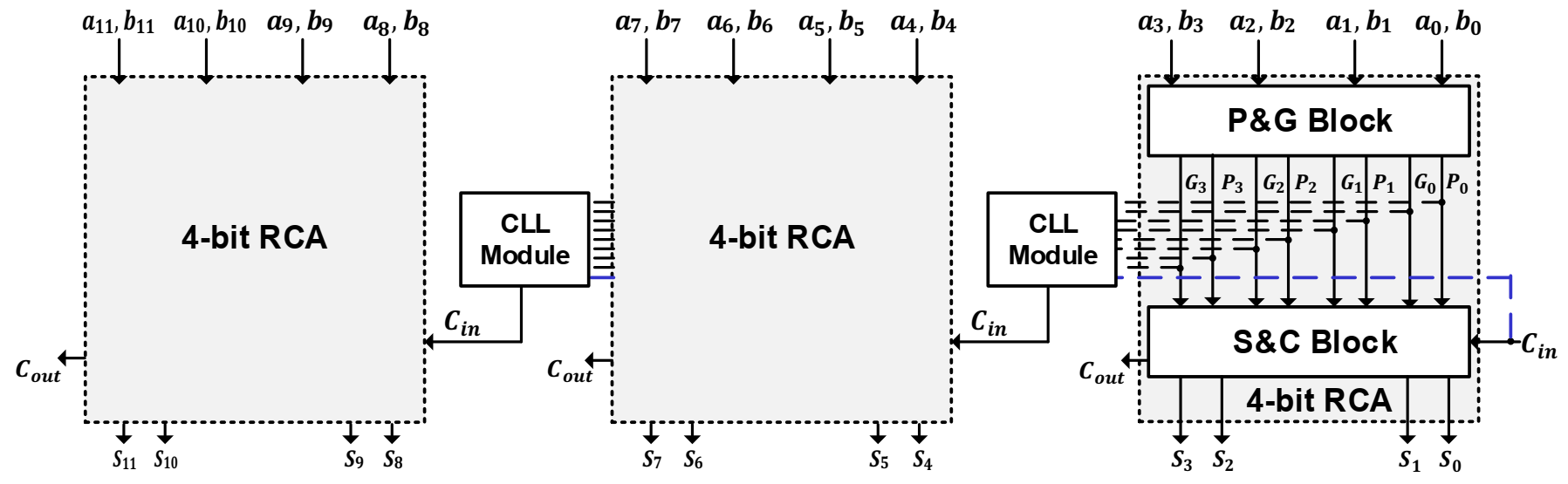
In the proposed architecture, RCA is divided into independent blocks where each block has four full adders. The initial cin, for each block other than the first one, will be generated with a CLL module, as shown in
Figure 1. Due to the proposed parallel architecture, the SUM bits computed by each block become dependent only on the carry-out of the preceding CLL module, which is constructed using the Boolean equation given in (1), where
and
are indicating the
propagate and generate signals of the previous block and can be computed by
and
, respectively. The sum-and-carry (S&C) block, shown in
Figure 1, is responsible for generating the final SUM and intermediate carries of the respective adder block, whereas the propagate-and-generate (P&G) block is used to provide the propagate and generate signals which are mutually shared between the CLL and S&C blocks.
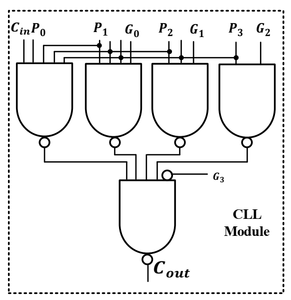
With the additional overhead of a CLL module, RCA is divided into parallel functioning blocks. However, each CLL will only generate carry-out after receiving the final output of the previous CLL module. In this way, each CLL is partially dependent on the preceding one for producing the final carry-out. It should be noted that this dependency is also present in CLA designs. However, this dependency between CLL modules can increase the latency of PRCA (
). Therefore, to reduce its impact, the logic diagram of the CLL module is designed using multiple-input NAND gates, as shown in
Figure 2. Hence, the first CLL module requires two-level gating to produce the output, whereas each consecutive CLL will generate a carry bit with an additional delay from two-level logic as compared with the preceding one. Therefore, the latency of CLL modules (
) is N/2-2, where N is the adder size, which is equal to 4k and where k = 1, 2, 3 … m. The overall delay of our design can be computed by Equation (2). It can be observed that apart from CLL, the delay caused by the last 4-bit RCA (
) block put additional overhead in the latency of PRCA. However, the overhead has a fixed constant value of 8 gates because the delay of an N-bit RCA is 2N. Hence Equation (2) can be further simplified to Equation (3).
2.2. PRCA with CSeA (PRCA-CSeA)
Since the latency of PRCA depends on CLL and the last 4-bit RCA block present in the design, the latency related to CLL for a given architecture cannot be further improved. While it is possible to reduce or eliminate the delay caused by the 4-bit RCA block by replacing it with a single adder-based CSeA design as shown in
Figure 3 [
7], the replacement of the last RCA block will only give a latency improvement of two gates. This is because each block has a uniform delay of eight gates and has a tendency to generate output with a delay difference of two gates caused by the respective CLL. Therefore, by replacing the last adder block with a CSeA gives an opportunity to immediately produce the four most significant output bits after receiving the carry bit from the respective CLL. Whereas, the second last block needs additional six gates of delay to produce the final outputs. Hence, the replacement of the last block shifts the critical path to the second last block, as shown in
Figure 4, where,
and
are representing the latency when one and two blocks of 4-bit RCA are replaced by CSeA.
Since the additional delay for PRCA is 6 gates and the latency difference between the consecutive CLL modules is 2 logic gates. Therefore, the delay overhead in Equation (2) can be accommodated by replacing the last three RCA blocks with CSeA because the difference in delays between the first and last CSeA module will be equal to 6 gates. In this scenario, there will be two possible critical paths with similar latency count. The first path ends with the final SUM output of the 4-bit RCA block present just before the chain of CSeA blocks, whereas the second path extends till final SUM out of the last CSeA block.
It should be noted that for multiple CSeA blocks, the need of a CLL module is limited to the first one, whereas the remaining CSeA blocks will produce output immediately after receiving the carry-out from the preceding block of CSeA. The general delay for all combinations of PRCA-CSeA is shown in Equation (4), where q is representing the number of CSeA blocks present in the design and q ≤ 4.
2.3. Proposed Self-Checking Approach
In conventional RCA and CSeA design, fault localization can be achieved by using self-checking full adder in which fault detection is independent of the propagated carry, as shown in [
7,
9]. In contrast to the conventional approaches, the proposed PRCA design has an additional CLL module. Therefore, in PRCA and PRCA-CSeA combination, the 4-bit RCA and CSeA designs are fault secure by using the previously reported approaches of [
7,
9]. For CLL modules, the self-checking is achieved by a TPRC approach because the cout generated by each adder block is equal to the carry bit generated by the respective CLL. The mismatch between these two carry bits will be indicated as fault by TPRC, as shown in
Figure 5, whereas the architecture of TPRC is self-checking with respect to its internal functionality as reported in [
13]. The proposed approach can detect multiple faults at a time, with the condition that each module should have a single event upset at a time.
3. Results and Benchmark
The aim of this research is to improve the delay of RCA with minimum area overhead. Therefore, the area overhead and latency of our proposed PRCA and PRCA-CSeA combination is compared with conventional RCA along with the CLA design.
The comparison results for this PRCA-CSeA design are obtained for three cases. In case one, only the last adder block is replaced with a CSeA block, whereas in cases two and three, the last two and three adder blocks are replaced. However, the replacement of the last three blocks with CSeA converts 16-bit PRCA to a linear CSeA design, with the only difference of a CLL module. Therefore, cases one and two are valid for adders more than or equal to 16-bit size, while case three is only recommended for adders having size ≥32-bit.
3.1. Area Overhead
The basic architecture of the PRCA design is similar to conventional RCA with the only difference being the addition of a CLL module. Therefore, the overhead caused by the CLL will define the hardware penalty of the PRCA design. The area of the PRCA can be reduced if the propagate and generate signals are shared between the respective full adders and CLL, as seen in
Figure 1. However, logic sharing is not possible in the case of self-checking PRCAs because the fault in the shared logic may have equal impact on the carry bit generated by the CLL and adder blocks. As a result, a fault in the CLL module cannot be detected because of common mode failure.
The area overhead of RCA, CLA, and PRCA is computed using complementary metal-oxide-semiconductor (CMOS) approach. The required number of transistor counts for different modules with and without self-checking, along with their required quantities of variously sized adders is shown in
Table 1. The main modules of PRCA are full adder, CLL, and TPRC, which is common with the PRCA-CSeA combination design. However, the PRCA-CSeA design has an additional overhead of AND, XOR and NOT gates along with its MUXs. The transistor count for TPRC and additional modules of PRCA-CSeA is taken from the previously reported approach in [
13,
14], as shown in
Table 1.
The overall area overhead of the proposed PRCA and PRCA-CSeA combination, without self-checking, is shown in
Table 2. It can be observed that the proposed 16-bit PRCA requires 16.25% area overhead as compared with a respectively sized RCA, whereas the area overhead is increased up to 20.31% for a 64-bit adder design. For case one of the proposed 64-bit PRCA-CSeA design, the required area penalty is 22.50% as compared with RCA, which further increased by 0.6% and 1.36% when implementing cases two and three of the proposed 64-bit PRCA-CSeA combination.
In comparison to CLA, which requires a fixed area overhead of 33.33% for all sizes as compared with RCA, it can be observed from
Table 2 that the transistor counts for our proposed 64-bit PRCA and case one’s PRCA-CSeA combination are 9.7% and 8.12% less than CLA, respectively.
In the case of fault-tolerant design, the proposed PRCA with self-checking requires 42.36% area overhead as compared with a 64-bit self-checking RCA design; this extends to 44.35% for case one’s self-checking PRCA-CSeA, as shown in
Table 2. The decreasing trend of transistor counts from case one to case three of our PRCA-CSeA combinations is because of the reduction in number of CLL and TPRC modules. The proposed 64-bit self-checking PRCA design requires 60.21% less area overhead as compared with a previously reported self-checking CLA [
15].
3.2. Latency
Latency is used to define the computational speed of digital circuits. The main problem of conventional RCA design is the carry-propagation chain, due to which the delay is equal to 2N. To avoid this problem, the concept of CLA was introduced in which latency is improved because, ideally, the carry required for the last full adder can be obtained directly without any additional delay. However, in actual conditions the latency of CLA is dependent on its architecture. For example, in a 4-bit CLA architecture, the adder is divided into 4-bit blocks and the internal carries are generated independently for each block. However, the final carry bit generated by each block will be served as an actual cin for the next block, due to which each consecutive block beyond the first will have an additional delay of two logic gates, which is similar to our proposed design. The overall latency of 4-bit CLA architecture can be computed using Equation (5).
The latency for our proposed PRCA and PRCA-CSeA combination can be computed by Equations (3) and (4), respectively. It can be observed from
Table 3 that the latency of our proposed 64-bit PRCA is reduced by 70.31% as compared with a respectively sized RCA design. However, our proposed PRCA offers 18.75% more latency count than that of CLA designs.
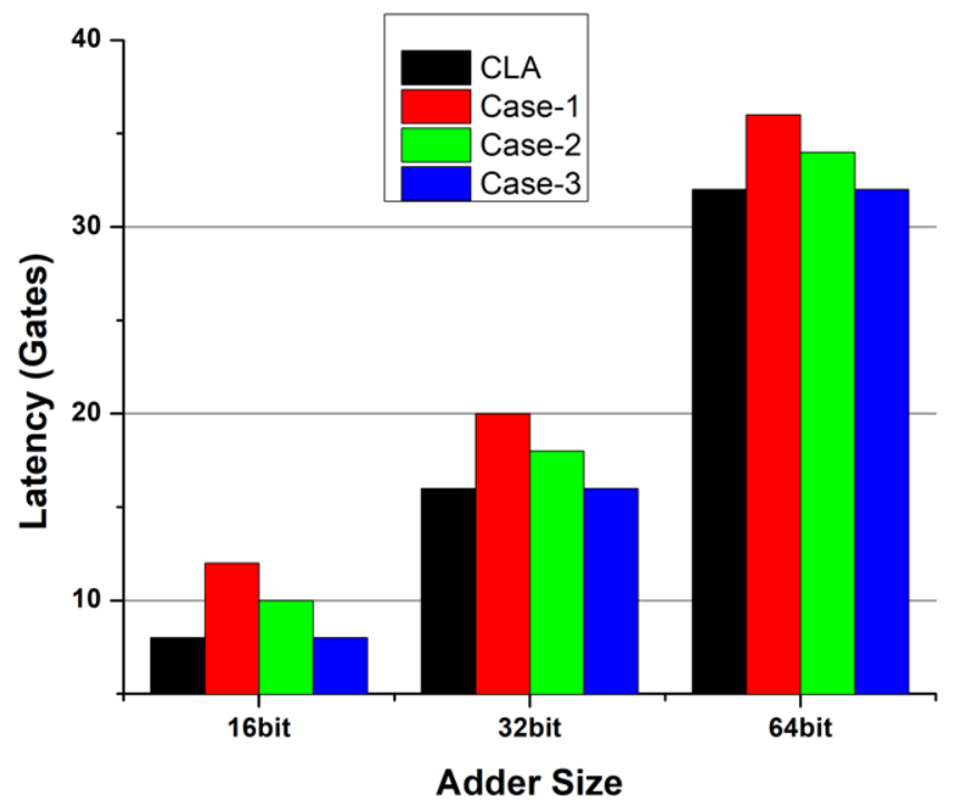
The latency difference between PRCA and CLA is reduced with the adoption of a PRCA-CSeA combination. For case one of our PRCA-CSeA combination, the latency difference is reduced to 12.50% for 64-bit designs as compared with CLA. The latency improvement for all three cases in comparison with CLA is shown in
Figure 6. It can be seen from the graph that the latencies of the proposed PRCA-CSeA and for CLA become equal in case three.
3.3. Simulation Results
The proposed design’s approach, along with conventional RCA and CLA designs, were implemented in a standard 180 nm process. Simulation results for power, delay, area, power–delay product (PDP), and power-delay-area product (PDAP) were obtained using a 1.8V supply. For the PRCA-CSeA combination, the simulation results are obtained for case three, which has similar latency to that of CLA.
The 64-bit PRCA design provided 43.81% delay efficiency as compared with a respective RCA design. The efficiency increased to 50.79% for the 64-bit PRCA-CSeA design, as shown in
Table 4. However, the delay of a 64-bit PRCA was 14.63% shorter than that of CLA, whereas the delay of PRCA-CSeA was similar to CLA.
In comparison with 64-bit RCA, the power consumption of PRCA and PRCA-CSeA was increased to 15.03% and 17.75%. However, the PDP for 64-bit PRCA and PRCA-CSeA was 35.37% and 42.17%, respectively, more efficient than RCA, as shown in
Table 5. Moreover, our proposed 64-bit PRCA and PRCA-CSeA provided 24.66% and 30.94% PDAP improvement as compared with RCA. The PDAP of the proposed designs was 10.28% and 17.77% more efficient than CLA. The simulation results validated the performance efficiency of our proposed design when compared with RCA and CLA.
4. Conclusions
In this paper, parallel architectures for RCA with self-checking and fault localization abilities were presented. The primary idea was to divide an N-bit RCA into 4-bit concurrent blocks. Each block was independent in terms of processing, whereas the actual cin for each block was generated via a CLL module present before each.
The delay of the proposed 64-bit PRCA was reduced by 43.81% as compared with RCA. However, the latency was 14.63% more than CLA. To minimize the difference in delay between CLA and PRCA, the last 4-bit adder block of PRCA was replaced by CSeA. It was found that the delay of CLA and PRCA-CSeA combination are made equal by replacing the last three blocks of PRCA with CSeA.
In terms of area overhead, the proposed 64-bit PRCA required 20.31% more area than the conventional RCA, which is 9.7% lower than 64-bit CLA. The area overhead of PRCA-CSeA combination depended on the number of CSeA modules present in the design. For case one, of 64-bit size, the area overhead was increased by 22.50% as compared with conventional RCA, whereas an additional overhead of 0.6% and 1.36% was required for the implementation of cases two and three, respectively. The power consumption of the proposed design also increased with the area overhead. However, the PDAP results showed that the 64-bit PRCA and PRCA-CSeA were 24.66% and 30.94% more efficient than RCA.
Self-checking and fault localization are mainly achieved by a combination of self-checking full adders, in which fault detection is independent of the propagated carry and the TPRC, itself responsible for checking the carry output of the CLL. The proposed design can detect multiple faults at once, with the condition that a single module should not have more than one fault at a time. The area of the proposed 64-bit self-checking PRCA is 42.36% more than the respective self-checking RCA design. For similar adder sizes the area overhead for case one is 44.35% more than self-checking RCA. It should be noted that our proposed self-checking PRCA design requires 60.21% less area than a previously reported self-checking CLA.
Author Contributions
Conceptualization, M.A.A.; Formal analysis, M.A.A. and B.W.; Methodology, M.A.A.; Project administration, A.B.; Supervision, A.B.; Writing—original draft, M.A.A.; Writing—review & editing, A.B. and B.W. All authors have read and agreed to the published version of the manuscript.
Funding
This work was supported by NPRP from the Qatar National Research Fund (a member of Qatar Foundation) under Grant NPRP11S-0110-180246.
Conflicts of Interest
The authors declare no conflict of interest.
References
- Lala, P.K.; Kumar, B.K. An architecture for self-healing digital systems. J. Electron. Test. 2003, 19, 523–535. [Google Scholar] [CrossRef]
- Smith, J.E.; Lam, P. Theory of totally self-checking system design. IEEE Trans. Comput. 1983, C-32, 831–844. [Google Scholar] [CrossRef] [Green Version]
- Mukherjee, A.; Dhar, A.S. Real-time fault-tolerance with hot-standby topology for conditional sum adder. Microelectron. Reliab. 2015, 55, 704–712. [Google Scholar] [CrossRef]
- Senthilpari, C.; Singh, A.K.; Diwakar, K. Design of a low-power, high performance, 8× 8 bit multiplier using a Shannon-based adder cell. Microelectron. J. 2008, 39, 812–821. [Google Scholar] [CrossRef]
- De Dinechin, F.; Didier, L.S. Table-based division by small integer constants. In International Symposium on Applied Reconfigurable Computing; Springer: Berlin/Heidelberg, Germany, 2012; pp. 53–63. [Google Scholar]
- Kito, N.; Takagi, N. Concurrent error detectable carry select adder with easy testability. IEEE Trans. Comput. 2019, 68, 1105–1110. [Google Scholar] [CrossRef]
- Akbar, M.A.; Lee, J.A. Self-checking carry select adder with fault Localization. In Proceedings of the 2013 Euromicro Conference on Digital System Design, Los Alamitos, CA, USA, 4–6 September 2013; pp. 863–869. [Google Scholar]
- Moradian, H.; Lee, J.A.; Hashmi, A. Self-repairing radix-2 signed-digit adder with multiple error detection, correction, and fault localization. Microelectron. Reliab. 2016, 63, 256–266. [Google Scholar] [CrossRef]
- Akbar, M.A.; Lee, J.A. Self-repairing adder using fault localization. Microelectron. Reliab. 2014, 54, 1443–1451. [Google Scholar] [CrossRef]
- Ramkumar, B.; Kittur, H.M. Low-power and area-efficient carry select adder. IEEE Trans. Very Large Scale Integr. Syst. 2011, 20, 371–375. [Google Scholar] [CrossRef]
- Chirca, K.; Schulte, M.; Glossner, J.; Wang, H.; Mamidi, B.; Balzola, P.; Vassiliadis, S. A static low-power, high-performance 32-bit carry skip adder. In Proceedings of the Euromicro Symposium on Digital System Design, Rennes, France, 31 August–3 September 2004; pp. 615–619. [Google Scholar]
- Pai, Y.T.; Chen, Y.K. The fastest carry lookahead adder. In Proceedings of the DELTA 2004. Second IEEE International Workshop on Electronic Design, Test and Applications, Perth, WA, USA, 28–30 January 2004; pp. 434–436. [Google Scholar]
- Vasudevan, D.P.; Lala, P.K.; Parkerson, J.P. Self-checking carry-select adder design based on two-rail encoding. IEEE Trans. Circuits Syst. I Regul. Pap. 2007, 54, 2696–2705. [Google Scholar] [CrossRef]
- Akbar, M.A.; Wang, B.; Bermak, A. Self-repairing hybrid adder with hot-standby topology using fault-localization. IEEE Access 2020, 8, 150051–150058. [Google Scholar] [CrossRef]
- Valinataj, M. Enhanced multiple-error resilient carry look-ahead adders through new customized fault-tolerant voters. Microelectron. Reliab. 2019, 96, 7–20. [Google Scholar] [CrossRef]
| Publisher’s Note: MDPI stays neutral with regard to jurisdictional claims in published maps and institutional affiliations. |
© 2021 by the authors. Licensee MDPI, Basel, Switzerland. This article is an open access article distributed under the terms and conditions of the Creative Commons Attribution (CC BY) license (https://creativecommons.org/licenses/by/4.0/).


