Article

Case Study on Integrated Architecture for In-Memory and In-Storage Computing

1
Department of Electrical Engineering, Seoul National University, Seoul 08826, Korea
2
Department of Information and Communication Engineering, Inha University, Incheon 22212, Korea
*
Author to whom correspondence should be addressed.
Electronics 2021, 10(15), 1750; https://doi.org/10.3390/electronics10151750
Submission received: 15 June 2021 / Revised: 16 July 2021 / Accepted: 17 July 2021 / Published: 21 July 2021
(This article belongs to the Section Computer Science & Engineering)

Abstract

:
Since the advent of computers, computing performance has been steadily increasing. Moreover, recent technologies are mostly based on massive data, and the development of artificial intelligence is accelerating it. Accordingly, various studies are being conducted to increase the performance and computing and data access, together reducing energy consumption. In-memory computing (IMC) and in-storage computing (ISC) are currently the most actively studied architectures to deal with the challenges of recent technologies. Since IMC performs operations in memory, there is a chance to overcome the memory bandwidth limit. ISC can reduce energy by using a low power processor inside storage without an expensive IO interface. To integrate the host CPU, IMC and ISC harmoniously, appropriate workload allocation that reflects the characteristics of the target application is required. In this paper, the energy and processing speed are evaluated according to the workload allocation and system conditions. The proof-of-concept prototyping system is implemented for the integrated architecture. The simulation results show that IMC improves the performance by 4.4 times and reduces total energy by 4.6 times over the baseline host CPU. ISC is confirmed to significantly contribute to energy reduction.

1. Introduction

Recently, there has been growing interest and demand for artificial intelligence and immersive media. These applications require high performance devices to process massive data. However, it is difficult to compute and transfer such large amounts of data in the traditional von Neumann architecture because it consumes significant power and dissipates heat energy as Moore’s Law and Dennard scaling reach physical limits. It is known that data access and movement are the main bottleneck of processing speed, and they consume more energy than computing itself [1]. Thus, many studies about near data processing are ongoing to overcome these challenges [2,3].
Near data processing is applicable not only in traditional memory, such as SRAM [4,5] and DRAM [2,6,7,8,9,10], but also in emerging memory, such as PCM [11], STT-MRAM [12], and ReRAM [13]. There are also various attempts to reduce the data movement overhead by computation offloading to storage devices [3,14,15,16]. However, real-world applications are composed of complex and diverse tasks, and thus, there is a limit to solving the problems with an individual device-level approach. In this paper, the requirements of tasks for real application scenarios are analyzed in terms of task partition and the data movement overhead. By providing various options for near data processing in consideration of the characteristics of each task that composes an application, opportunities to reduce the data movement overhead are explored at the architectural level.
  • This paper makes the following contributions:
  • The requirements of the task are analyzed from the memory and storage points of view.
  • An integrated architecture for in-memory and in-storage computing is proposed, and its implementation is verified on a prototyping system.
  • Possible performance improvement is shown in terms of execution time and energy.

2. Background and Related Work

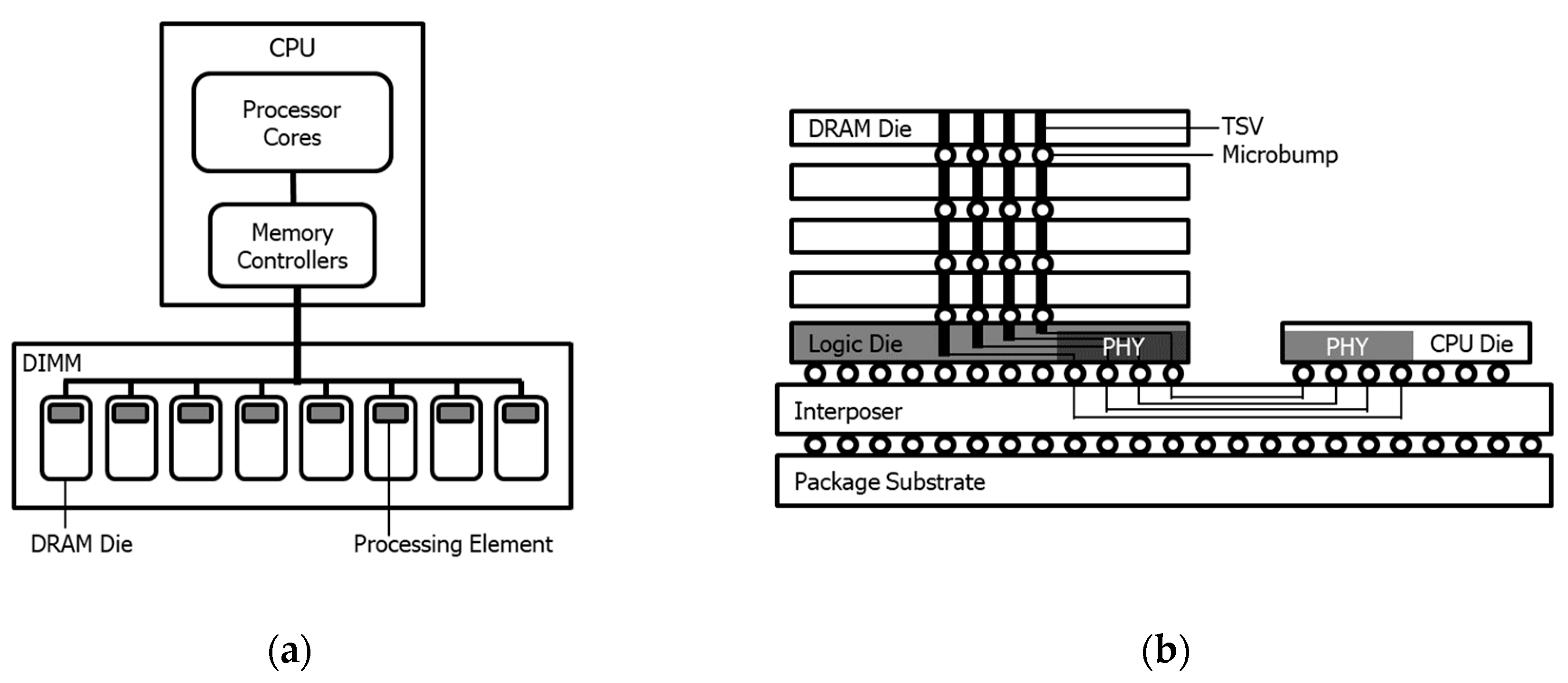
2.1. In-Memory Computing

In-memory computing (IMC), also known as processing in-memory (PIM), is a paradigm that places processing elements near or inside the memory in order to obtain fast memory access and high bandwidth. Among the various types of memory, this paper focuses on in-memory computing for DRAM, which is most widely used and has high density. There are two categories of in-DRAM computing depending on the package and module assembly of the DRAM chip: computation in two-dimensional (2D) planar DRAM, and computation in three-dimensional (3D) stacked DRAM. In 2D planar DRAM, processing elements reside in the DRAM die as shown in Figure 1a. Since data travel through on-chip inter-connection on the DRAM die, it is free from off-chip IO constraints, and also it can achieve high parallelism by exploiting the bit-line of the subarray, row buffer, and internal data line [2,6]. However, there are some difficulties in computing in 2D planar DRAM. Because the DRAM manufacturing process is optimized for low cost and low leakage, only simple logic can be placed, due to the bulky and slow transistors. The standard logic process is optimized to deal with complex logic functions, but requires frequent refresh operations, due to the current leaky characteristic. This leads to high power consumption and poor performance. In order to overcome these drawbacks, there have been attempts to add separate chips for processing elements over the 2D planar DRAM chip in the dual-inline memory module (DIMM) [7,8]. However, additional assembly process is required, and cost is consequently increased. On the contrary, 3D stacked DRAM, such as high bandwidth memory (HBM) and hybrid memory cube (HMC), can use the DRAM process and standard logic process together because they pile up more than two dice. Therefore, more complex processing elements can be located on the base die with the standard logic process as shown in Figure 1b [9,10]. Even though the physical interface (PHY), through-silicon via (TSV), and IEEE1500 area for test pins and circuits occupy the base die, there is still extra space that can be used for other purposes.

2.2. In-Storage Computing

For in-storage computing (ISC), some computations are offloaded to the storage device. There was a study in which a hard disk drive (HDD) used a processor to compute offloaded tasks for ISC [14]. However, HDDs were quickly replaced by solid-state drives (SSDs), after SSDs were introduced. The conventional SSDs do not process data, even though they have an embedded processor. The internal structure of the SSD is shown in Figure 2. The SSD consists of non-volatile NAND flash chips that do not lose data regardless of power-off, and an embedded processor, such as the ARM processor, to manage the firmware, such as the flash translation layer (FTL). Even if the conventional SSD is not designed for in-storage computing, it is capable of computation because it already has an embedded processor. The main concept of SSD-based ISC is that the SSD is regarded as a small computer with an embedded processor to run programs within the storage device. ISC increases the system performance because a storage device can handle the tasks in parallel with the host CPU. It also decreases data movements if the data are selectively transferred to host the CPU after processing within the storage device. This lowers the IO latency and improves the energy efficiency.
If the tasks, such as query processing [17], list intersection [18], scan and join [19], Hadoop MapReduce [20], and search engine [18] are offloaded to an embedded processor in SSD, it improves the processing speed and energy efficiency. Not only did other studies employ an embedded processor, but they also introduced additional implementations of FPGA [21] or GPU [22] in the SSD. However, they have significant disadvantages, such as modification of the SSD structure, resulting in additional costs.

2.3. Integrated Solution of In-Memory and In-Storage Computing

The integration of in-memory and in-storage computing is an architecture where IMC and ISC are applied simultaneously in order to improve the processing speed and energy efficiency of applications. However, the structure with ReRAM-based IMC inside the SSD performing ISC [23] cannot avoid IO bottlenecks because the data have to be delivered into the SSD for offloaded task operations. Another hybrid architecture, which consists of the memory channel network (MCN) DIMM [24] for IMC and Samsung Smart SSD for ISC, needs more space in the buffer die in the DIMMs for the MCN processor. The architecture manufacturing cost increases as explained in Section 2.1 because it also has additional chip implementation in the 2D planar DRAM. Other hybrid architectures, such as near-memory and in-storage FPGA acceleration architectures [25] require 3D stacked memory in the SSD to implement FPGAs rather than the conventional 2D planar DRAMs. Thus, additional costs are required, such as the example of the SSD with a GPU in Section 2.2.

3. A Case Study on Integrated Architecture for In-Memory and In-Storage Computing

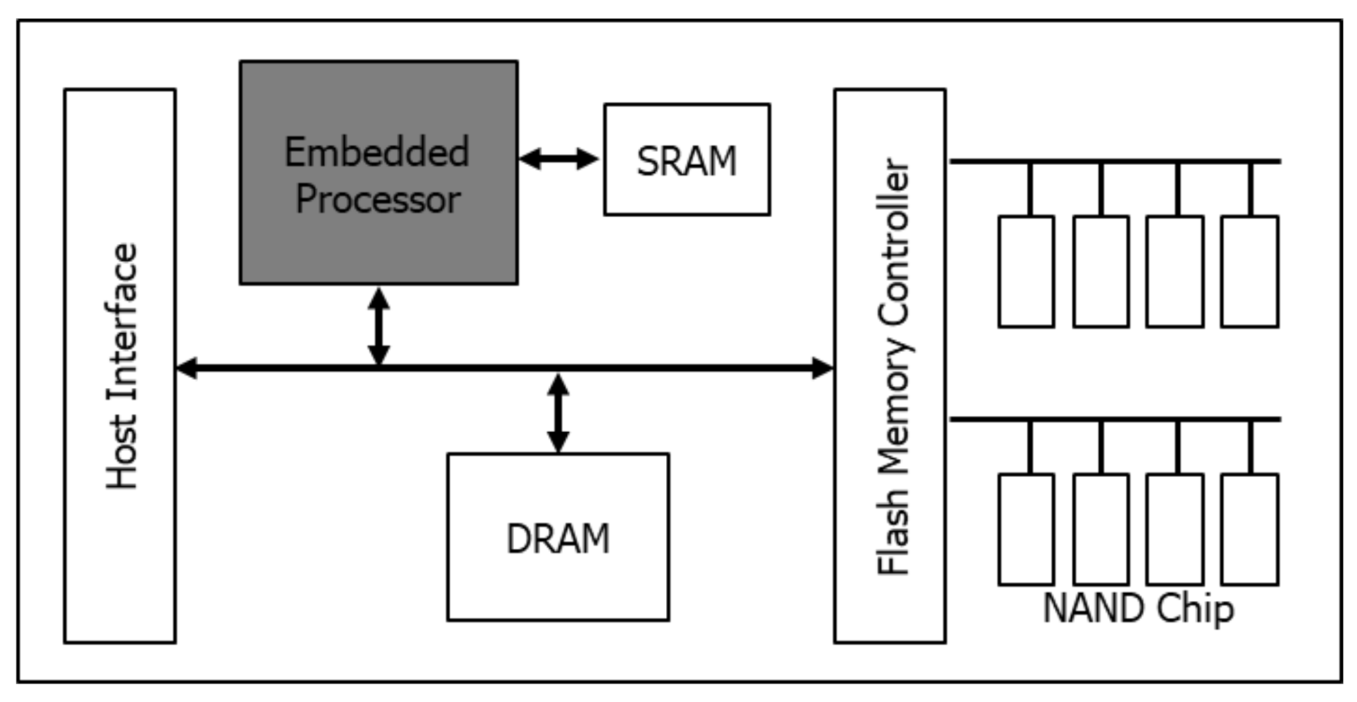
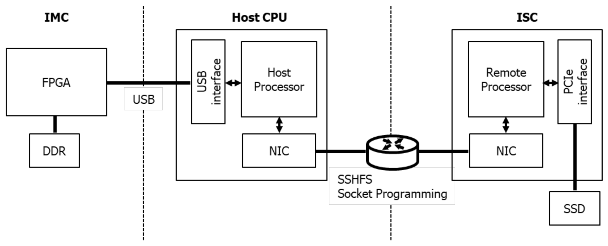
3.1. Prototype Platform

Figure 3 shows the prototype platform to test the proposed hybrid architecture. The host CPU is on the host PC, and it is connected with the FPGA that acts as an IMC via a USB interface. The storage server for modeling ISC is connected through a network. The purpose of this platform is to evaluate the performance of an application in a hybrid architecture quickly, focusing on data movement. Because there is no commercial integrated solution of in-memory and in-storage computing specification, the prototype was implemented using configurable commodity devices in order to deal with various requirements. To support the hybrid architecture effectively, FPGA is adopted for IMC implementation to easily modify the logic circuits of the base die. The Xilinx Zynq UltraScale+ MPSoC ZCU102 Evaluation Kit is used where the DDR memory corresponds to the DRAM die and the programmable area corresponds to the logic die. The accelerator of IMC is developed on Xilinx Vivado, whereas the firmware is programmed with the Xilinx Vivado SDK. To model the interposer connected between the host CPU and memory, a high-speed USB is used for the host PC and FPGA connection. In terms of the ISC operation, it can be prototyped using a low-performance computer with large storage space. To mimic the IO constraints of SSDs, the host PC and ISC are connected through the network and mounted storage server and SSH file system (SSHFS) to access large data files. It transfers commands and data to the storage server with socket programming.

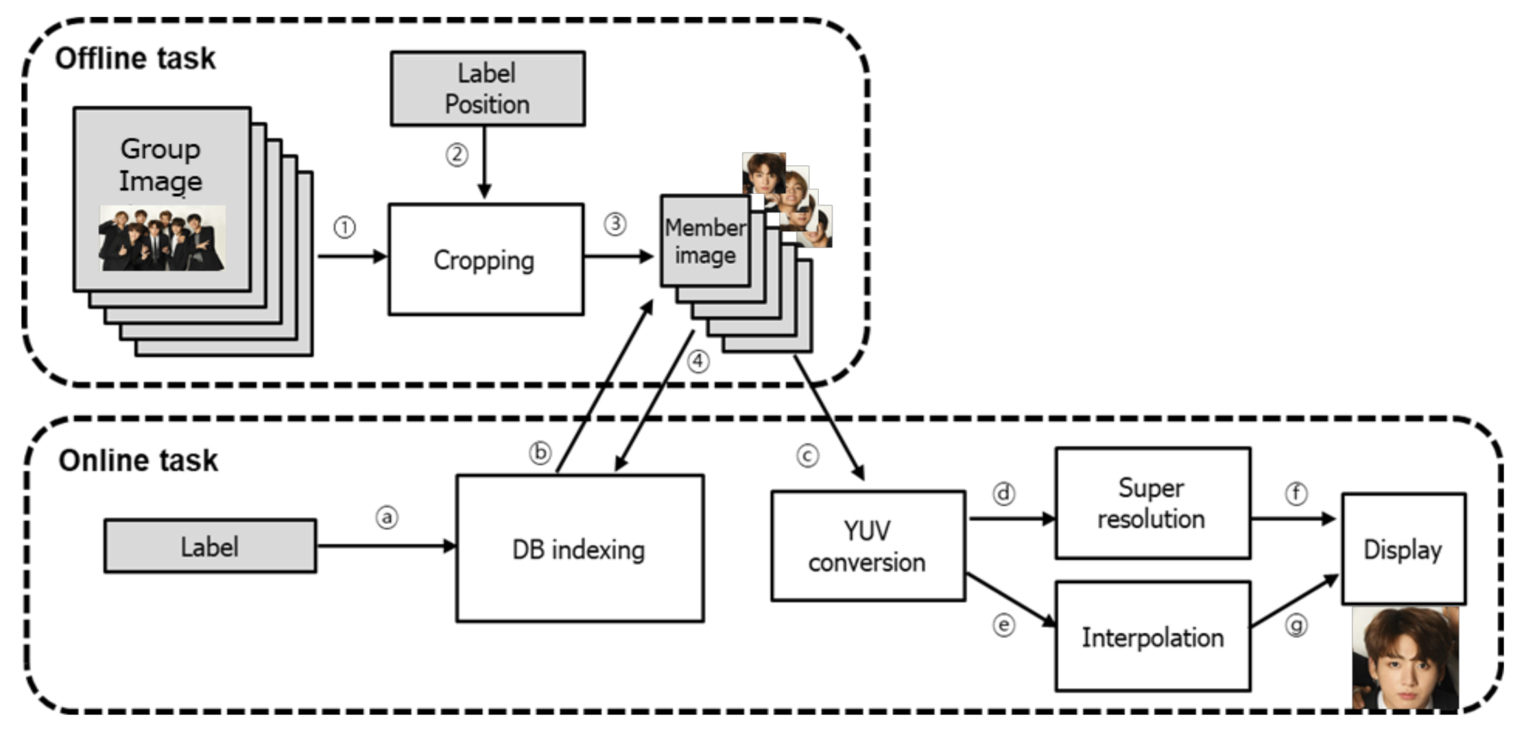
3.2. Workload Analysis from the Perspective of Data Accesses

In this paper, a focus fancam is used as a case study application. In this scenario, the series of tasks are divided into two phases: off-line and on-line. The first off-line phase prepares data prior to the user request. Here, data are managed in the background, and there are no urgent deadlines. Therefore, it does not require high-performance computing but the amount of handling data in the file format is very large. On the other hand, in the second on-line phase, the user request is processed in real time. Therefore, it needs powerful computing capability and a high memory bandwidth. Focus fancams are re-edited videos that focuses on the favorite celebrity. The original video is reproduced in hundreds of different versions, securing a wide user base. Using auto highlight technology, artificial intelligence (AI)-based algorithms generate videos or images focused on specific members in an idol group. As a case study of this paper, labeled-image-based focus picture editing is used. Input data are images of a K-pop group, labels, and position information, whereas output data are cropped images of each member in the group. The group image is a JPEG file in which all members appear together. The label is text data, which is the unique name of each member, and it is used as a key to the index table. The position is represented as a coordinate that indicates where a particular member is in the group image. The member image is a cropped picture, according to the member position information from the group image. Users can view their favorite member images originated from group images, and sometimes edit and share them with other users. Among the tasks of the focus fancams application, a super resolution (SR) technique plays an important role. It enhances the resolution of small cropped images by means of the deep learning algorithm.
Figure 4 shows a focus fancam application scenario. White and gray boxes indicate tasks and data, respectively. Numbers with arrows indicate the data flow of the off-line phase. At first, it reads the group images (①) and obtains labels and position information (②) of each member in the group images. The JPEG files are decoded and then regions of interest are cropped, such as the face. The cropped images are encoded back to JPEG. For database (DB) indexing, it updates data (④) in the index table with each member’s names as keys and the file paths of the cropped image as values. Data movement of group images take place in proportion to the number of files stored. Since the number of labels, positions and member image files increase in proportion to the number of people in the group images, there is a lot of data movement. The cropping and update tasks are performed on the background whenever new group images come into storage. They do not have strong latency constraint. Letters with arrows of Figure 4 indicate the data flow of the on-line phase. It reads label (ⓐ), which is a member’s name. It retrieves the index table with the label to obtain the corresponding file path (ⓑ). It reads the member’s image (ⓒ) from the found file path. Here, the image is divided into Y and UV color components. Upscaling is executed with different algorithms according to color components to reduce the overall execution time. For the visually sensitive Y component, convolutional neural network (CNN) based SR is performed [26] (ⓓ), which gives good performance but is computationally expensive. For the UV components, the least neighbor interpolation algorithm is applied (ⓔ). Since there is no dependence between Y and UV color channels, it is possible to execute those algorithms in parallel. Then, it brings the data which are upscaled Y (ⓕ) and upscaled UV (ⓖ). It rearranges the separately upscaled Y and UV together, converts the color space from YUV into RGB, and finally displays the favorite member’s upscaled image. Data movement in the on-line phase is less than that in the off-line phase because it only needs to handle the user’s request. However, YUV conversion, Y-SR, and UV-interpolation tasks strongly require low-latency computations because they immediately produce the results upon user request.
Table 1 summarizes the requirements for data movement in Figure 4. The second column represents the data flow of the main tasks, whereas the third and fourth columns represent the data unit size and latency requirement in each dataflow, respectively. The cropping task of the focus fancam has data movement of ①, ②, and ③. The data unit size of a group image (①) is as large as 1 K or 2 K resolution and is assumed to be 150 KB on average. The data unit size of the label, which comprises unique key and position information, which is x–y coordinates of the picture (②), is just 12 bytes. The member image (③) also has a small data unit size of around 20 KB. The index table update needs the label and member image file path data (④), and its data unit size is 64 bytes of string format. The index table retrieval task has data movement of ⓐ and ⓑ, where the label (ⓐ) needs 4 bytes of a unique key, and the file path (ⓑ) needs 64 bytes of the string. The YUV conversion task has data movement of ⓒ, ⓓ, and ⓔ. Here, the unit size of the member image file (ⓒ) is assumed to be 20 KB. The luminance Y (ⓓ) and UV component (ⓔ) need 256 KB and 128 KB, respectively, because a 256- by 256-pixel image is used with 4:2:0 chroma subsampling. The Y- SR task and the UV-interpolation task have data movements of ⓓ, ⓕ and ⓔ, ⓖ, respectively. The unit size of the upscaled Y (ⓕ) is 1 MB, due to a scale factor of 2, whereas the upscaled UV (ⓖ) requires 512 KB because of subsampling.

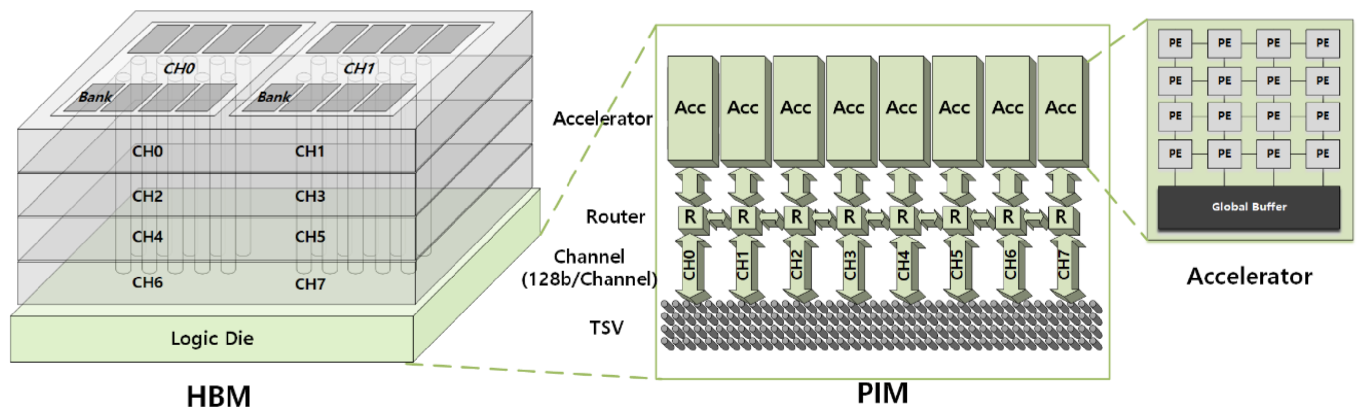
3.3. Application to Integrated In-Memory and In-Storage Computing

In this paper, an integrated framework for in-memory and in-storage computing architecture is proposed. IMC and ISC are incorporated into a single system for the target application, i.e., focus fancam as shown in Figure 5. In this architecture, there are two candidate devices: IMC and ISC for task offloading. Therefore, the device to be offloaded should be appropriately selected, according to the task characteristics. Gray boxes indicate data, whereas white boxes indicate the computing resources of each device. The host CPU is responsible for offloading tasks to IMC and ISC and obtaining the results back from them. This central orchestration is a relatively simple operation. Thus, the host CPU can afford to provide additional computing resources for the remaining tasks that are un-offloaded. IMC processes the data stored in the DRAM, taking advantage of being close to the data. The distance of the data movement is short, due to the TSV connection and thus, the latency penalty caused by going through the cache and memory controller can be reduced. Since the host CPU and IMC are connected with a through silicon interposer (TSI), energy consumption can be reduced because the capacitive loading is less than that of the off-chip interconnection used in the general DDR DRAM. The accelerator, implemented as a computing unit in a logic die, can improve the overall performance by utilizing parallelism. In the case of ISC, the embedded processor with a buffer memory computes the data, which are stored in the NAND flash chip, instead of passing them all to the host CPU. After the processing of ISC, only the processed result moves to the host CPU, and it significantly reduces IO operations as well as the bottleneck delay caused by IO requests. In addition, it is possible to perform the tasks energy efficiently, due to the low power characteristic of the embedded processor of ISC.
As shown in Table 1, the tasks of the target application have different characteristics, and appropriate offloading strategies are required. Among the tasks of the focus fancam application, cropping does not need to have low latency, but it has large data movement. Therefore, the task is offloaded to ISC. The update data for the index table are stored in the storage device to keep the persistence characteristics of the database. Thus, it is appropriate for this task to be offloaded to ISC, as well. However, the YUV task requires less data movement but needs low-latency computation. SR of the Y component is also computation intensive and suitable for IMC. In particular, for SR, it is appropriate to use the accelerator instead of general processors. For the YUV color space, each color component is independent and thus, operations with YUV can be easily performed in parallel. Moreover, interpolation of UV component is less computation intensive. Therefore, it can be performed simply on the host CPU. Finally, the host CPU puts together the independently upscaled Y and UV components from each device. In terms of the data movement of Figure 4, the data flow of ①, ②, ③, and ④ in the off-line phase, and the data flow of ⓐ, ⓑ and ⓒ in the on-line phase need a storage IO interface. In the mapping of Figure 5, ①, ②, ③, ④ and ⓑ are performed inside the device of ISC. Data flow ⓐ and ⓒ need an off-the-device interface between a host CPU and storage. Data flow ⓓ, ⓔ, ⓕ, and ⓖ do not require a storage IO.

4. Experimental Results

4.1. Experimental Environment

In this paper, i7-7700K is used for a host CPU. The host-CPU-only system acts like a baseline system. Figure 6 shows the IMC architecture used in this paper. The IMC adopts systolic arrays to execute parallel multiply and accumulate operations (MAC) on the logic die like other CNN accelerators, such as EYERISS [27], but the IMC processes data in memory through TSVs of the HBM2 structure. On the base logic die, there are eight accelerators, and each accelerator consists of 168 processing elements (PEs) and 108 KB of a global buffer. PEs communicate with each other through network on-chip (NoC). nn_dataflow [28] is used to evaluate the performance of accelerators. The area and energy affected by the SRAM (global buffer) size are obtained through CACTI [29]. It is known that CACTI has an accuracy of less than 12% on average, compared to SPICE. For remote accesses to other channels, the NoC power is estimated using ORION 2.0 [30]. The Dram Power tool [31] is used to compare run time and energy according to data movement. For the ISC, ARM Cortex R5 is assumed. The operation of ISC, where the offline phase is mainly performed, is measured through Gem5 [32]. While performing a cropping task, the decoding (from JPEG to BMP) of large size images requires 16,055 M operations, whereas the encoding (from BMP to JPEG) of cropped small size images requires 40 M operations. For the comparison of DRAM energy in Gem5 [32] environment, i7-7700K uses the IDD value of DDR4 16 GB 2400 Mhz × 64 (8 Devices/rank, 2 Ranks/Channel, MT40A1G8 Data Sheet), and Cortex R5 uses the LPDDR4 8 Gb 4266 ×32 (2 Devices/rank, MT53E256M32D2 Data Sheet) IDD value. The SSD energy is calculated using the read/write energy of the Samsung SSD 980 PRO (PCIe Gen4) data sheet.

4.2. Processing Time and Energy Comparison for On-Line Phase

In the on-line phase of focus fancam scenarios, the execution time is measured in the proof of concept with the help of the nn_dataflow simulator. A total of 100 images of the members are cropped during the off-line phase in advance, according to the user favorite member requests. Table 2 shows the runtime and energy comparison for four main operations of the on-line phase. The baseline denotes running the focus fancam application on the CPU-only system, whereas the proposed IMC denotes the host CPU-IMC hybrid architecture for the on-line phase. The host CPU uses DDR4, whereas the IMC uses HBM2. Energy and time measurement conditions are 100 MB read from memory and 25 MB write. The row page hit ratio is applied as 80%. The HBM2 IDD data sheet has not been released. Therefore, the IDD value of HBM2 is estimated based on the IDD data sheet of DDR4. Since HBM2 has a wider data width compared to DDR4, it can be predicted that the data circuit will also increase. Considering that part, we estimate the standby current of HBM2 to be twice that of DDR4. Toggle energy of TSV is added to IDD4W/R. IO Interposer capacitance is used instead of PCB. HBM2’s TSV capacitance is 47.5 fF/1 stack [33] and TSV output loading is 100 fF [34]. The IO interposer capacitance is 855 fF/5 mm [35]. The second and third columns represent the execution time, whereas the fourth and fifth columns represent energy. Among tasks for the on-line phase, DB retrieval is performed in ISC. However, it takes very little time of 12 us on average and thus, is not shown in Table 2. YUV conversion is performed on the host CPU in both systems of the baseline and proposed IMC. SR of the Y component and the interpolation of the UV components are performed in parallel. UV interpolation runs on the host CPU in both cases. For SR using the context-preserving filter reorganization very deep convolutional network for image super-resolution (CPFR-VDSR) network, the runtime of the baseline is 2307.6 ms and its power is 113.1 W. Thus, it consumes 260,691 mJ of energy. On the other hand, the SR runtime of IMC is 72.8 ms, and its power is just 4.62 W. Therefore, it consumes 336 mJ energy. Both runtime and energy are significantly reduced. In terms of data movement, in the proposed IMC, the runtime of the data movement is reduced by 88%, whereas energy is reduced by 21% because an interposer is used instead of PCB. Due to the improved runtime and energy in SR and data movement, in the proposed IMC, the total runtime and energy are reduced by 77.5% and 78.4%, respectively.
For performance comparison, instead of the baseline of Table 2, which is a combination of DDR4 and CPU, the efficiency under different system conditions where an accelerator is used with DDR4 is measured. In Table 3, four system conditions are summarized. D1 uses one DDR4 chip with an accelerator, whereas D8 uses 8 DDR4 chips to increase the number of channels to a level similar to HBM2. H1 denotes an accelerator with a 1-channel HBM2, whereas H8 denotes an 8-channel HBM2. DRAM devices have different numbers of IO pins. DDR4 and HBM2 have 8 and 128 IO pins/channel, respectively.
Figure 7 shows an efficiency and throughput when SR is performed. For the throughput, GOPS (Giga Operation Per Second) is used, whereas the GOPS/W, which calculates GOPS that can be processed per watt for efficiency, is used to measure the efficiency. For H8, the throughput and efficiency are 1012 GOPS and 219 GOPS/W, respectively. H8 shows a clear performance advantage, compared to D8. The CPFR-VDSR used for SR is a small network, and its data reuse ratio is quite low. Therefore, it is obvious that reducing the access latency of 3D stacked memory has a huge impact on performance improvement. Figure 8 shows the energy efficiency results (GOPs/W) for different kinds of popular neural networks. The IMC-based accelerator improves average energy efficiency by 1.78× compared to the accelerator, which needs off-chip memory access, such as Eyeriss [27]. The average energy efficiency of Eyeriss is 118 GOPs/W and that of the proposed architecture is 210 GOPs/W.

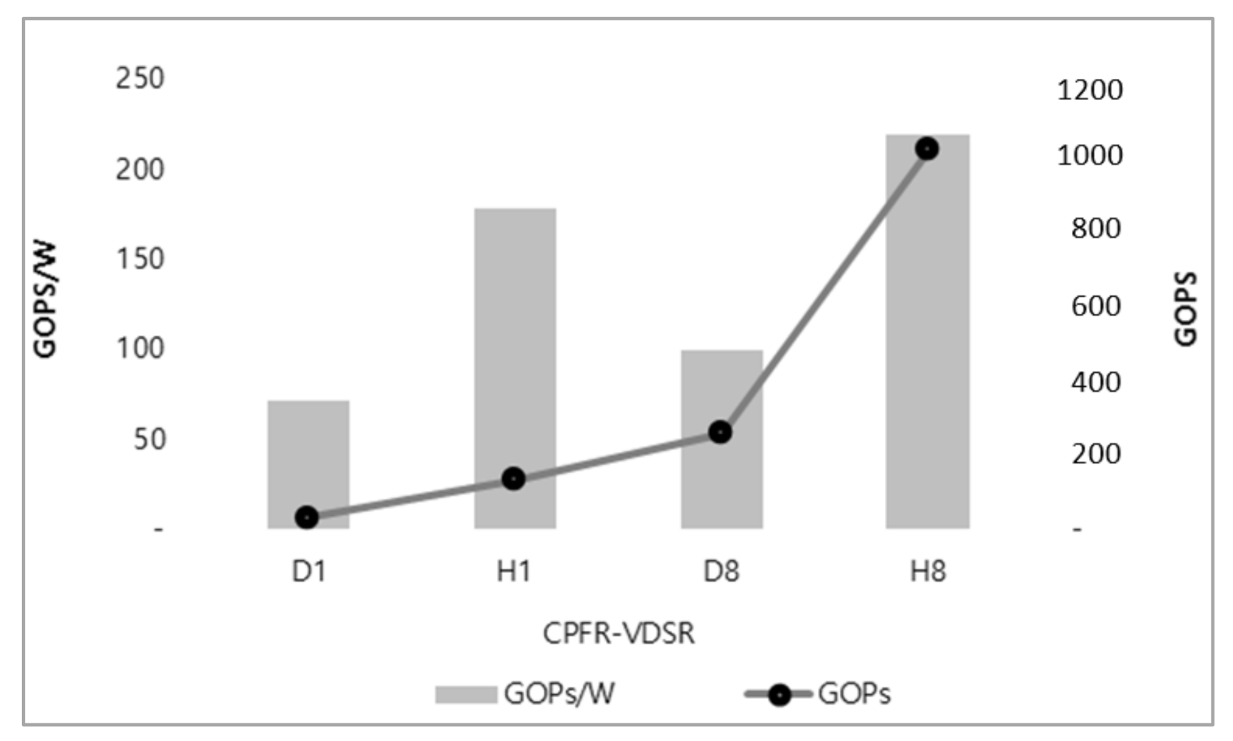
4.3. Processing Time and Energy Comparison for Off-Line Phase

The off-line phase of the focus fancam consists of a couple of tasks. The images are decoded from JPEG to BMP format and cropped to a 256 × 256 image. The cropped images are encoded back to JPEG. With a new key–value pair, the cropped JPEG files are stored in the DB of SSD. The off-line phase does not demand a tight latency requirement. Therefore, energy minimization is a main concern. In the example scenario, it is assumed that there are 1000 group images per each group and that there are 20 groups in total. In average, the group images are 1 K or 2 K resolution having the size of 150 KB. Each group image has five members. The size of a cropped member image is about 20 KB.
Table 4 shows the specification of the processors in the host CPU and ISC. i7-7700K in the host CPU is a baseline system; it is composed of 4 cores and its speed is 4.4 GHz. It has 6.05 CoreMark/Mhz performance and 1.24 GOPS/W power efficiency. When 140 GOPS is operated, it consumes 113 W of power. Meanwhile, Cortex R5 in the proposed ISC is composed of 2 cores and its speed is 1.4 Ghz. It has a 3.47 CoreMark/Mhz performance and a power efficiency of 5.61 GOPS/W. The 12.8 GOPS consumes 2.3 W of power.
When cropping a small image from each image, the number of operations and DRAM access energy are compared. This off-line task is compared with the case of the CPU and the case of the ARM in the SSD. In Table 5, in the case of one image encoding and conversion, i7-7700K of a baseline system consumes 15.4 J, whereas Cortex R5 in the proposed ISC consumes 3.6 J. Thus, the energy is reduced by 76.6%. Here, the energy for processing and DRAM is reduced but the SSD energy is increased. On the other hand, the runtime is increased by 11 times from 115 ms to 1258 ms, but this is acceptable in the off-line phase, where energy reduction is more important than real-time processing.

5. Conclusions

We propose an integrated solution of an in-memory and in-storage computing architecture. Depending on the data movement and computing characteristics of the task, the near data processing needs to be considered in various options. The proof-of-concept environment is prepared, using a host CPU, FPGA, and storage server to estimate. With this prototype, we were able to evaluate the potential of the application and the impact of off-loading quickly. IMC improves the performance by 4.4× and reduces total energy by 4.6× over the baseline host CPU; ISC reduces the energy by 4.25×. The proposed architecture improves 14.7 times in the speed-up and 607 times in file read/write access. As we allocate tasks to IMC and ISC on a rather intuitive basis, additional studies are necessary to set up the simulation environment for a hybrid architecture to explore the allocation criteria more systematically.

Author Contributions

M.K., S.-H.K., H.-J.L. and C.-E.R. were involved in the full process of producing this paper, including conceptualization, methodology, modeling, validation, visualization, and preparing the manuscript. All authors have read and agreed to the published version of the manuscript.

Funding

This work was supported by the R&D program of MOTIE/KEIT and the NLR program of MOST/KOSEF (No. 10077609], Developing Processor-Memory-Storage Integrated Architecture for Low Power, High Performance Big Data Servers and by Basic Science Research Program through the National Research Foundation of Korea (NRF) funded by the Ministry of Science, ICT and Future Planning (NRF-2021R1A2C2008946).

Conflicts of Interest

The authors declare no conflict of interest. The funders had no role in the design of the study; in the collection, analyses, or interpretation of data; in the writing of the manuscript, or in the decision to publish the results.

References

  1. Balasubramonian, R.; Chang, J.; Manning, T.; Moreno, J.H.; Murphy, R.; Nair, R.; Swanson, S. Near-data processing: Insights from a micro-46 workshop. IEEE Micro 2014, 34, 36–42. [Google Scholar] [CrossRef]
  2. Li, S.; Niu, D.; Malladi, K.T.; Zheng, H.; Brennan, B.; Xie, Y. Drisa: A dram-based reconfigurable in-situ accelerator. In Proceedings of the 2017 50th Annual IEEE/ACM International Symposium on Microarchitecture (MICRO), Cambridge, MA, USA, 14–18 October 2017; pp. 288–301. [Google Scholar]
  3. Gu, B.; Yoon, A.S.; Bae, D.H.; Jo, I.; Lee, J.; Yoon, J.; Kang, J.U.; Kwon, M.; Yoon, C.; Cho, S.; et al. Biscuit: A framework for near-data processing of big data workloads. ACM Sigarch Comput. Archit. News 2016, 44, 153–165. [Google Scholar] [CrossRef]
  4. Eckert, C.; Wang, X.; Wang, J.; Subramaniyan, A.; Iyer, R.; Sylvester, D.; Blaaauw, D.; Das, R. Neural cache: Bit-serial in-cache acceleration of deep neural networks. In Proceedings of the 2018 ACM/IEEE 45th Annual International Symposium on Computer Architecture (ISCA), Los Angeles, CA, USA, 1–6 June 2018; pp. 383–396. [Google Scholar]
  5. Jiang, Z.; Yin, S.; Seo, J.S.; Seok, M. C3SRAM: In-Memory-Computing SRAM macro based on capacitive-coupling computing. IEEE Solid-State Circuits Lett. 2019, 2, 131–134. [Google Scholar] [CrossRef]
  6. Seshadri, V.; Lee, D.; Mullins, T.; Hassan, H.; Boroumand, A.; Kim, J.; Kozuch, M.A.; Mutlu, O.; Gibbons, P.B.; Mowry, T.C. Ambit: In-memory accelerator for bulk bitwise operations using commodity DRAM technology. In Proceedings of the 2017 50th Annual IEEE/ACM International Symposium on Microarchitecture (MICRO), Cambridge, MA, USA, 14–18 October 2017; pp. 273–287. [Google Scholar]
  7. Asghari-Moghaddam, H.; Son, Y.H.; Ahn, J.H.; Kim, N.S. Chameleon: Versatile and practical near-DRAM acceleration architecture for large memory systems. In Proceedings of the 2016 49th annual IEEE/ACM international symposium on Microarchitecture (MICRO), Taipei, Taiwan, 15–19 October 2016; pp. 1–13. [Google Scholar]
  8. Farmahini-Farahani, A.; Ahn, J.H.; Morrow, K.; Kim, N.S. NDA: Near-DRAM acceleration architecture leveraging commodity DRAM devices and standard memory modules. In Proceedings of the 2015 IEEE 21st International Symposium on High Performance Computer Architecture (HPCA), Burlingame, CA, USA, 7–11 February 2015; pp. 283–295. [Google Scholar]
  9. Hsieh, K.; Ebrahimi, E.; Kim, G.; Chatterjee, N.; O’Connor, M.; Vijaykumar, N.; Mutlu, O.; Keckler, S.W. Transparent offloading and mapping (TOM) enabling programmer-transparent near-data processing in GPU systems. ACM Sigarch Comput. Archit. News 2016, 44, 204–216. [Google Scholar] [CrossRef]
  10. Zhang, D.; Jayasena, N.; Lyashevsky, A.; Greathouse, J.L.; Xu, L.; Ignatowski, M. TOP-PIM: Throughput-oriented programmable processing in memory. In Proceedings of the 23rd international symposium on High-performance parallel and distributed computing, Vancouver, BC, Canada, 23–27 June 2014; pp. 85–98. [Google Scholar]
  11. Li, S.; Xu, C.; Zou, Q.; Zhao, J.; Lu, Y.; Xie, Y. Pinatubo: A processing-in-memory architecture for bulk bitwise operations in emerging non-volatile memories. In Proceedings of the 53rd Annual Design Automation Conference, Austin, TX, USA, 5–9 June 2016; pp. 1–6. [Google Scholar]
  12. Kang, W.; Wang, H.; Wang, Z.; Zhang, Y.; Zhao, W. In-memory processing paradigm for bitwise logic operations in STT–MRAM. IEEE Trans. Magn. 2017, 53, 1–4. [Google Scholar]
  13. Chi, P.; Li, S.; Xu, C.; Zhang, T.; Zhao, J.; Liu, Y.; Wang, Y.; Xie, Y. Prime: A novel processing-in-memory architecture for neural network computation in reram-based main memory. Acm Sigarch Comput. Archit. News 2016, 44, 27–39. [Google Scholar] [CrossRef]
  14. Acharya, A.; Uysal, M.; Saltz, J. Active disks: Programming model, algorithms and evaluation. ACM Sigops Oper. Syst. Rev. 1998, 32, 81–91. [Google Scholar] [CrossRef]
  15. Seshadri, S.; Gahagan, M.; Bhaskaran, S.; Bunker, T.; De, A.; Jin, Y.; Liu, Y.; Swanson, S. Willow: A user-programmable {SSD}. In Proceedings of the 11th {USENIX} Symposium on Operating Systems Design and Implementation ({OSDI} 14), Broomfield, CO, USA, 4–6 November 2014; pp. 67–80. [Google Scholar]
  16. Zhang, J.; Kwon, M.; Kim, H.; Kim, H.; Jung, M. Flashgpu: Placing new flash next to gpu cores. In Proceedings of the 2019 56th ACM/IEEE Design Automation Conference (DAC), Las Vegas, NV, USA, 2 June 2019; pp. 1–6. [Google Scholar]
  17. Do, J.; Kee, Y.S.; Patel, J.M.; Park, C.; Park, K.; DeWitt, D.J. Query processing on smart ssds: Opportunities and challenges. In Proceedings of the 2013 ACM SIGMOD International Conference on Management of Data, New York, NY, USA, 22–27 June 2013; pp. 1221–1230. [Google Scholar]
  18. Wang, J.; Park, D.; Kee, Y.S.; Papakonstantinou, Y.; Swanson, S. Ssd in-storage computing for list intersection. In Proceedings of the 12th International Workshop on Data Management on New Hardware, San Francisco, CA, USA, 27 June 2016; pp. 1–7. [Google Scholar]
  19. Kim, S.; Oh, H.; Park, C.; Cho, S.; Lee, S.W.; Moon, B. In-storage processing of database scans and joins. Inf. Sci. 2016, 327, 183–200. [Google Scholar] [CrossRef]
  20. Park, D.; Wang, J.; Kee, Y.S. In-storage computing for Hadoop MapReduce framework: Challenges and possibilities. IEEE Trans. Comput. 2016. [Google Scholar] [CrossRef]
  21. Lee, J.; Kim, H.; Yoo, S.; Choi, K.; Hofstee, H.P.; Nam, G.J.; Nutter, M.R.; Jamsek, D. Extrav: Boosting graph processing near storage with a coherent accelerator. Proc. Vldb Endow. 2017, 10, 1706–1717. [Google Scholar] [CrossRef]
  22. Cho, B.Y.; Jeong, W.S.; Oh, D.; Ro, W.W. Xsd: Accelerating mapreduce by harnessing the GPU inside an SSD. In Proceedings of the 1st Workshop on Near-Data Processing, Davis, CA, USA, 8 December 2013. [Google Scholar]
  23. Kaplan, R.; Yavits, L.; Ginosar, R. Prins: Processing-in-storage acceleration of machine learning. IEEE Trans. Nanotechnol. 2018, 17, 889–896. [Google Scholar] [CrossRef]
  24. Alian, M.; Min, S.W.; Asgharimoghaddam, H.; Dhar, A.; Wang, D.K.; Roewer, T.; McPadden, A.; O’Halloran, O.; Chen, D.; Xiong, J.; et al. Application-transparent near-memory processing architecture with memory channel network. In Proceedings of the 2018 51st Annual IEEE/ACM International Symposium on Microarchitecture (MICRO), Fukuoka, Japan, 20–24 October 2018; pp. 802–814. [Google Scholar]
  25. Dhar, A.; Huang, S.; Xiong, J.; Jamsek, D.; Mesnet, B.; Huang, J.; Kim, N.S.; Hwu, W.M.; Chen, D. Near-memory and in-storage FPGA acceleration for emerging cognitive computing workloads. In Proceedings of the 2019 IEEE Computer Society Annual Symposium on VLSI (ISVLSI), Miami, FL, USA, 15–17 July 2019; pp. 68–75. [Google Scholar]
  26. Lee, J.; Kim, S.; Kim, S.; Park, J.; Sohn, K. Context-aware emotion recognition networks. In Proceedings of the IEEE/CVF International Conference on Computer Vision, Seoul, Korea, 27 October–3 November 2019; pp. 10143–10152. [Google Scholar]
  27. Chen, Y.H.; Krishna, T.; Emer, J.S.; Sze, V. Eyeriss: An energy-efficient reconfigurable accelerator for deep convolutional neural networks. IEEE J. Solid-State Circuits 2016, 52, 127–138. [Google Scholar] [CrossRef] [Green Version]
  28. Gao, M.; Pu, J.; Yang, X.; Horowitz, M.; Kozyrakis, C. Tetris: Scalable and efficient neural network acceleration with 3d memory. In Proceedings of the Twenty-Second International Conference on Architectural Support for Programming Languages and Operating Systems, Xi’an, China, 8–12 April 2017; pp. 751–764. [Google Scholar]
  29. Muralimanohar, N.; Balasubramonian, R.; Jouppi, N.P. CACTI 6.0: A tool to model large caches. Hp Lab. 2009, 1, 1–24. [Google Scholar]
  30. Kahng, A.B.; Li, B.; Peh, L.S.; Samadi, K. ORION 2.0: A fast and accurate NoC power and area model for early-stage design space exploration. In Proceedings of the 2009 Design, Automation & Test in Europe Conference & Exhibition (DATE), Nice, France, 20–24 April 2009; pp. 423–428. [Google Scholar]
  31. Chandrasekar, K.; Weis, C.; Akesson, B.; Wehn, N.; Goossens, K. DRAMPower: Open-Source Dram Power & Energy Estimation Tool. Available online: http://www.drampower.info (accessed on 17 July 2021).
  32. Binkert, N.; Beckmann, B.; Black, G.; Reinhardt, S.K.; Saidi, A.; Basu, A.; Hestness, J.; Hower, D.R.; Krishna, T.; Sardashti, S.; et al. The gem5 simulator. Acm Sigarch Comput. Archit. News 2011, 39, 1–7. [Google Scholar] [CrossRef]
  33. Kim, J.S.; Oh, C.S.; Lee, H.; Lee, D.; Hwang, H.R.; Hwang, S.; Na, B.; Moon, J.; Kim, J.G.; Park, H.; et al. A 1.2 V 12.8 GB/s 2 Gb Mobile Wide-I/O DRAM With 4 x 128 I/Os Using TSV Based Stacking. IEEE J. Solid-State Circuits 2011, 47, 107–116. [Google Scholar] [CrossRef]
  34. Chandrasekar, K.; Weis, C.; Akesson, B.; Wehn, N.; Goossens, K. System and circuit level power modeling of energy-efficient 3D-stacked wide I/O DRAMs. In Proceedings of the 2013 Design, Automation & Test in Europe Conference & Exhibition (DATE), Grenoble, France, 18–22 March 2013; pp. 236–241. [Google Scholar]
  35. Jangam, S.; Bajwa, A.A.; Thankkappan, K.K.; Kittur, P.; Iyer, S.S. Electrical characterization of high performance fine pitch interconnects in silicon-interconnect fabric. In Proceedings of the 2018 IEEE 68th Electronic Components and Technology Conference (ECTC), San Diego, CA, USA, 29 May–1 June 2018; pp. 1283–1288. [Google Scholar]
Figure 1. In-memory computing structure examples: (a) 2D planar DRAM, such as DIMM type, and (b) 3D stacked DRAM, such as HBM type.
Electronics 10 01750 g001
Figure 2. Block diagram of SSD for in-storage computing.
Electronics 10 01750 g002
Figure 3. Integrated solution of in-memory and in-storage computing architecture proof of concept.
Electronics 10 01750 g003
Figure 4. Focus fancam application scenarios.
Electronics 10 01750 g004
Figure 5. Mapping of tasks and devices for the focus fancam.
Electronics 10 01750 g005
Figure 6. The block diagram of accelerator and HBM2 assumed in this experiment.
Electronics 10 01750 g006
Figure 7. Efficiency (GOPS/W) and throughput (GOPS) comparison.
Electronics 10 01750 g007
Figure 8. Comparison of efficiency (GOPs/W) between the proposed architecture and Eyeriss.
Electronics 10 01750 g008
Table 1. The requirements of each dataflow in the focus fancam scenario.
ScenarioData FlowData SizeLatency Requirement
Focus
fancam
Cropping (①, ②, ③)150 KB, 12 bytes, 20 KBSlow
Index table update (④)64 bytesSlow
Index table retrieval (ⓐ, ⓑ)4 bytes, 64 bytesFast
YUV conversion (ⓒ, ⓓ, ⓔ)20 KB, 256 KB, 128 KBFast
Y super resolution (ⓓ, ⓕ)256 KB, 1 MBFast
UV interpolation (ⓔ, ⓖ)128 KB, 512 KBFast
Table 2. Runtime and energy comparison for on-line phase.
TasksRuntime (ms)Energy (mJ)
BaselineProposed IMCBaselineProposed IMC
YUV Conversion566.763,958
SR2307.672.8260,691336
Interpolation11.11254
Data Movement8.51.086406810
Total2893.9651.6334,54372,358
Table 3. A comparison of the cases.
CaseDRAM Type
(Density)
Bandwidth
(GB/s)
Total
I/O Pins
ChannelAcceleratorGlobal
Buffer (KB)
D1DDR4 (512MB)2.4811108
H1HBM2 (512MB)32.01281164
D8DDR4 (4GB)19.26488864
H8HBM2 (4GB)256.0102488512
Table 4. The specification comparison of processors in baseline and proposed ISC.
CPUCoreCoreMark/MhzGOPSGOPS/wPower (W)
i7-7700k (Baseline)46.05140.21.24113.1
Cortex R5 (Proposed ISC)23.4712.85.612.3
Table 5. Focus fancam off-line run time and energy.
CPUTimeEnergy (J)
(ms)ProcessingDRAMSSDTotal
i7-7700k (baseline)11512.9802.4590.00715.446
Cortex R5 (proposed ISC)12582.8680.7180.0463.632
Publisher’s Note: MDPI stays neutral with regard to jurisdictional claims in published maps and institutional affiliations.

