1. Introduction
High-voltage DC power supplies are used in several applications, including X-ray generators, plasma generators, electrostatic precipitators, and capacitor charging. However, such a high-voltage power supply has problems, such as a decrease in reliability owing to an increase in output ripple voltage and a decrease in power density owing to an increase in volume. Consequently, several studies have been conducted in order to reduce the output voltage ripple or improve the power density and to ensure the miniaturization, high efficiency, and reliability of high-voltage DC power supplies [
1,
2,
3,
4,
5,
6,
7].
In high-voltage DC power supplies, soft-switching-based resonant converter topologies, such as a series resonant converter, parallel resonant converter, and LCC resonant converter, are mainly used to increase system efficiency. However, owing to the characteristics of the high-voltage output, a high rated voltage and a large current are induced in the resonant network on the primary side of the topology. Accordingly, a resonant capacitor comprising the resonant network also requires a high rated voltage and a large current. The resonant capacitor is applied as a bank, comprising several capacitors connected in series or parallel, in order to satisfy these required characteristics. This configuration of the resonant capacitor bank is a major cause of the deterioration of the power density of the resonant converter in a high-voltage DC power supply. In addition, in a high-voltage DC power supply, increasing the output voltage is an important factor. Therefore, in many current high-voltage DC power supply applications, voltage multiplier circuits are frequently used to increase the output voltage itself. However, in the case of the voltage multiplier circuit, the number of diodes and capacitors increases as the output voltage increases; therefore, the power density of the entire system decreases [
2].
Several studies have been conducted in order to increase the switching frequency and power density of the system. However, if the switching frequency is increased, the efficiency of the system generally decreases, owing to the high switching loss, and the heat dissipation design becomes difficult. In [
7,
8], the authors proposed methods to reduce the size of passive components, such as resonant inductors, transformers, and capacitors, by increasing the switching frequency through applying wide-bandgap (WBG) switching components. In this case, the switching loss did not increase significantly, owing to the fast-switching characteristics of the WBG switching element. However, applying such an element to an actual system is not favorable because it leads to an increase in the price of the switching device used in the system.
To increase the power density of the system, some studies [
9,
10] proposed a method that uses the leakage inductance of a transformer as a resonant inductor. In [
10,
11], the power density was improved by applying a planar transformer. However, it is difficult to implement a large number of windings when the frequency increases, owing to the structure of a planar transformer that forms windings using a PCB pattern. Consequently, it is difficult to apply a high-voltage DC power supply that requires several turns on the secondary side of the transformer.
Applying a conventional device, such as using the planar transformer and WBG switching components, to a high-voltage DC power supply is difficult because the transformer turns are limited and the cost increases. This paper proposes a method for improving the power density of a parallel resonant converter by employing the secondary side parasitic capacitor of the transformer without using a resonant capacitor on the primary side. Due to the fact that high-voltage power supplies have many turns on the secondary side, a significant number of parasitic capacitors are generated. In addition, in the case of a parallel resonant converter, because the transformer and the primary resonant capacitor are connected in parallel, the parasitic capacitor component generated on the secondary side of the transformer can be used. Primary side and secondary side equivalent model analyses are performed in order to derive new equations and gain waveforms. Finally, the validity of the proposed structure is verified experimentally.
2. Proposed Parallel Resonant Converter
2.1. Structure of the Proposed Parallel Resonant Converter
Figure 1a shows the structure of a conventional parallel resonant converter applied with a voltage multiplier circuit on the secondary side, and
Figure 1b shows the structure of a parallel resonant converter in which the primary resonant capacitor is equalized to the secondary side of the transformer. The conventional parallel resonant converter shown in
Figure 1a is composed of switching components
, a resonant inductor
, a magnetizing inductance
existing in the transformer primary side, a resonant capacitor
, a high-frequency transformer
, capacitors
and rectifier diodes
forming the secondary side voltage multiplier circuit, and a load
. However, after considering the rated voltage and current that flows in the resonant inductor, the resonant capacitor is configured in series or parallel, which increases the size of the system. Consequently, a resonant capacitor on the primary side is not used in the proposed converter (
Figure 1b), and a resonant circuit can be constructed through the secondary side parasitic capacitance of a high-frequency transformer. Thus, it is possible to improve the power density compared to that of the conventional structure.
In the proposed structure, if the high-voltage DC output characteristic is used, the secondary side has a significant amount of parasitic capacitance compared to the primary side of the transformer, owing to the higher number of turns on the secondary side. Consequently, in contrast to the conventional parallel resonant converter, the proposed parallel resonant converter uses a resonant capacitor to replace the parasitic capacitance generated in the transformer. In Equation (1), the resonant capacitor
on the primary side is equalized to the secondary side by considering the ratio of the number of turns of the transformer. In the proposed parallel resonant converter, the resonant capacitance is
instead of
[
12,
13]. Consequently, the resonant inductor
and the secondary side parasitic capacitor
of the transformer resonate, and the resonant frequency can be expressed using Equation (2). In addition, when the secondary side parallel structure is used, the upper voltage multiplier circuit produces a voltage of +50 kV and the lower voltage multiplier circuit produces a voltage of −50 kV, resulting in an output voltage of 100 kV.
2.2. Operating Principle
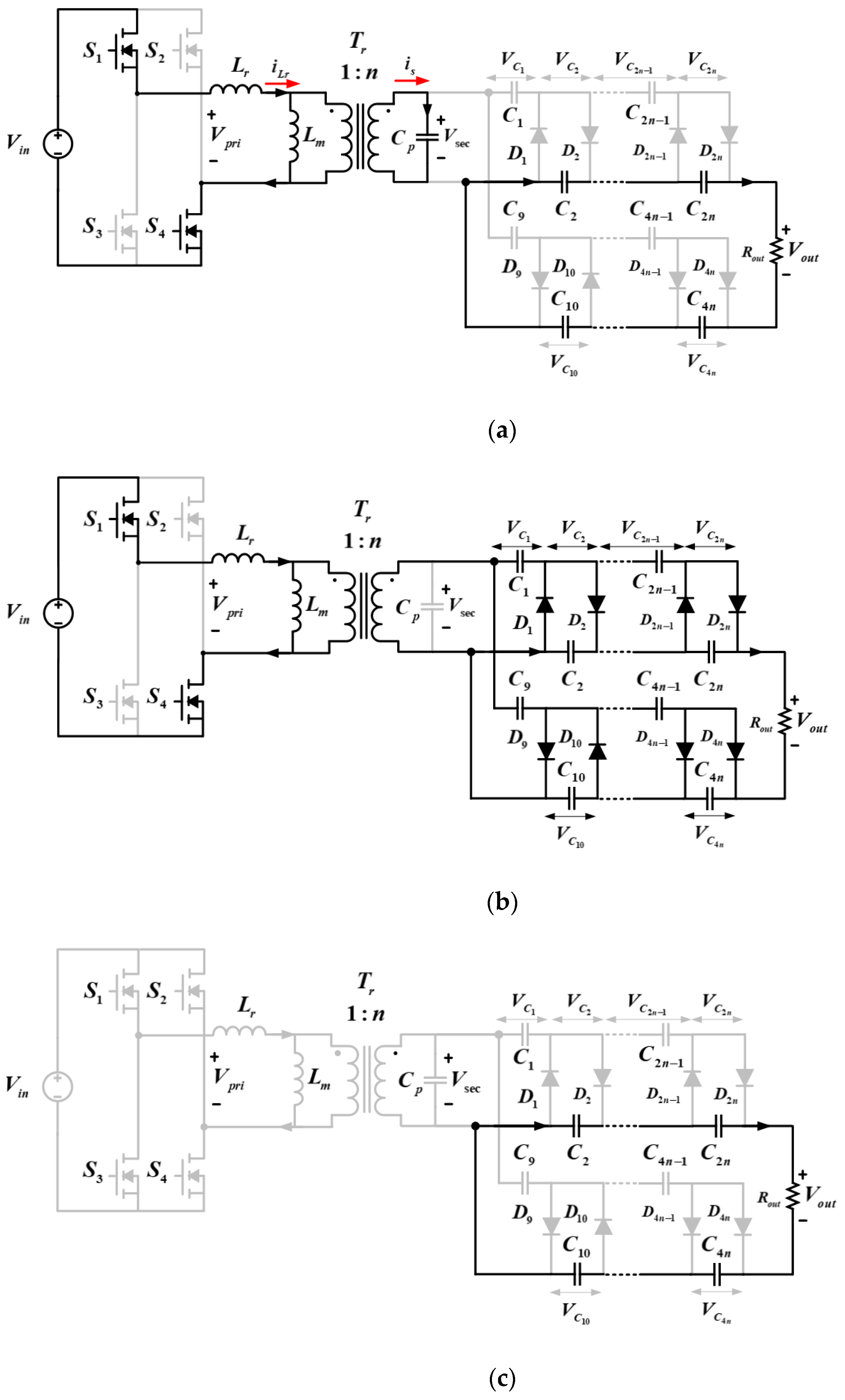
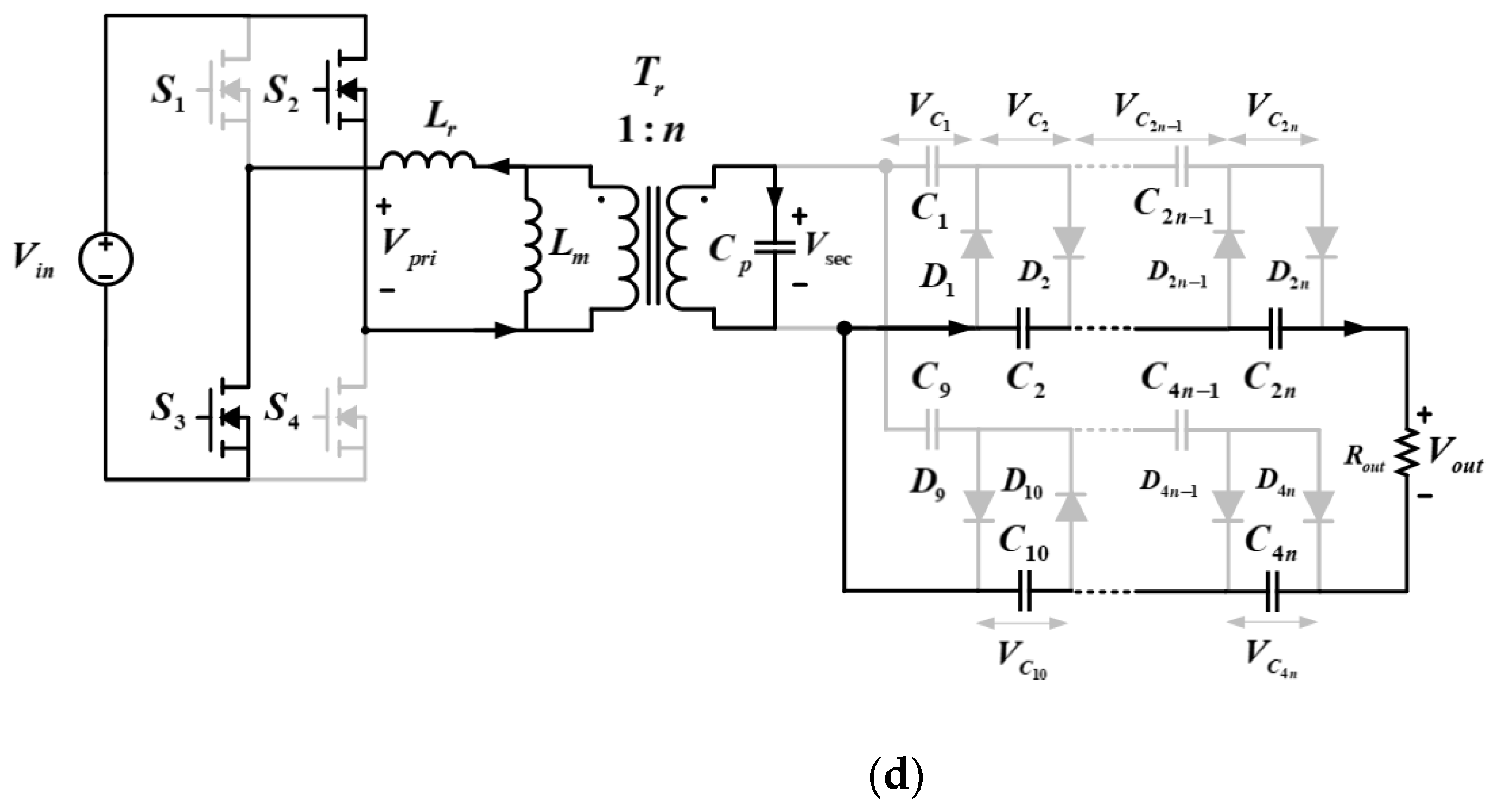
Figure 2 and
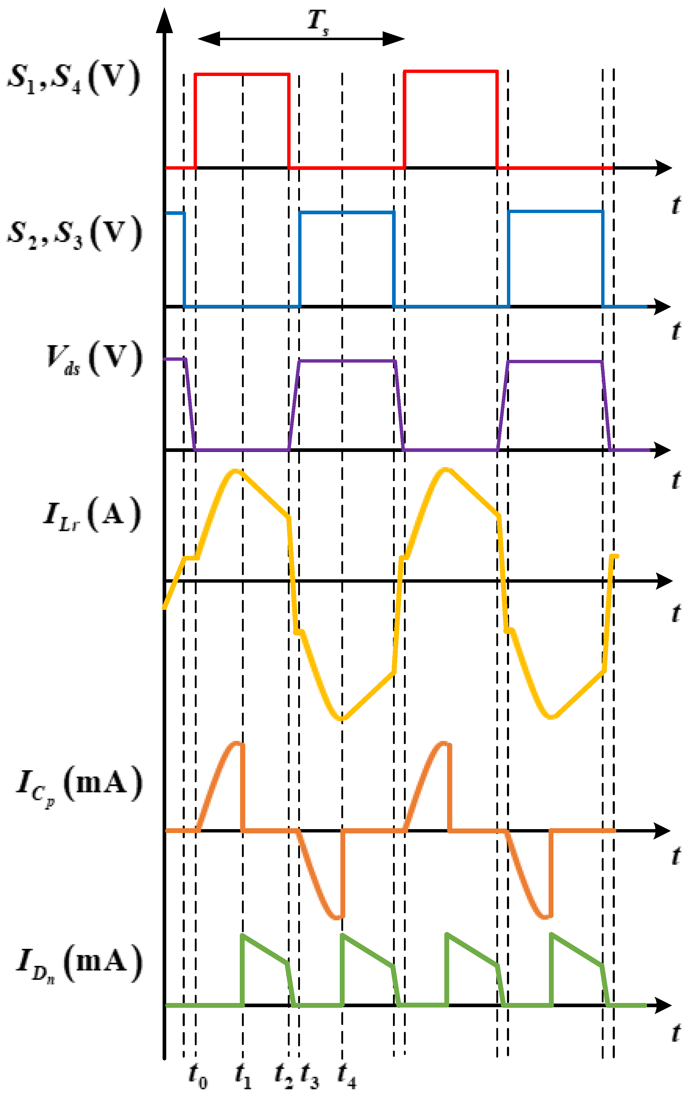
Figure 3 show the operating principle and key waveforms of the proposed parallel resonant converter, respectively. For an analysis of the operation of the converter, the parasitic components generated at the primary side of the transformer and the components generated at the capacitor of the voltage multiplier circuit stage are not considered.
MODE 1 : this mode starts when and are conducting. During this period, the primary side resonant current flows in the positive direction and flows through the transformer to the secondary side parasitic capacitor . In this operation period, because the capacitor voltage at the voltage multiplier circuit is greater than the voltage on the secondary side of the transformer , diode becomes reverse biased so that all currents flowing in the secondary side flow toward the secondary side parasitic capacitor . Consequently, the rectifier diodes at the voltage multiplier circuit do not conduct, and the resonant inductor at the primary side and at the secondary side participate in resonance. In addition, the current path is formed by the voltage charged in the capacitor at the voltage multiplier. This mode ends as soon as the voltage across the secondary side parasitic capacitor becomes greater than the capacitor voltage at the voltage multiplier circuit.
MODE 2
: in mode 2,
and
are still conducting, and this mode starts when
becomes higher than
at the voltage multiplier circuit. At this time, the current flows to diodes
and becomes forward biased, making the diodes at the upper and lower voltage multiplier conduct. Consequently, no current flows to the secondary side
, and the transformer voltage
is clamped at
. In addition, because the output voltage is clamped at
, the primary side magnetizing inductor
connected in parallel assumes a voltage. This results in the resonant inductor
, the secondary-side
, and the primary side magnetizing inductor
not participating in resonance, and the primary side resonant current
being linearly decreased. This mode ends when the switching components
and
are turned OFF.
MODE 3 : this mode represents a dead time period and starts when are turned OFF. Consequently, power is not transferred from the primary side to the secondary side. In addition, do not conduct; thus, and the rectifier diode current decrease significantly. This mode ends when and conduct.
MODE 4 : after the switching half cycle is complete at , a new half cycle starts when and conduct.
3. Analysis of Equivalent Circuit of the Proposed Parallel Resonant Converter
The fundamental harmonic approximation (FHA) is used to analyze the primary and secondary sides of the proposed parallel resonant converter and to obtain the voltage gain [
14]. For the analysis, only the first-order harmonic component of the square wave of the input voltage is considered; thus, it is easy to analyze the proposed parallel resonant converter. In addition, the structure of the proposed parallel resonant converter comprises a parallel voltage multiplier at the secondary side and produces a total output voltage of 100 kV. However, in this study, only one voltage multiplier stage producing a 50 kV output voltage is considered.
Equation (4) considers several harmonic components of the primary side voltage. In Equation (5), the equation used for FHA, only the first-order harmonic component is considered; that is, other harmonic orders are not considered. Thus, Equation (5) is used to calculate the voltage gain of the proposed converter.
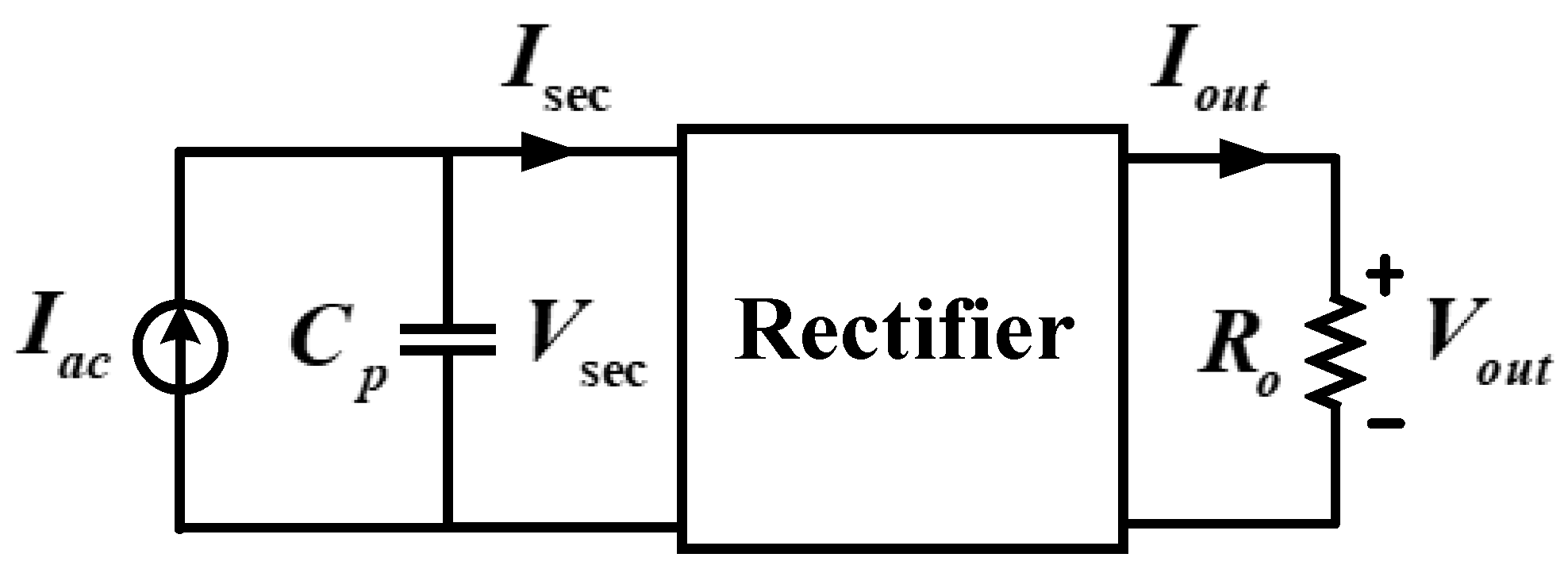
Figure 4 shows the circuit for deriving the equivalent load resistance value. The component on the primary side is replaced by a sinusoidal current source, and the input voltage on the secondary side is expressed as a square wave component. In addition, the average value of the sinusoidal current is the output current, expressed by Equation (6). Equation (7) represents the voltage across the secondary transformer. In the voltage multiplier circuit, this voltage is 1/8 times that of the output voltage. In addition, by dividing Equation (9) by the current component Equation (6), the equivalent load resistance Equation (10) can be obtained.
In high-voltage applications, the secondary side of the transformer has a higher turn ratio than the primary side. If the turn ratio is equalized to the primary side, the equivalent load resistance can be expressed by Equation (11). Therefore, the equivalent resistance equation can be derived, and the voltage gain of the converter can be obtained through the Equations (5) and (9). When the secondary side voltage
is equalized to the primary side, we obtain the voltage gain Equation (12). When the primary side and secondary side voltages are calculated, the voltage gain can be expressed as Equation (13).
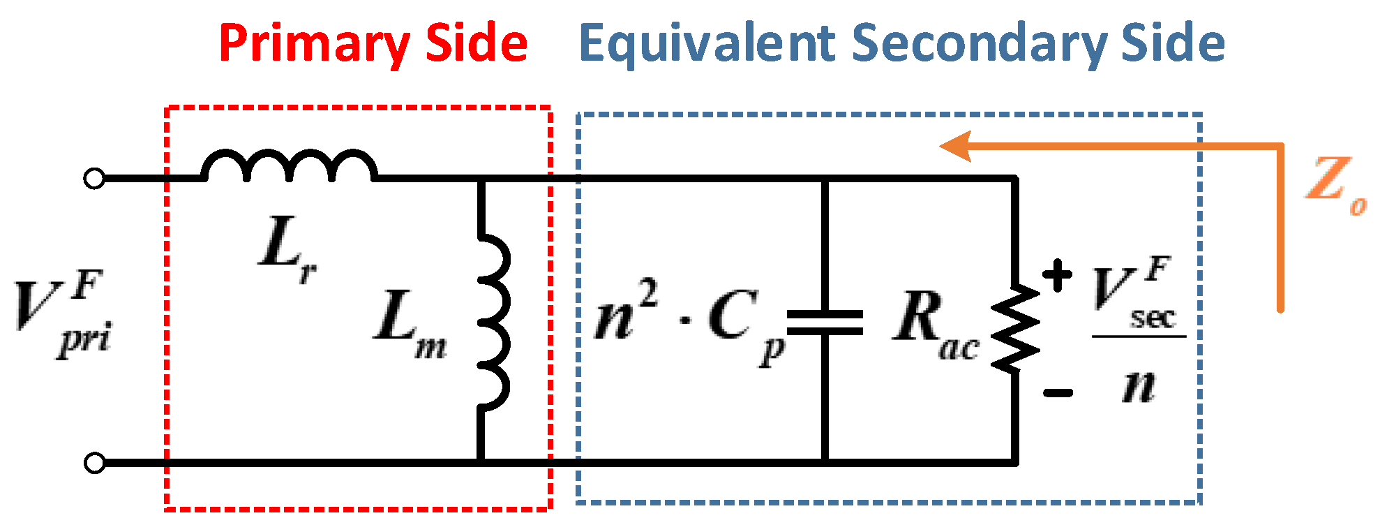
Figure 5 shows the AC equivalent circuit of the proposed parallel resonant converter. In order to derive the necessary equation for the parallel resonant converter, it is necessary to calculate the characteristic impedance
using the resonant inductor
, magnetizing inductance
, equivalent resistance
, and the equivalent resonant capacitance
. These resonance tank components can be expressed as follows.
In the case of a parallel resonant converter, the impedance of the inductor, which can be expressed as , is more dominant at a low frequency, whereas the impedance of the capacitor component, which can be expressed as is more dominant at a high frequency. In addition, the resonant inductance and resonant capacitance are canceled at the resonant frequency, as shown in Equation (16). The resonant inductor and resonant capacitor values of the proposed parallel resonant converter can be derived from Equations (17)–(19).
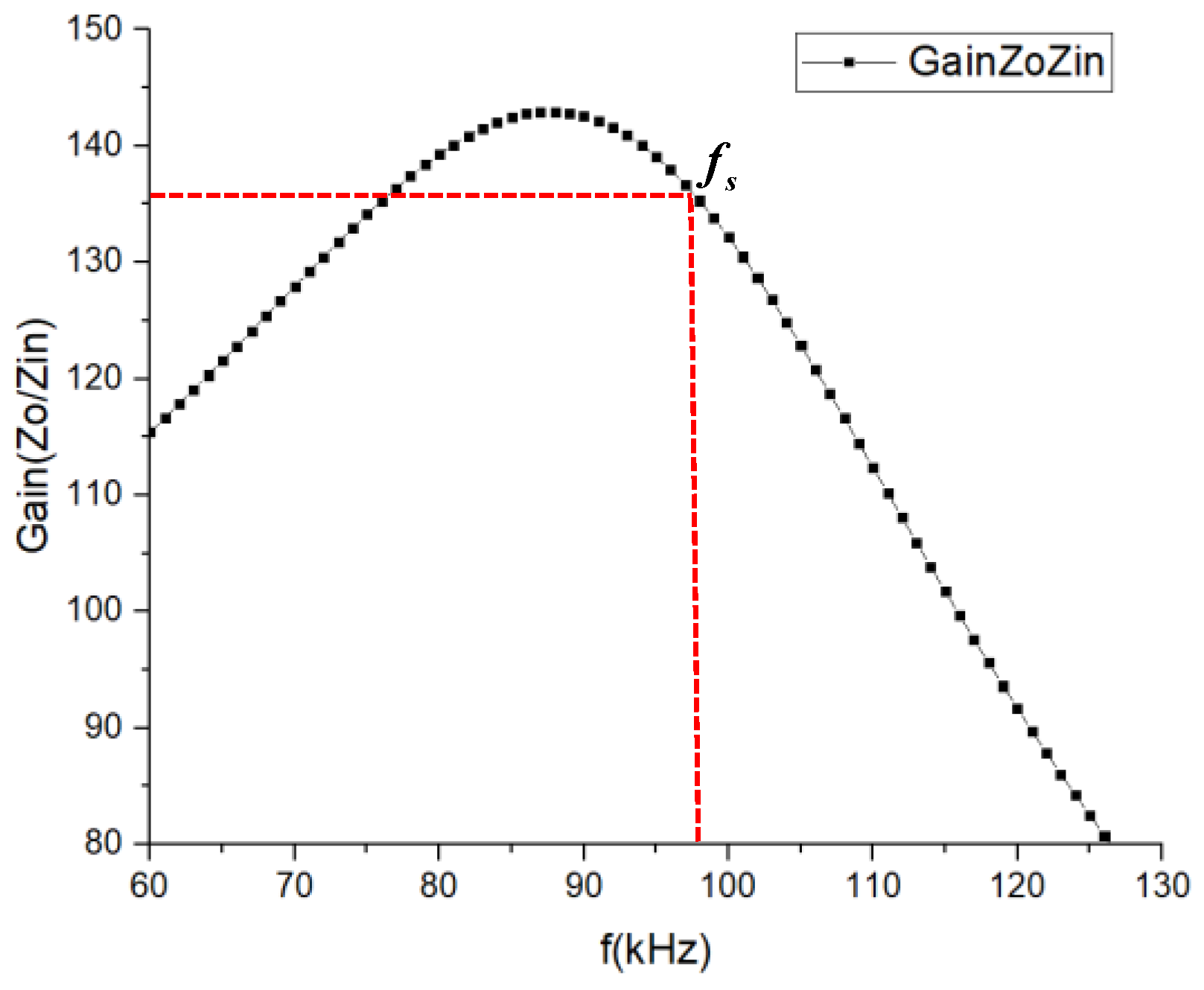
Figure 6 shows the voltage gain curve for an output voltage of 50 kV. This curve is obtained using the equivalent circuit shown in
Figure 5 and the calculated Equations (14) and (17)–(19).
4. Analysis of the Secondary Side Voltage Multiplier
In high-output-voltage applications, a voltage multiplier circuit is used to obtain a much higher output voltage by using a rectifier diode and a capacitor [
15,
16,
17,
18,
19]. For example, in the case of a parallel resonant converter used in high-output-voltage applications such as medical devices, because the output voltage is greater than 5 kV, voltage multiplier circuits are mostly used at the rectifier stage of the converter. Consequently, in this study, four stages and a parallel-structure voltage multiplier are used to obtain an output voltage greater than 100 kV.
The voltage at the secondary side transformer
is required in order to increase the output voltage
. Based on the resonant inductor
on the primary side and the parasitic capacitor
on the secondary side, as shown in
Figure 1, the voltage applied to the secondary side of the transformer
has a pulse waveform with a peak value of 6.25 kV. In addition, this voltage is applied to the capacitor at the voltage multiplier circuit
when the rectifier diode is turned ON. With this principle, the voltage
of 12.5 kV is applied, and
, the current from the four-stage voltage multiplier circuit, is obtained as 50 kV. With this principle, the proposed parallel resonant converter can obtain a final output voltage of 100 kV, with a voltage ranging from −50 kV to 50 kV, using upper and lower voltage multiplier circuits. The pulsed voltage waveforms can be expressed as shown in
Figure 7.
5. Experimental Results
Experiments are conducted to verify the effectiveness of the proposed parallel resonant converter. The operating conditions for the experiment are listed in
Table 1.
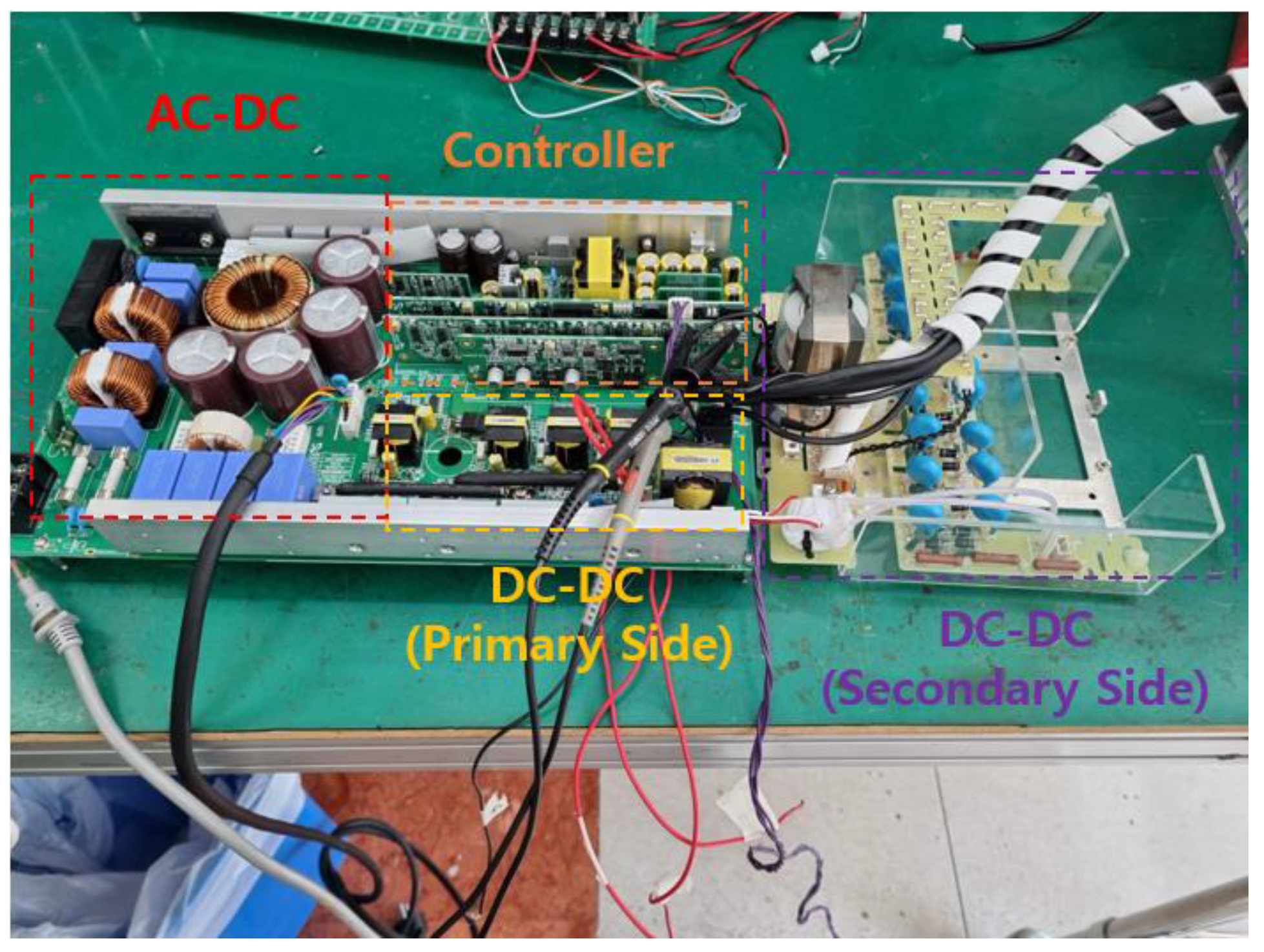
Figure 8 shows the experimental setup of the parallel resonant converter comprising the AC–DC stage, controller, DC–DC primary side, and DC–DC secondary side. It receives an input voltage of 220 V from the AC–DC terminal and converts it to a DC voltage of 380 V, and the converted value, using the transformer and voltage multiplier circuits on the secondary side of the DC–DC converter, finally results in an output voltage of 100 kV, as shown in
Figure 8. In addition, in the experimental setup, the transformer stage and voltage multiplier circuits are separated from the primary side for high-voltage insulation using insulating oil. In addition, a constant current electronic load was applied and operated in a constant current mode.
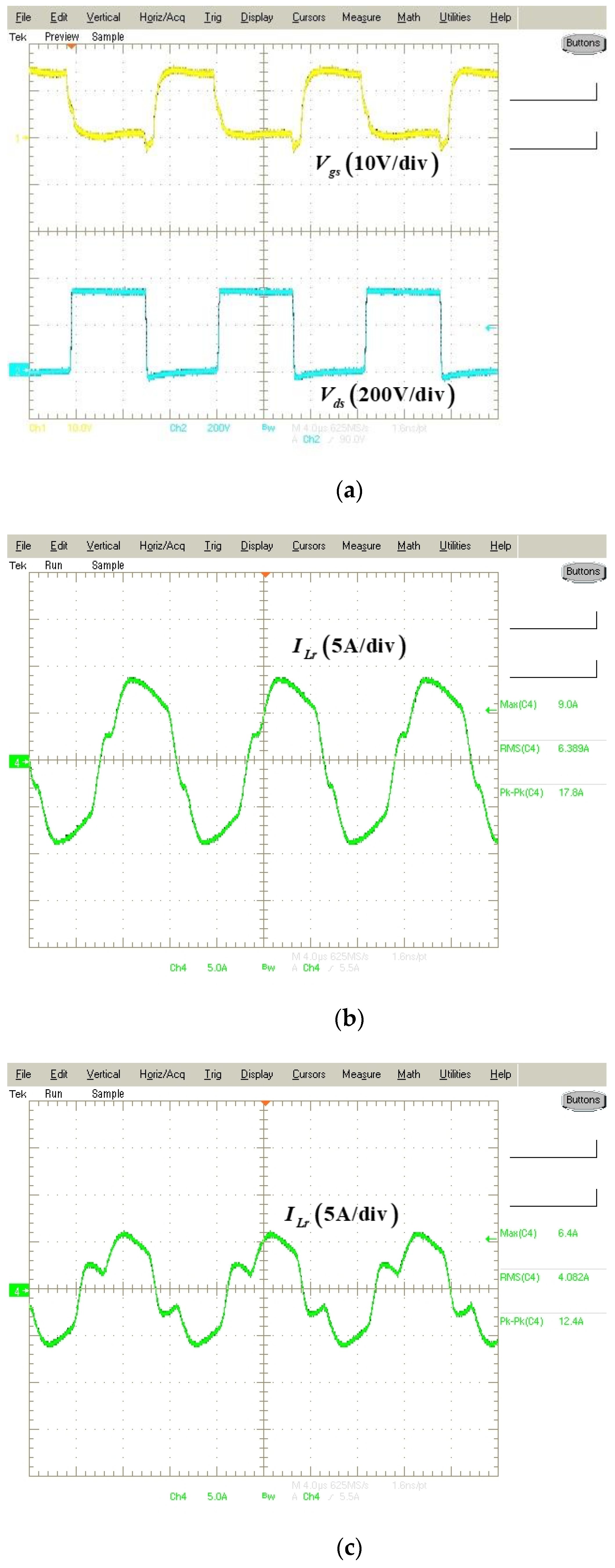
Figure 9 shows the experimental results of the proposed parallel resonant converter.
Figure 9a shows the input gate voltage
of the switching components and voltage
across the switch component. The drain–source voltage is zero because switching components
and
are conducting. In addition, the input voltage
is applied to the voltage
when
and
are not conducting.
Figure 9b shows the primary side resonant inductor current
under the rated load condition. Therefore, the proposed parallel resonant converter has 1.7 kW output power, with an output voltage of 100 kV and an output current of 1.7 mA. In addition, a comparison with the key waveforms analyzed (
Section 2) reveals that the experimental waveforms of the proposed converter are similar to the analyzed waveform, as a resonance between the resonant inductor and the parasitic capacitance occurs in
.
Figure 9c shows the primary side resonant inductor current
at a 50% load. In this case, the current flowing to the secondary side decreases because the output current is less than that of the rated load condition. Under these conditions, the proposed converter operates effectively at a 50% load; however, the primary side resonant current waveform becomes relatively small, owing to the difference in the output current.
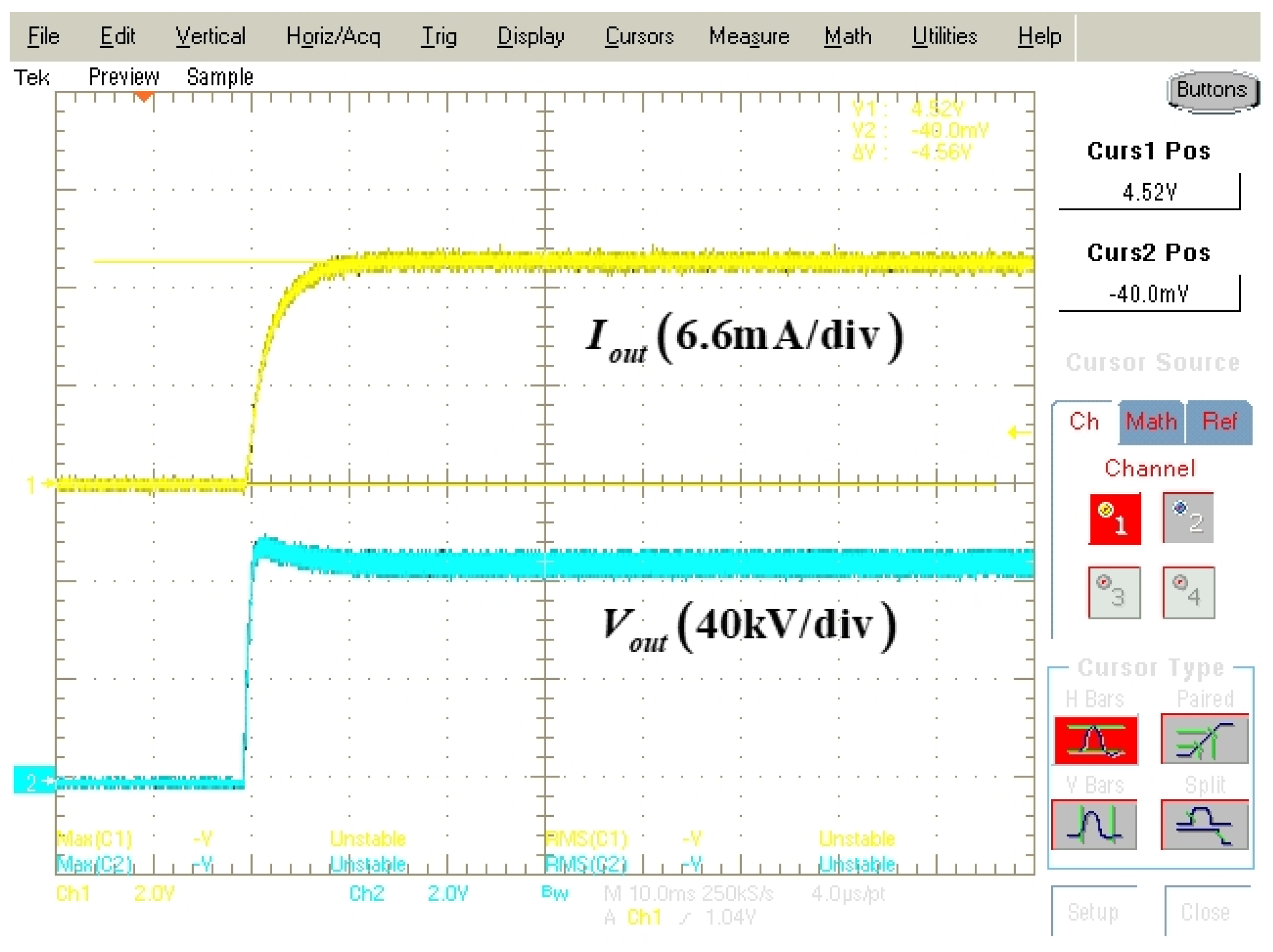
Figure 10 shows the feedback-sensing waveforms of the output voltage and output current at the rated output voltage. Using these voltage waveforms, it is confirmed that the proposed parallel resonant converter has a rated output voltage of 100 kV and an output current of 17 mA. In addition, in high-voltage applications, especially in medical X-rays, because the machines operate for a short time, a constant current load is usually used. Consequently, the sensed output voltage and output current waveforms are different.
6. Conclusions
In this paper, a novel parallel resonant converter structure using parasitic capacitor components on the secondary side of the transformer is proposed. The proposed parallel resonant converter uses the parasitic capacitance of the secondary side transformer instead of using the resonant capacitor on the primary side, which can secure the space on the primary side and so the power density of the parallel resonant converter can be improved. The effectiveness of the proposed structure is confirmed through the analysis of the equivalent model, derivation of new equations, and analysis of the voltage multiplier circuits. In addition, the operation of the proposed parallel resonant converter is verified through an experiment in which the system has an output power, voltage, and current of 1.7 kW, 100 kV, and 1.7 mA, respectively.
Author Contributions
Conceptualization, J.K.; methodology, J.K.; software, J.K.; validation, J.K.; formal analysis, J.K.; investigation, J.K.; writing—original draft preparation, J.K.; writing—review and editing, J.K. and R.-Y.K.; visualization, J.K. and R.-Y.K.; supervision, R.-Y.K. All authors have read and agreed to the published version of the manuscript.
Funding
This research received no external funding.
Conflicts of Interest
The authors declare no conflict of interest.
References
- Ou, Z.; Gao, F.; Zhao, H.; Zhu, L.; Dang, S.; Hu, Y. Design and analysis of LLC resonant converter for X-ray high-voltage power. In Proceedings of the 2019 IEEE 4th Advanced Information Technology-Electronic and Automation Control Conference (IAEAC), Chengdu, China, 20–22 December 2019; pp. 505–510. [Google Scholar]
- Chakraborty, S.S.; Patnala, S.; Bhawal, S.; Hatua, K. Selection procedure of resonant tank parameters for an SiC MOSFET based DC/DC series resonant converter. In Proceedings of the 2018 IEEE International Conference on Power Electronics-Drives and Energy Systems (PEDES), Chennai, India, 18–21 December 2018; pp. 1–5. [Google Scholar]
- Hsu, W.C.; Chen, J.F.; Hsieh, Y.P.; Wu, Y.M. Design and steady-state analysis of parallel resonant DC-DC converter for high-voltage power generator. IEEE Trans. Power Electron. 2017, 312, 957–966. [Google Scholar] [CrossRef]
- Zhang, Z.; Tang, Z. Pulse frequency modulation LLC series resonant X-ray power supply. In Proceedings of the 2011 International Conference on Consumer Electronics-Communications and Networks (CECNet), Xianning, China, 16–18 April 2011; pp. 1532–1535. [Google Scholar]
- Li, F.; Wang, S.; Hou, W.; Qin, X. Design and research on high voltage power supply of medical X-ray machine. In Proceedings of the 2016 IEEE International Conference on Mechatronics and Automation, Harbin, China, 7–10 August 2016; pp. 943–947. [Google Scholar]
- Rąbkowski, J.; Łasica, A.; Zdanowski, M.; Wrona, G.; Starzyński, J. Portable DC Supply Based on SiC Power Devices for High-Voltage Marx Generator. Electronics 2021, 10, 313. [Google Scholar] [CrossRef]
- Liu, Y.; Du, G.; Wang, X.; Lei, Y. Analysis and design of high-efficiency bidirectional GaN-based CLLC resonant converter. Energies 2019, 12, 3859. [Google Scholar] [CrossRef] [Green Version]
- Hu, Y.; Shao, J.; Ong, T.S. 6.6 kW high-frequency full-bridge LLC DC-DC converter with SiC MOSFETs. In Proceedings of the 2019 IEEE Energy Conversion Congress and Exposition (ECCE), Baltimore, MD, USA, 29 September–3 October 2019; pp. 6848–6853. [Google Scholar]
- Jung, J. Bifilar winding of a center-tapped transformer including integrated resonant inductance for LLC resonant converter. IEEE Trans. Power Electron. 2013, 28, 615–620. [Google Scholar] [CrossRef]
- Fei, C.; Lee, F.C.; Li, Q. High-efficiency high power density LLC converter with an integrated planar matrix transformer for high output current applications. IEEE Trans. Power Electron. 2016, 64, 9072–9082. [Google Scholar] [CrossRef]
- Wang, Y.F.; Chen, B.; Hou, Y.; Meng, Z.; Yang, Y. Analysis and design of a 1-MHz bidirectional multi-CLLC resonant DC-DC converter with GaN devices. IEEE Trans. Power Electron. 2020, 67, 1425–1434. [Google Scholar] [CrossRef]
- Liu, J.; Sheng, L.; Shi, J.; Zhang, Z.; He, X. Design of high voltage, high power and high frequency transformer in LCC resonant converter. In Proceedings of the 2009 24th Annual IEEE Applied Power Electronics Conference and Exposition, Washington, DC, USA, 15–19 February 2009; pp. 1034–1038. [Google Scholar]
- Liu, J.; Sheng, L.; Shi, J.; Zhang, Z.; He, X. LCC resonant and converter operating under discontinuous resonant current mode in high voltage, high power, and high-frequency applications. In Proceedings of the 2009 24th Annual IEEE Applied Power Electronics Conference and Exposition, Washington, DC, USA, 15–19 February 2009; pp. 1482–1486. [Google Scholar]
- Ericson, R.; Maksimovic, D. Fundamentals of Power Electronics, 2nd ed.; University of Colorado: Boulder, CO, USA, 2001; pp. 715–722. [Google Scholar]
- Leu, C.; Huang, P. A novel voltage doubler rectifier for high output voltage applications. In Proceedings of the 2010 International Power Electronics Conference (ECCE), Sapporo, Japan, 21–24 June 2010; pp. 2082–2085. [Google Scholar]
- Mao, S.; Popovic, J.; Ferreira, J. High voltage pulse speed study for high voltage DC-DC power supply based on voltage multipliers. In Proceedings of the 2015 17th European Conference on Power Electronics and Applications, Geneva, Switzerland, 8–10 September 2015; pp. 1–10. [Google Scholar]
- Katzir, L.; Shmilovitz, D. A high voltage split source voltage multiplier with increased output voltage. In Proceedings of the 2015 IEEE Applied Power Electronics Conference and Exposition (APEC), Charlotte, NC, USA, 15–19 March 2015; pp. 3272–3275. [Google Scholar]
- Lin, B.-R.; Lin, G.-H.; Jian, A. Resonant Converter with Voltage-Doubler Rectifier or Full-Bridge Rectifier for Wide-Output Voltage and High-Power Applications. Electronics 2019, 8, 3. [Google Scholar] [CrossRef] [Green Version]
- Uno, M.; Nakane, T.; Shinohara, T. LLC Resonant Voltage Multiplier-Based Differential Power Processing Converter Using Voltage Divider with Reduced Voltage Stress for Series-Connected Photovoltaic Panels under Partial Shading. Electronics 2019, 8, 1193. [Google Scholar] [CrossRef] [Green Version]
| Publisher’s Note: MDPI stays neutral with regard to jurisdictional claims in published maps and institutional affiliations. |
© 2021 by the authors. Licensee MDPI, Basel, Switzerland. This article is an open access article distributed under the terms and conditions of the Creative Commons Attribution (CC BY) license (https://creativecommons.org/licenses/by/4.0/).

