1. Introduction
Fault diagnosis is an important element in the design and test of integrated circuits. Especially with the development of CMOS circuits, it is more and more difficult to detect faults only with limited input and output ports. BIST is a viable approach that has been used by many researchers [
1,
2,
3,
4,
5,
6,
7,
8,
9].
For data converter fault diagnosis schemes, there are schemes based on Differential Non-Linearity (DNL) test data [
1], based on code-width [
2], based on a resistance matching [
3], and so on. For amplifier fault diagnosis schemes, there is a scheme by using an RF peak detector and two comparators [
4], a scheme by checking the stable output of transient response [
5], a scheme based on chaotic oscillation [
6], and so on. For sample and hold circuit fault diagnosis schemes, there is a scheme by online balance self-checking [
7], a scheme by measuring performance parameters [
8], a scheme by monitoring the same output with common-mode input [
9], and so on.
Bootstrapped switches are widely used in many mixed-signal circuits [
10,
11,
12,
13]. For example, they are used in sample and hold circuits to achieve rail-to-rail switching functions [
10,
11], used in charge pump circuits to improve energy harvesting by node pre-charging [
12,
13], and so on. There are also reports on improving the performance of bootstrap switches [
14,
15,
16]. For example, the body effect compensation technology is used to improve the linearity of the bootstrapped switch [
14,
15], the dual-channel sampling switch technology is used to improve the accuracy and linearity of the bootstrapped switch [
16], and so on. However, there are few reports on the fault diagnosis schemes for bootstrapped switches.
Consequently, this paper proposes a BIST scheme for detecting catastrophic faults in bootstrapped switches.
Section 2 previews the bootstrapped switch under testing.
Section 3 presents the model of fault diagnosis.
Section 4 presents the BIST implementation.
Section 5 sets the simulation result by HSPICE.
Section 6 discusses the results.
Section 7 sets the conclusion.
2. The Bootstrapped Switch under Test
In this study, the bootstrapped switch in [
17] was used as the circuit under test. The circuit and the designed size of elements are shown in
Figure 1.
CLK is the clock signal, which controls the “ON” phase and “OFF” phase of the bootstrapped switch.
Vin is the input signal.
Vout is the output signal.
VG is the gate voltage of the sampling MOS transistor.
When the bootstrapped switch is in the “ON” phase, the CLK is “1”. Then, the voltage of Node 4 is pulled down to GND via M7 and the voltage of Node 2 is pulled down to GND via M10. Then, the voltage of Node 3 is pulled up to VDD via M9, the voltage of Node 5 follows the voltage of Vin via M6 and the voltage of Node 8 follows the voltage of Node 6 via M3. The voltage of Node 5 is transmitted to Node 6 via C2, so the voltage of Node 6 is the voltage of Vin plus the voltage previously-stored at node 6.
When the bootstrapped switch is in the “OFF” phase, the CLK is “0”. Then, the voltage of Node 2 is pulled up to VDD via M11 and the voltage of Node 4 follows the voltage of Node 3 via M8. Then, the voltage of Node 3 is pulled up to 2VDD via C1, so the voltage of Node 4 is 2VDD. Then, the voltage of Node 8 is pulled down to GND via M2 and M1. Then, the voltage of Node 6 follows the voltage of Node 4 via M4.
So, the voltage of Node 6 is 2VDD in the “OFF” phase and 2VDD plus the voltage of Vin in the “ON” phase.
The Bootstrapped technique improves linearity by increasing the voltage at the node to lower and stabilize the on-resistance of the sampling switch. In this study, the transmission voltage reached 2VDD, which was difficult to set up the test circuit.
3. The Proposed BIST Scheme
When the bootstrapped switch is in the “ON” phase, the gate voltage of the sampling MOS transistor has a stable voltage. When the bootstrapped switch in the “OFF” phase, the gate voltage of the sampling MOS transistor is GND. According to this characteristic, the gate voltage of sampling MOS transistor and CLK signal are used as observation signals.
Due to the bootstrapped switch in this study, in the “ON” phase, the gate voltage of the sampling MOS transistor is 2VDD. If the power supply voltage is 1.8 V, then the gate voltage of the sample MOS transistor is 3.6 V. Such a high voltage is not suitable for observation.
To solve this problem, a low power supply voltage is provided to the bootstrapped switch. As a result, an appropriate voltage can be obtained on the sampling MOS transistor during the “ON” phase.
The testing strategy is if the response analysis module meets the following conditions, output “F = 0”, it indicates that the circuit is fault-free; otherwise output “F = 1”, indicates that the circuit has faults.
1. When “CLK = 1”, the gate voltage of the sampling MOS is a constant value. In this study, the value is determined by a window comparator.
2. When “CLK = 0”, the gate voltage of the sample MOS is GND. In this study, the GND is determined by a phase inverter.
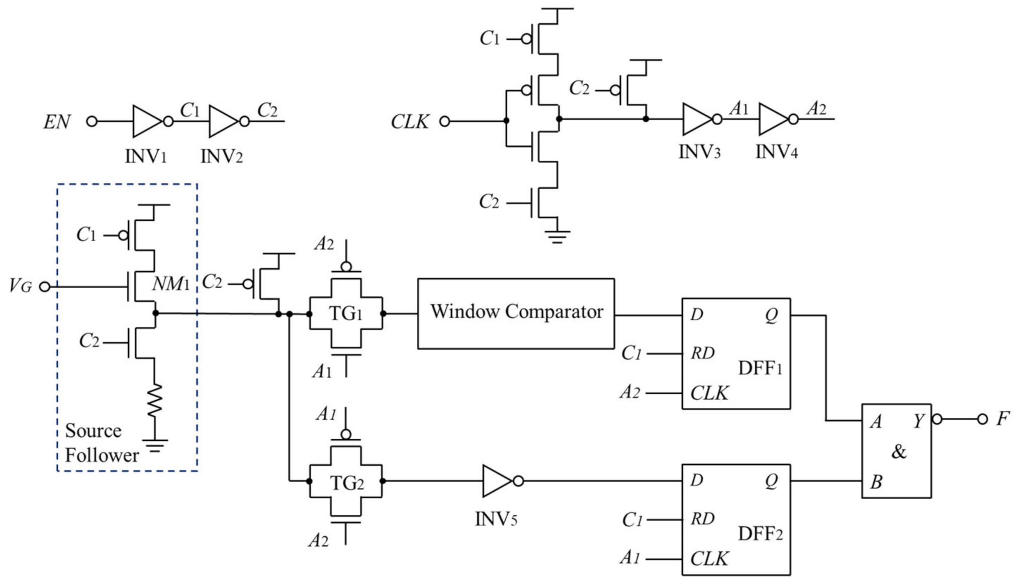
The proposed BIST schematic is shown in
Figure 2. The
CLK signal of the bootstrapped switch and the gate voltage of the sampling MOS (
VG) are connected to the response analysis module as the input. The response analysis module analyzes the two-observation signal to determine whether the circuit has a fault. The
EN is an enabling signal that controls whether the analysis module works. The power supply voltage of the bootstrapped switch is
VDD1. The power supply voltage of the response analysis is
VDD2.
The schematic of the response analysis module is shown in
Figure 3. When “
EN =
0”, the response analysis module is not working. The
CLK signal and
VG signal do not affect the response analysis module. The output
F is “1”. When “
EN =
1”, the analysis module works. If the output is “
1”, it indicates that the circuit is fault-free. If the output is “
0”, it indicates that the circuit has faults. Because the bootstrapped switch is sensitive to the changes of
VG signal, a source follower is used to collect the
VG signal.
The schematic of the window comparator in [
5] is shown in
Figure 4. The window comparator outputs a high potential within the designed input range. The input range can be adjusted by adjusting the W/L of the four inverters.
4. Fault Modeling
To evaluate the proposed test strategy, six fault models were added to the circuit under testing. The fault models considered in this paper are shown in
Figure 5.
The short fault of MOS transistor is simulated by a 10Ω resistor between two ports connected. The specific ones are
Figure 5a gate-drain short (GDS),
Figure 5b gate-source short (GSS), and
Figure 5c drain-source short (DSS), respectively. The open fault of MOS transistor is simulated by inserting a 100
fF capacitor and a 10 MΩ resistor in parallel at the port. The specific ones are
Figure 5d drain open (DO),
Figure 5e source open (SO), and
Figure 5f gate open (GO), respectively.
5. Simulation Results
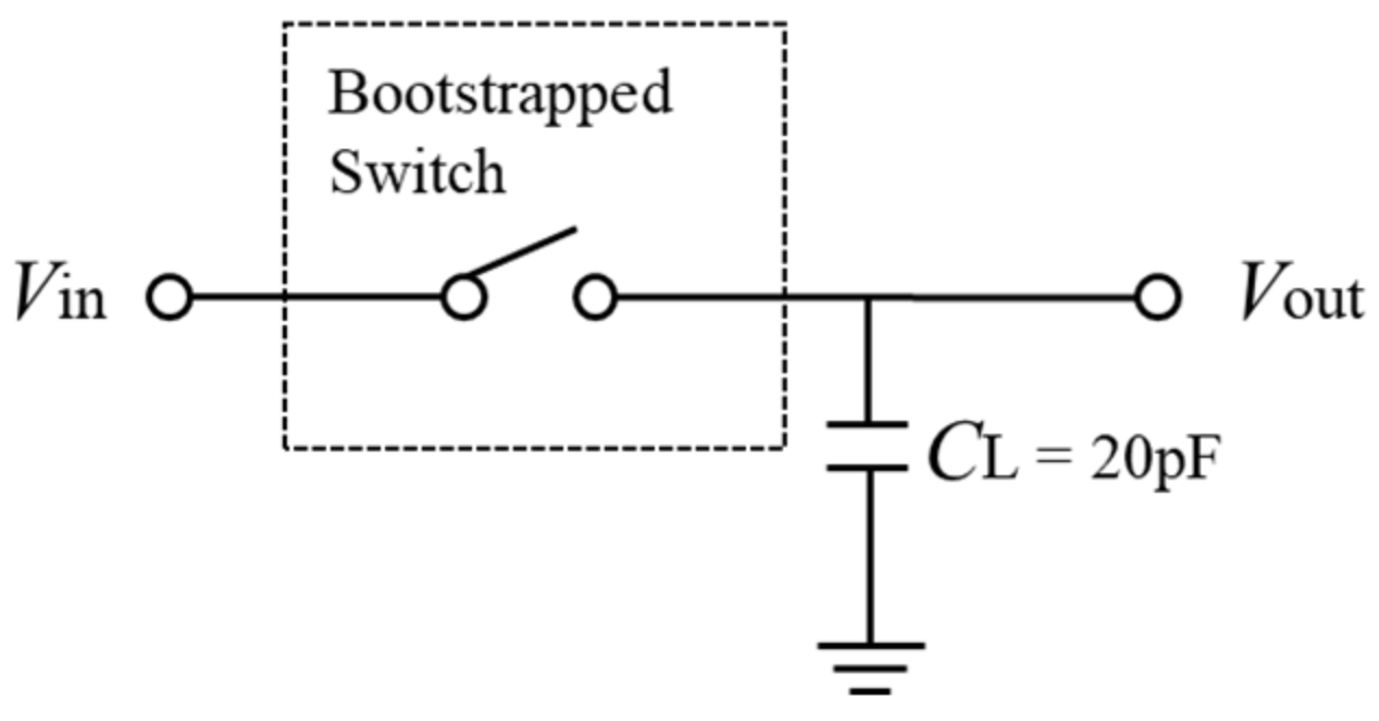
To obtain the influence information of BIST on the bootstrapped switch, the performance simulation of the bootstrapped switch with and without the test circuit was carried out. As shown in
Figure 6, the bootstrapped switch and a 20 pF capacitor are combined into a track and hold circuit. The CUT schematic is shown in
Figure 1. The schematic of CUT with BIST is shown in
Figure 2.
The
CLK signal is a 10 M Hz square wave and the input signal is a sine wave with an amplitude of 1.8 V and a frequency of 4.96 M Hz. After the spectrum analysis of the circuit, the performance parameters in
Table 1 were obtained. The simulation results show that the BIST scheme has no obvious burden on the CUT. Note a slight decrease in SNR, which is due to the additional noise provided by
NM1. The
VGS of the
MS with BIST scheme is higher than that of the
MS without the BIST scheme, which results in the on-resistance of the
MS with the BIST scheme being lower than that of the
MS without the BIST scheme. Therefore, the parameters except SNR are slightly improved.
To evaluate the proposed BIST scheme, a fault attachment script was used to add the six faults to the MOS transistor of the bootstrapped switch except for the MS. The fault of DSS, DO and SO of MS does not cause voltage changes at the gate voltage of MS which as observation voltage. Therefore, this BIST scheme cannot detect the fault of DSS, DO and SO of MS. However, the MS connects the input and output signals, a fault in the MS can be easily detected by other methods. Therefore, the MS is not used as a test object. The total number of fault circuits is 66.
The VDD1 and the input signal are set to 0.6 V, thus the VG is approximately 1.56 V during the “ON” phase. Therefore, the output voltage of the source follower is carefully designed to be approximately 0.7 V, when the input voltage of the source follower is approximately 1.56 V. To cope with the possible deviation of the circuit manufacturing, the window voltage of the window comparator is designed to be 0.5 V to 0.9 V.
Figure 7 shows the output signal by transient simulation.
Figure 7a shows the result of fault-free. When BIST is off, the output is “
F =
1”; when BIST is on, the output is “
F =
0” which indicates that the circuit is fault-free.
Figure 7b shows the result of a fault with gate-source short with the
M1. When BIST is off, the output is “
F =
1”; when BIST is on, the output is “
F =
1” which indicates that the circuit has faults.
Table 2 shows the simulation results with 66 test circuits. The fault coverage of the BIST scheme is approximately 87.9%. The 200 times Monte-Carlo simulation results show that the BIST scheme works well. Extreme process simulation results show that the fault coverage of the BIST scheme is approximately 75.8%, 78.8%, 89.4% and 84.8% at FF, FS, SS and SF corner, respectively.
6. Discuss
The function of M2 is to relieve the pressure of M1, that is, to prevent the drain-source voltage of M1 from being greater than VDD. M2 can be equivalent to resistance. Therefore, the BIST scheme cannot be detected to the fault of DSS of M2.
Note that the BIST scheme has low fault coverage for the gate open of the MOS transistor. This issue is discussed with the fault of GO of M1.
Figure 8 shows the transient simulation of the gate voltage of
M1 with the fault of GO with
M1. Although the gate of
M1 is open, the gate voltage of
M1 is still high and low at the right time sequence due to the presence of parasitic capacitance. Therefore,
M1 can be turned on and off at the correct timing with the gate open. This indicates that the effect of this type of fault on the circuit is not catastrophic. However, this fault may still affect the circuit performance, and subsequent research will be carried out to address this issue.
7. Conclusions
Bootstrapped switches are an indispensable type in analog circuits, but there are few fault diagnosis schemes for them. Thus, this paper proposed a bootstrapped switch BIST scheme for detecting catastrophic faults. According to the characteristics of the bootstrap switch, the clock signal and the gate voltage of the sampling MOS transistor are used as the observation signals. However, the gate voltage of the sampling MOS transistor reaches 2VDD during sampling, which is not conducive to observation. In this paper, the method of low power supply voltage is adopted to solve this problem. The proposed BIST scheme was designed and simulated in 0.18 μm CMOS technology. The HSPICE simulation results show that the fault coverage is approximately 87.9% with 66 test circuits. However, in the real circuit, the test result of this BIST scheme may be lower than the simulation results due to noise, technology, or any uncertainty. Therefore, we plan to test and evaluate the prototype chip after it is delivered in the future.
Author Contributions
Conceptualization, X.-B.T. and M.T.; methodology, X.-B.T.; validation, M.T.; resources, M.T.; writing—original draft preparation, X.-B.T.; writing—review and editing, X.-B.T. and M.T.; visualization, X.-B.T.; supervision, M.T.; project administration, M.T.; funding acquisition, M.T. Both authors have read and agreed to the published version of the manuscript.
Funding
This research was funded by JSPS KAKENHI, grant number JP21K11813.
Acknowledgments
This work was supported by VLSI Design and Education Center (VDEC), the University of Tokyo in collaboration with Synopsys, Cadence Design System, Mentor Graphics, Rohm Corporation and Toppan Printing Corporation.
Conflicts of Interest
The authors declare no conflict of interest.
References
- Charoenrook, A.; Soma, M. Fault diagnosis of flash ADC using DNL test. In Proceedings of the IEEE International Test Conference-(ITC), Baltimore, MD, USA, 17–21 October 1993; pp. 680–689. [Google Scholar]
- Lee, D.; Yoo, K.; Kim, K.; Han, G.; Kang, S. Code-width testing-based compact ADC BIST circuit. IEEE Trans. Circuits Syst. II Express Briefs 2004, 51, 603–606. [Google Scholar] [CrossRef]
- Yuan, J.; Tachibana, M. A resistance matching based self-testable current-mode R-2R digital-to-analog converter. IEICE Electron. Express 2013, 10, 1–7. [Google Scholar] [CrossRef] [Green Version]
- Ayadi, R.; Masmoudi, M. A new built-in self-test (BIST) for a RF low-noise amplifier (LNA). In Proceedings of the 5th International Conference on Design & Technology of Integrated Systems in Nanoscale Era, Al Hammamat, Tunisia, 23–25 March 2010; pp. 1–5. [Google Scholar]
- Yuan, J.; Tachibana, M. A BIST scheme for operational amplifier by checking the stable output of transient response. In Proceedings of the 20th European Conference on Circuit Theory and Design (ECCTD), Linkoping, Sweden, 29–31 August 2011; pp. 885–888. [Google Scholar]
- Wannaboon, C.; Nattagit, J.; Tachibana, M. Chaotic oscillation-based BIST for CMOS operational amplifier. In Proceedings of the 2014 International SoC Design Conference (ISOCC), Jeju, Korea, 3–6 November 2014; pp. 30–131. [Google Scholar]
- Kolarik, V.; Lubaszewski, M.; Courtois, B. Towards self-checking mixed-signal integrated circuits. In Proceedings of the ESSCIRC’93: Nineteenth European Solid-State Circuits Conference, Sevilla, Spain, 22–24 September 1993; pp. 202–205. [Google Scholar]
- Axelos, N.; Watson, J.; Taylor, D.; Platts, A. Built-in-self-test of analogue circuits using optimised fault sets and transient response testing. In Proceedings of the Eighth IEEE International On-Line Testing Workshop (IOLTW 2002), Isle of Bendor, France, 8–10 July 2002; pp. 135–139. [Google Scholar]
- Yuan, J.; Tachibana, M. A common-mode BIST technique for fully-differential sample-and-hold circuits. IEICE Electron. Express 2012, 9, 1128–1134. [Google Scholar] [CrossRef] [Green Version]
- Fayomi, C.J.B.; Roberts, G.W.; Sawan, M. Low-voltage CMOS analog bootstrapped switch for sample-and-hold circuit: Design and chip characterization. In Proceedings of the 2005 IEEE International Symposium on Circuits and Systems, Kobe, Japan, 23–26 May 2005; pp. 2200–2203. [Google Scholar]
- Pouya, P.; Ghasemi, A.; Aminzadeh, H. A low-voltage high-speed high-linearity MOSFET-only analog bootstrapped switch for sample-and-hold circuits. In Proceedings of the 2015 2nd International Conference on Knowledge-based engineering and Innovation (KBEI), Tehran, Iran, 5–6 November 2015; pp. 418–421. [Google Scholar]
- Ballo, A.; Grasso, A.D.; Palumbo, G. Charge pump improvement for energy harvesting applications by node pre-charging. IEEE Trans. Circuits Syst. II Express Briefs 2020, 67, 3312–3316. [Google Scholar] [CrossRef]
- Ballo, A.; Palumbo, G.; Grasso, A.D. A Review of Power Management Integrated Circuits for Ultrasound-Based Energy Harvesting in Implantable Medical Devices. Appl. Sci. 2021, 11, 2487. [Google Scholar] [CrossRef]
- Dong, S.; Liu, M.; Zhu, Z.; Yang, Y. A high linear CMOS body effect compensation bootstrapped switch. J. Circuits Syst. Comput. 2015, 24, 1550032. [Google Scholar] [CrossRef]
- Ballo, A.; Grasso, A.D.; Palumbo, G. Current-mode body-biased switch to increase performance of linear charge pumps. Int. J. Circuit Theory Appl. 2020, 48, 1864–1872. [Google Scholar] [CrossRef]
- Wang, L.; Yin, W.J.; Xu, J. Dual-channel bootstrapped switch for high-speed high-resolution sampling. Electron. Lett. 2006, 42, 1275–1276. [Google Scholar] [CrossRef]
- Rabuske, T.; Fernandes, J. A sar adc with a moscap-dac. IEEE J. Solid-State Circuits 2016, 51, 1410–1422. [Google Scholar] [CrossRef]
| Publisher’s Note: MDPI stays neutral with regard to jurisdictional claims in published maps and institutional affiliations. |
© 2021 by the authors. Licensee MDPI, Basel, Switzerland. This article is an open access article distributed under the terms and conditions of the Creative Commons Attribution (CC BY) license (https://creativecommons.org/licenses/by/4.0/).


