Article

Analysis and Design of a Microphone Preamplifier for Mobile Applications

Department of Electronic Engineering, Hanyang University, Seoul 04763, Korea
*
Author to whom correspondence should be addressed.
Electronics 2021, 10(14), 1624; https://doi.org/10.3390/electronics10141624
Submission received: 28 May 2021 / Revised: 4 July 2021 / Accepted: 5 July 2021 / Published: 7 July 2021
(This article belongs to the Section Circuit and Signal Processing)

Abstract

:
A design of an on-chip ac-coupling preamplifier for mobile applications is presented. A microphone preamplifier should have a large input impedance to mitigate the effective-gain reduction caused by the microphone’s non-zero output impedance. From a review of previously reported microphone preamplifier structures in terms of input impedance, feasibility of on-chip ac-coupling, and noise performance, we chose an inverting amplifier structure with capacitive feedback. In addition, to provide dc bias path, we used off-state MOSFET switches as pseudo-resistors of very large resistance in the giga-ohm range. The large resistance enables on-chip ac-coupling with sufficient noise performance. A fast start-up is achieved by turning-on the switch for a short period during the preamplifier start-up. The gain of the preamplifier can be programmed from 0 dB to 21 dB with 3 dB steps. A 2-stage pseudo-class-AB amplifier was adopted to reduce power consumption. The proposed preamplifier was implemented using a 28 nm CMOS process and achieves 107 dB dynamic range in a 20 kHz bandwidth under 0 dB gain setting and balanced differential input signal. The preamplifier dissipates a power of 270 μW with a 1.8 V supply.

1. Introduction

Recent advances of mobile audio devices such as true wireless stereos and cellular phones require microphone read-out integrated circuits (M-ROICs) with wide dynamic range (DR). Furthermore, the power consumption of the M-ROIC should be kept low to make the battery life acceptably long. Besides electrical performance, the silicon area occupied by the M-ROIC and the area occupied on the printed circuit board (PCB) by the silicon chip and auxiliary passive devices such as ac-coupling capacitors becomes more critical for the mobile applications, because the number of the required audio recording channels is increasing to enhance the audio quality by techniques such as echo cancellation and environmental noise cancellation [1,2].
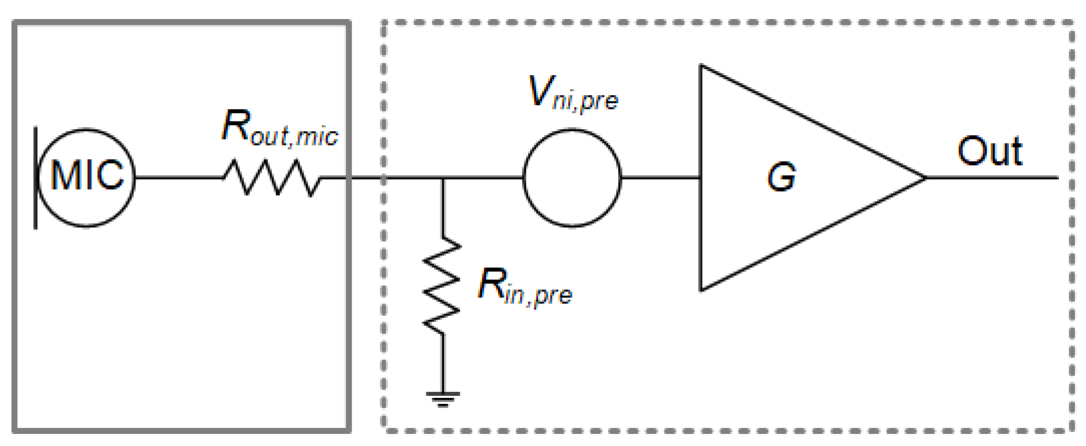
A microphone is a small sensor device that produces electrical signals from sound pressure. The electrical signals should be converted into digital signals by an audio ADC for the desired digital signal processing. However, the small amplitude of the microphone’s output signals, and the uncertain dc level of the output make it unpractical for a microphone to drive ADCs directly. Therefore, a preamplifier is usually used in an M-ROIC to handle such obstacle [3,4,5,6,7,8].
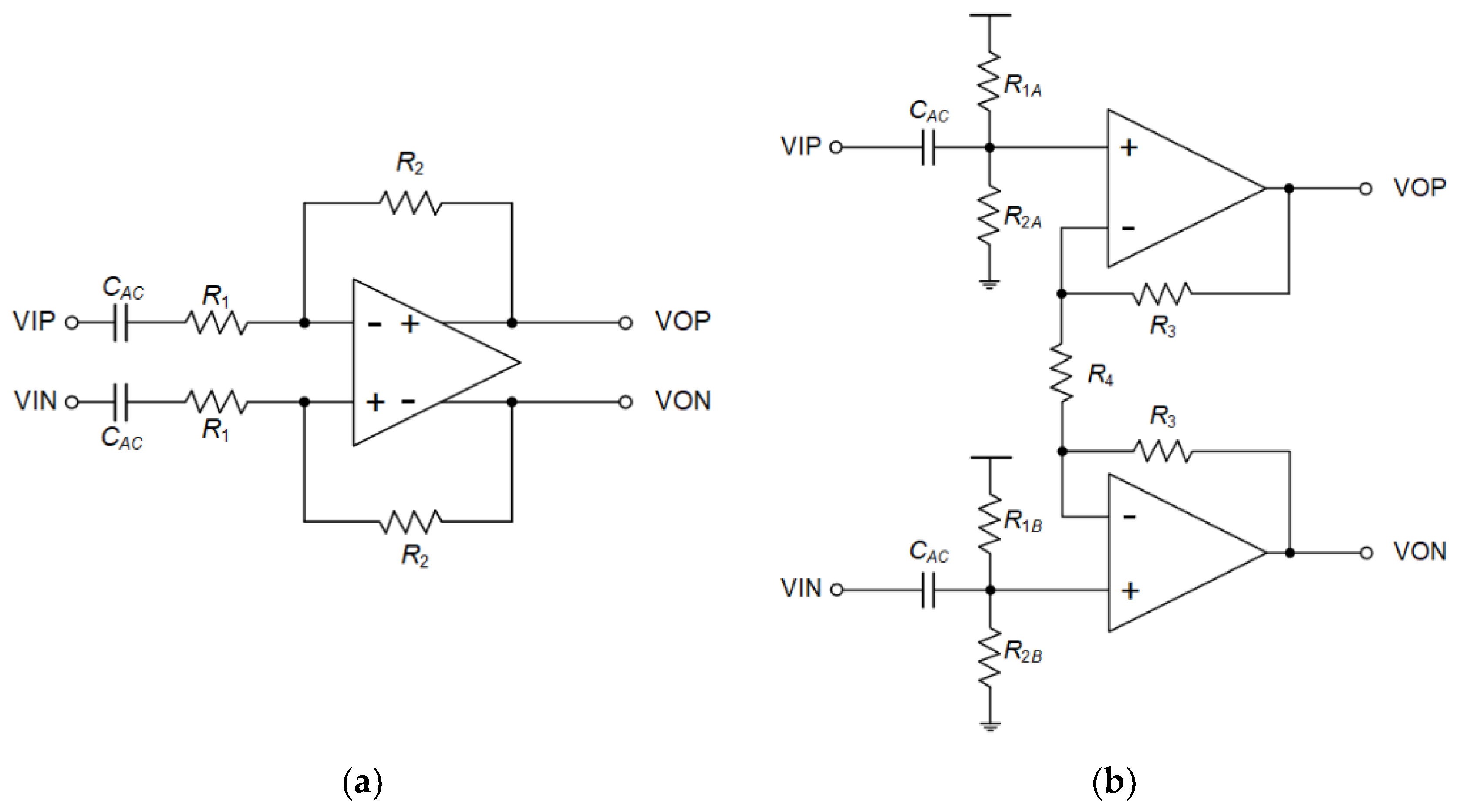
Microphones have non-zero output resistance, which is usually in the kilo-ohms range. This dictates that the preamplifier should have a large input impedance to avoid the reduction of the effective gain. There are a variety of preamplifier structures that aim for different performances, and each of them has different drawbacks. For example, inverting an amplifier with resistive feedback can achieve over 100 dB dynamic range (DR). However, the required noise level for the SNR limits the input impedance of the preamplifier, which leads to effective gain reduction [3,4,5,6]. Moreover, typical resistive feedback architectures require large off-chip ac-coupling capacitors to obtain a lower cut-off frequency of less than 20 Hz, which is undesirable in mobile applications requiring a very small footprint.
This paper presents a high performance programmable-gain microphone preamplifier with on-chip ac-coupling capacitors for driving an audio ADC. The preamplifier adopts an inverting architecture with capacitive feedback because of its large input impedance. Pseudo-resistors with very large resistance were employed to realize ac-coupling with on-chip capacitors of practical size. The proposed preamplifier was designed and fabricated in a 28 nm CMOS process. The designed preamplifier shows peak SNR of 107 dBA, peak SNDR of 95.5 dBA, DR of 107 dB, and the power consumption of 270 μW at 1.8 V supply voltage.
The rest of this paper is organized as follows: In Section 2, the optimum preamplifier architecture for the mobile applications is selected after reviewing previously reported architectures, and the method to implement very large resistance needed for on-chip ac-coupling is proposed. In Section 3, detailed circuit level descriptions along with simulation results are presented. The measurement results of the fabricated chips are reported in Section 4 and the conclusions are given in Section 5.

2. Architecture

2.1. Target Specification

A microphone produces electrical signals from the input sound pressure variations. The amplitude of the produced electrical signal for a given sound pressure depends on the sensitivity of the microphone. Typical electret condenser microphones (ECMs) or micro electromechanical systems (MEMS) microphones produce an output signal amplitude of about 70 mVpk at 100 dB sound pressure level [9,10,11,12]. If we assume that the maximum preamplifier output swing is 800 mVpk with 1.8 V supply, we can infer that the required gain for the preamplifier is about 21 dB.
As already mentioned in the introduction, when choosing a preamplifier structure, the input impedance of the preamplifier should be taken into account. With a non-zero output impedance of the microphone, a small input impedance of the preamplifier lowers the effective gain of the preamplifier, leading to noise performance degradation. Figure 1 shows a simplified block diagram of a microphone (in the solid box) and a preamplifier with the gain of G (in the dashed box). The Rout,mic, Rin,pre, and Vni,pre represent the output impedance of the microphone, the input impedance of the preamplifier, and the input-referred noise of the preamplifier, respectively. Then, the effective gain Geff of the preamplifier in Figure 1 can be expressed as
G e f f = R i n , p r e R o u t , m i c + R i n , p r e G .  
From Equation (1), we observe that the non-zero Rout,mic lowers the effective gain of the preamplifier. To compensate the effective gain reduction, the preamplifier gain G should be increased. However, this leads to the increase of the output noise and reduction of SNR at the preamplifier output. For example, if the Rout,mic is 5 kΩ and the Rin,pre is 10 kΩ, then the effective gain is reduced by 3.5 dB. The reduced effective gain can be recovered by increasing G by 3.5 dB, which is accompanied by an 3.5 dB (= G  ×  Vni,pre) increase of the preamplifier output noise.
The discussion above shows that the input impedance of a preamplifier is an important parameter, and the architecture of the preamplifier should be selected carefully to get a large input impedance, while managing the trade-offs between various parameters such as DR and area occupation.
In the next sub-sections, we compare and analyze previously reported architectures of microphone preamplifiers in terms of input impedance, SNR, and the feasibility of on-chip ac-coupling to select an optimal preamplifier architecture. The target A-weighted SNR is 100 dB when the preamplifier gain is 0 dB. Since the output impedance of the microphone varies from several hundred ohms to several kilo ohms [9,10,11,12], the microphone’s output impedance is assumed to be 5 kΩ. To keep the effective gain reduction less than 1%, the target input impedance for the preamplifier is determined to be larger than 500 kΩ. The target specifications for the microphone preamplifier are summarized in Table 1.

2.2. Resistive Feedback Architecture

Figure 2a shows an inverting amplifier with resistive feedback [3,4,5,6]. The gain of the amplifier is set by the ratio of resistors R1 and R2 (G = −R2/R1) and the input impedance of it is R1. Then, the output noise of the preamplifier from the thermal noise of resistors can be expressed by
V n , o u t 2 ¯ = 8 k B T R 1 G ( G + 1 ) f B ,
where kB, T, and fB represent the Boltzmann constant, absolute temperature, and the bandwidth, respectively. If the maximum amplifier output swing is 800 mVpk,diff, to obtain a 100 dB SNR, the output noise should be smaller than 3.2 × 10⁻¹¹ V2. If we apply this to Equation (2), then for a 100 dB A-weighted SNR over fB = 20 kHz with a gain of 0 dB (R1 = R2), we find that the maximum R1 is 32.5 kΩ. The cut-off frequency of the ac-coupling high-pass filter in the circuit of Figure 2a is 1/(2πR1CAC). For the 20 Hz cut-off frequency with R1 = 32.5 kΩ, CAC should be 330 nF. This capacitance is too large to be integrated on the silicon. From this, we can determine that it is difficult to achieve a low-noise performance and on-chip ac-coupling at the same time when inverting the amplifier architecture with resistive feedback. Moreover, when the output resistance of the microphone is 5 kΩ, for a small R1 of 32.5 kΩ, the amplifier suffers from a substantial gain reduction of 1.3 dB. Note that R1 = 32.5 kΩ was obtained assuming noise-less OTA. To accommodate the noise of a practical OTA, R1 should be made even smaller, which would exacerbate the input impedance and the capacitance size issues.
Figure 2b shows the non-inverting preamplifier architecture with resistive feedback [7]. The ac-coupling circuit, which consists of R1, R2, and CAC at the input of the preamplifier, determines the input common mode level (ICML) and the input impedance of the preamplifier. The gain of this amplifier can be easily calculated to be G = 1 + R3/R4. In contrast to the inverting architecture, the non-inverting architecture can achieve both a large input impedance and a high SNR if the size of passive devices in the preamplifier is chosen properly. For the large swing range, R1 = R2 can be used, and the corresponding input impedance of the preamplifier is R1/2. From this, we can determine that R1 = 1 MΩ (=R2) is required to get the 500 kΩ input impedance. With R1 = 1 MΩ, CAC = 15.9 nF is required for the 20 Hz cut-off frequency.
The total output noise of the non-inverting architecture from the thermal noise of the resistors can be expressed as
V n , o u t 2 ¯ = 8 k B T ( R 1 | | R 2 ) G 2 20 20 k d f 1 + [ 2 π ( R 1 | | R 2 ) C A C f ] 2 + 8 k B T R 4 ( G 1 ) ( 2 G 1 ) f B .  
The first and the second term of the right-hand side of Equation (3) represent the noise from the ac-coupling circuit and the preamplifier itself, respectively. From the first term, we can notice that the larger the CAC is, the lower the noise from the ac-coupling circuit can be. With R1 = R2 = 1 MΩ and the CAC = 15.9 nF, the noise from the ac-coupling circuit is estimated to be 3.37 × 10⁻¹⁴ V2 (A-weighted), which is only 0.1% of the total noise budget for the 100 dB SNR and is negligible. Therefore, the noise is mainly from the second term of Equation (3) and the noise of the operational transconductance amplifier (OTA), which is not included in Equation (3). These noises are independent from input coupling and can be made to satisfy the 100 dB SNR requirement by choosing a small R4 and designing a low noise OTA. In other words, in the non-inverting structure, satisfying the input resistance requirement and the SNR requirement can be separated from each other. Still, CAC = 15.9 nF is too large to be integrated in a silicon. Therefore, we conclude that it is difficult to design a preamplifier with resistive feedback that satisfies the noise performance, large input impedance, and the on-chip ac-coupling feasibility simultaneously.

2.3. Capacitive Feedback Architecture

Figure 3 shows the inverting amplifier architectures with capacitive feedback [8,13,14]. The input impedance of the both architectures is 1/(2πfC1), which can be very large in the audio band (f < 20 kHz) for a small capacitor. For example, for C1 = 1 pF, the input impedance at 20 kHz is about 8.0 MΩ, which becomes 800 kΩ for C1 = 10 pF. We observe that, to make the input impedance larger than 500 kΩ, C1 should be smaller than 16 pF.
The difference between the structures of Figure 3a,b is the location of the RAC, which sets the input common-mode level of the OTAs. In Figure 3a, RAC are between the input and the output terminals of the OTA and functions as a feedback resistor. In this scheme, the ICML of the OTA becomes the same as the output common-mode level (OCML) of the OTA due to the unity gain feedback at dc. In Figure 3b, RAC are between the virtual ground node at the OTA input and Vcmi. By placing RAC there, the ICML of the OTA is set at Vcmi because no current flows through RAC.
The in-band output noise from the thermal noise of the resistors of Figure 3,b are
V n , o u t 2 ¯ = 8 k B T R A C 20 20 k 1 1 + ( 2 π R A C C 2 f ) 2 d f ,  
and
V n , o u t 2 ¯ = 8 k B T R A C 20 20 k 1 ( 2 π R A C C 2 f ) 2 d f ,  
Figure 4 shows the A-weighted output noise power calculated using (4) and (5) as a function of RAC when the gain is 0 dB for several values of C1 (=C2). The upper triangles and the lower triangles represent the noise from (4) and (5), respectively. Solid lines, dash-dot lines, and dash-dot-dot lines represent the noise power for C1 of 1 pF, 10 pF and 100 pF, respectively. The horizontal dashed-line represents the noise power of N1 = 3.2 × 10⁻¹² V2, which corresponds to 10% of the total noise budget for 100 dB SNR. If the noise from RAC is limited to 10%, then most of the noise budget can be allocated to the OTA, which is advantageous for a low-power design. In Figure 4, we observe that, although the noise powers from (4) and (5) are different when RAC is small, they are essentially identical in the target region below the horizontal line. From Figure 4, we can determine that the required RAC for the noise power to be smaller than N1 are 1.38 TΩ, 13.8 GΩ, and 138 MΩ for C1 of 1 pF, 10 pF and 100 pF, respectively.
The lower cut-off frequency of the amplifier of Figure 3a is 1/(2πRACC2), which corresponds to 0.12 Hz, 1.2 Hz, and 12 Hz, for C1 of 1 pF, 10 pF and 100 pF, respectively. The lower cut-off frequency of the amplfier of Figure 3b is 1/(AopRACC2), where Aop is the open-loop gain of the OTA. This cut-off frequency is smaller than that of the amplifier of Figure 3a by a factor of Aop. This reduction can be helpful if the cut-off frequency of the amplifier of Figure 3a is too high, especially when we need to use small resistance resistors. However, we note that the use of small resistance requires the use of large capacitors from the noise requirement, which would increase the silicon area and lower the input impedance.
We have observed that amplifiers of both Figure 3a,b can satisfy the input resistance, SNR and on-chip ac-coupling feasibility requirements. From the capacitor area and input impedance point of view, (C1 = 1 pF and RAC = 1.38 TΩ) or (C1 = 10 pF and RAC = 13.8 GΩ) combinations seem to be the best choices. However, they require the realization of huge resistance. The resistance is too large to to be implemented on-chip with conventional resistors such as polysilicon resistors. Therefore, we have to find other ways to implement large resistance.
A very large resistance can be obtained by using MOSFETs in sub-threshold or off states. Figure 5a shows a pseudo-resistor consisting of two diode-connected MOSFETs [13,14,15]. In the circuit, if V2V1 < 2Vth, where Vth is the threshold voltage of the MOSFETs, the MOSFETs are in the off-state and the pseudo resistor produces a very large resistance. We can easily achieve resistance from several giga-ohms to several hundred giga-ohms using MOSFETs of a small area. If we apply these pseudo-resistors to the preamplifier with capacitive feedback, an on-chip ac-coupling of the preamplifier input can be realized.
When designing a capacitive feedback amplifier with ac-coupling, one more thing to consider is the start-up time. In the circuit, a very small cut-off frequency implies a very long time constant, which can lead to a long start-up time. Adopting the pseudo-resistor of Figure 5a leads to the increase of the start-up time because of high impedance at the OTA input. This can be resolved by using MOSFET switches in the off state as resistors, which is shown in Figure 5b. During a normal operation of the preamplifier, the MOSFET switch is in the off state (Vctrl = VDD) and produces very large resistance. However, when the preamplifier starts up, the MOSFET switch is turned on (Vctrl = 0) for a short period and enables quick establishment of the bias condition.
In this section, we conclude that the capacitive feedback architecture is better than the resistive feedback one in terms of the input impedance and the noise performance. Moreover, on-chip ac-coupling can be easily obtained with sufficient noise performance by adopting pseudo-resistors in the capacitive feedback architecture. Because huge resistances can be easily realized using the pseudo-resistors, the advantage of the structure of Figure 3b of the scaled-down cut-off frequency becomes less significant in our design. Furthermore, the structure of Figure 3b requires the generation of stable Vcmi. Considering these factors, we chose the capacitive feedback architecture of Figure 3a where the resistors were implemented by pseudo-resistors of Figure 5b as the architecture for our microphone preamplifier. In the next section, we describe the detailed circuit-level design and simulation results.

3. Circuit Level Design

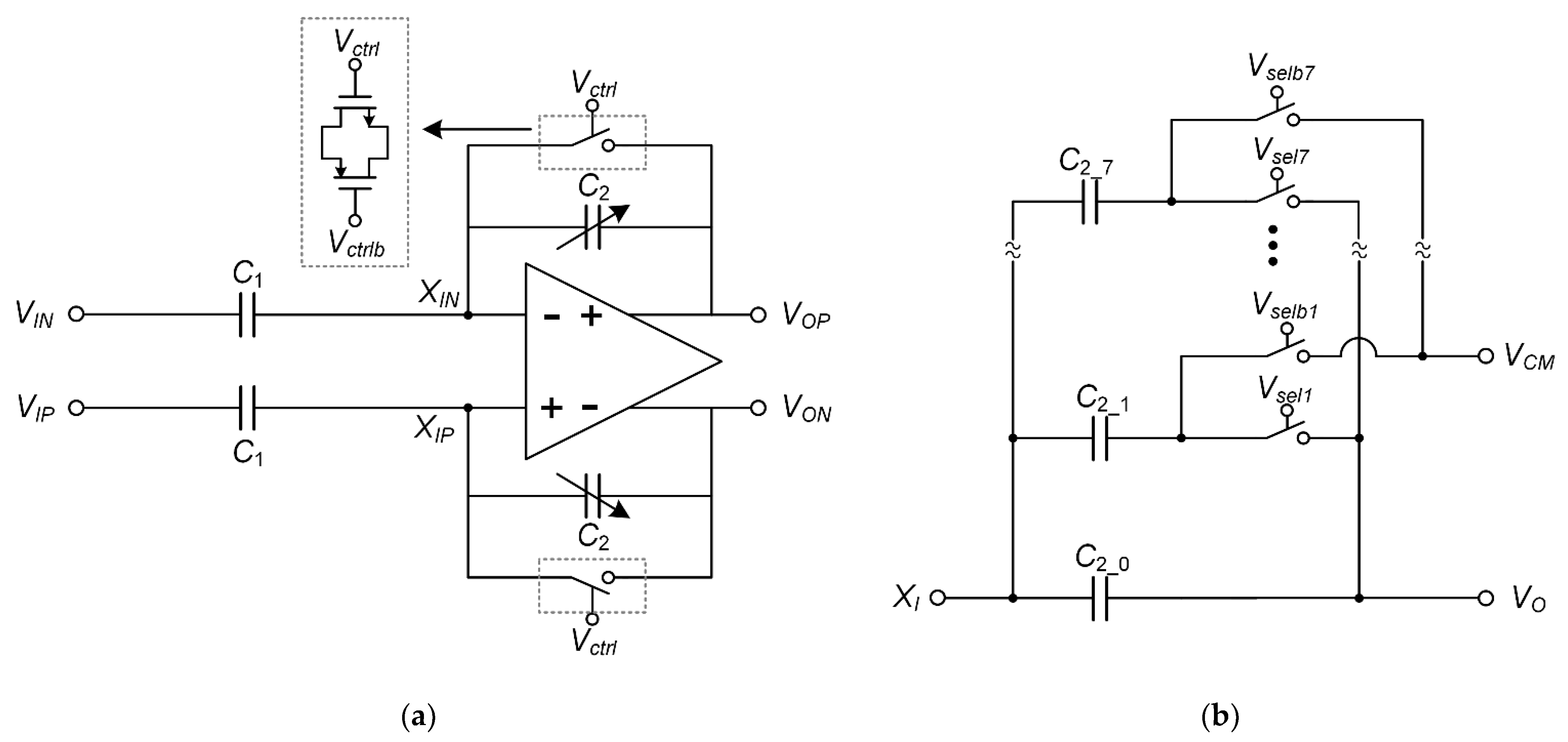
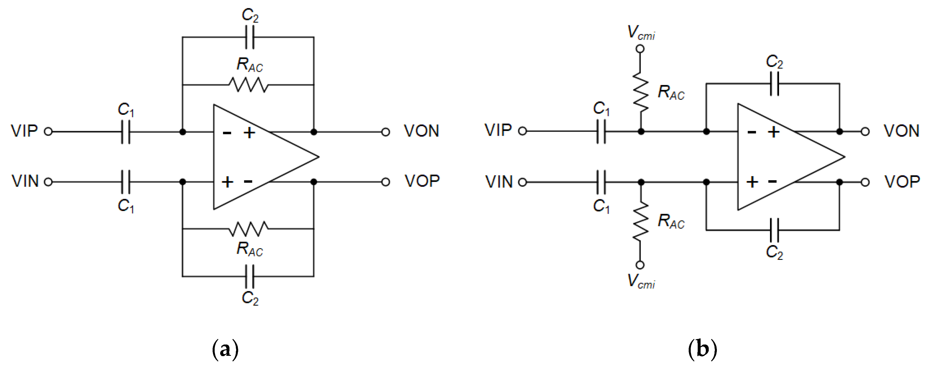
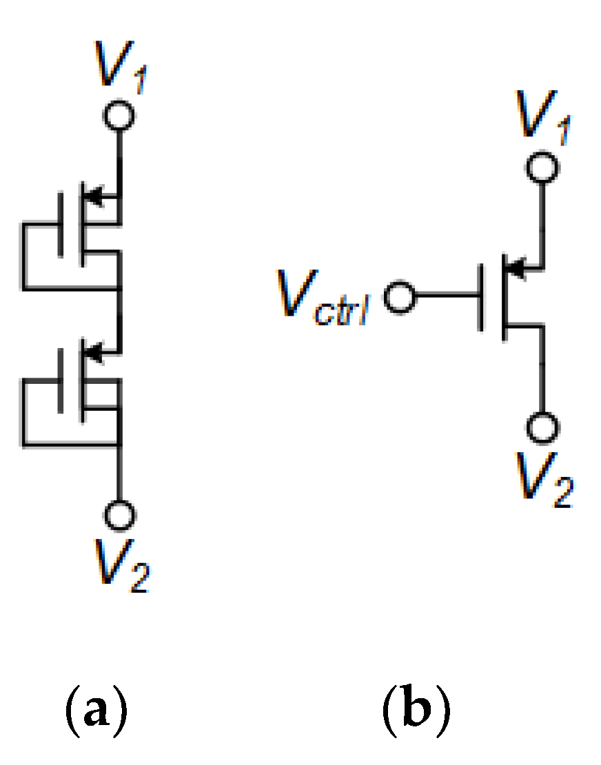
Figure 6a shows the architecture of the proposed microphone preamplifier. The switches are off during the normal operation of the preamplifier (Vctrl = 0), and they are turned on for a short period of time during the start-up (Vctrl = VDD). To reduce the nonlinear characteristics of the switches, the switches are realized as CMOS transmission gates, where the NMOS and PMOS have same size of W/L = 0.25 μm/0.15 μm. It can also reduce the charge injection when the switches are being turned off.
In this preamplifier, the gain is determined by C1/C2. Figure 6b shows the array of capacitors, out of which we select certain sub capacitors to get a desired C2. When designing the switching of sub capacitors, we need to consider the preamplifier output change at the gain-switching moment. If the output voltage does not change instantaneously to the new value that is proper for the new gain, this will lead to an offset in the differential output. Although this offset is eventually removed by the charge flow through RAC, it takes a very long time because of very large RAC. In the proposed scheme shown in Figure 6b, the top plates of the sub-capacitors (C2i) are always connected to the virtual ground (i.e., OTA input), while the bottom plates are switched between the preamplifier output node and the common-mode voltage. When the preamplifier gain is increased, the bottom plates of the selected sub capacitors are switched from the output to the common-mode voltage. Then, the charge stored in those capacitors moves to the capacitors whose bottom plate is still connected to the output node. This increases the output voltage to the level which is proper for the new gain. When the gain is lowered, the bottom plates of the selected sub capacitors are switched from the common-mode voltage to the output voltage. Then, the charge redistribution between the sub capacitors instantaneously lowers the output voltage to the level proper for the new gain. Note that before the switching, the capacitor whose bottom plate is switched from the common-mode output to the output node was fully discharged.
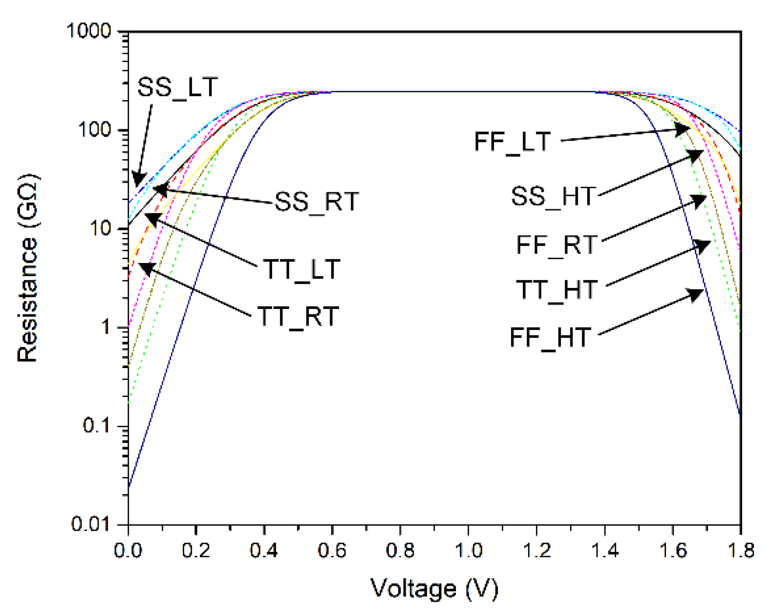
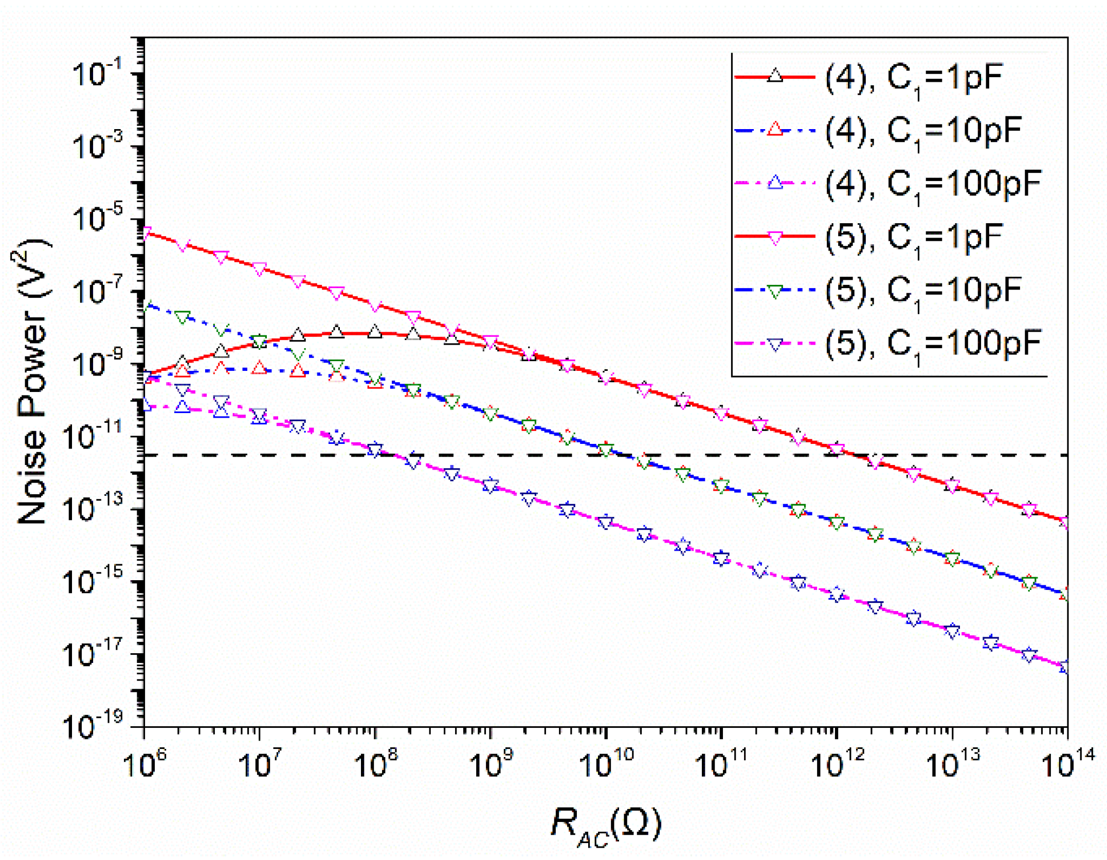
Figure 7 shows the simulated resistance of the pseudo-resistor. One of the terminals is connected to the common mode voltage of 0.9 V and the voltage of the other terminal is swept from 0 V to 1.8 V. A concern when using pseudo-resistors is the variation of the resistance. Therefore, we repeated simulations at three process corners (TT, FF, SS) and three temperatures (T = 25 °C, 27 °C, 85 °C). From Figure 7, we observe that in the off-state the resistance is about 250 GΩ regardless of the corner condition or the temperature, while it is affected by the conditions in the on-state or the sub-threshold range. We attribute this to the limitation of the PDK. Having admitted the limitation, we can still confirm that the resistance stays larger than 10 GΩ for 0.3 V < V < 1.6 V. Note that in the region where we become concerned about low resistance of the pseudo-resistor, the simulation results correctly predict corner-condition-and-temperature dependency. As mentioned above, when the voltage is between 0.6 V and 1.4 V, the resistance is about 250 GΩ. From the noise power discussion in the previous section, we observed that this value of resistance along with C1 = 10 pF could be used to limit the noise power to below N1 = 3.2 × 10⁻¹² V2, which is 10% of the total noise budget. However, we also note that 250 GΩ is not large enough to be used with C1 = 1 pF to satisfy the same noise requirement.
The preamplifier gain is programmable from 0 dB to 21 dB with 3 dB steps. To keep the input impedance constant for all gain settings, C1 was fixed at 10 pF and C2 was made programmable by selecting the desired capacitor from capacitor arrays.
It is important to select a proper OTA architecture to achieve the desired performance. For example, a telescopic architecture can be selected when a high gain OTA is required. If the supply voltage is low, an OTA with current source level shifting technique [16] or an OTA with an active load with cross-coupled bulk [17] can be selected. In our work, we adopted a two-stage pseudo class-AB OTA to realize a power efficient low noise OTA. 
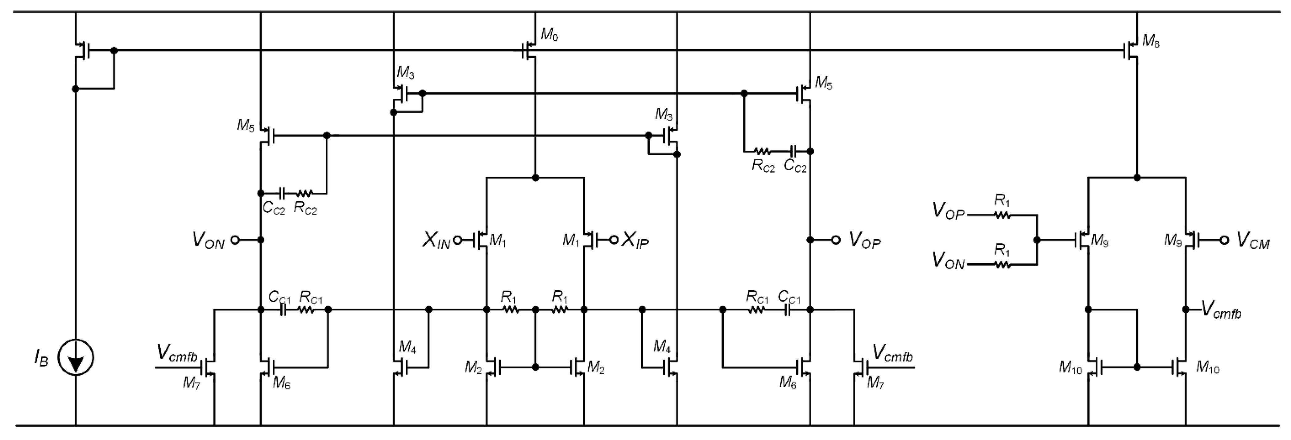
Figure 8 shows the schematic diagram of the OTA used in this work. The OCML of the first stage is stabilized by the resistor R1. A large resistance of R1 = 1 MΩ is used to prevent the open-loop gain reduction. The OCML of the OTA is stabilized by a common-mode feedback (CMFB) circuit employing a simple differential pair. The bias current IB was copied from the reference current that was generated by a conventional constant-gm circuit. 
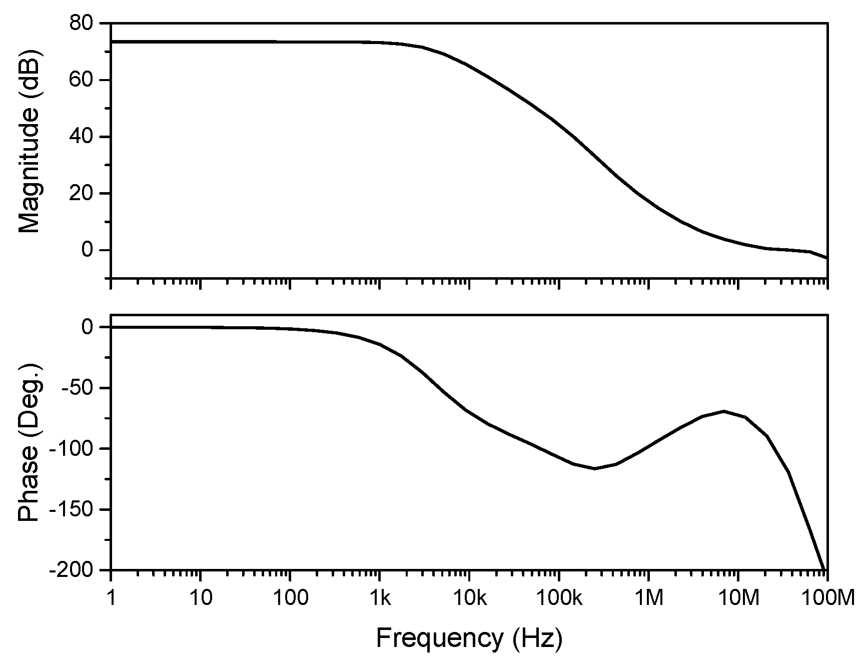
Figure 9 shows the AC simulation result of the OTA with the 10 kΩ load resistance. From the simulation, we observe that the loop gain and the phase margin are 73.4 dB and 61°, respectively. The size of the devices in the OTA is listed in Table 2. To reduce the flicker noise, we used large input transistors (W1/L1 = 1664 μm/3 um) and to minimize the thermal noise, gm2/gm1 was made small. Note that the large M1 and M2 lower the bandwidth of the OTA due to its large parasitic capacitances at the output nodes of the first stage. However, the large trans-conductance of the OTA required for a good SNR already leads to a unity-gain bandwidth much larger than the 20-kHz bandwidth of a microphone amplifier. Therefore, the large parasitic capacitance does not become a problem in our design.
The simulated A-weighted input-referred noise of the OTA in the signal bandwidth of 20 Hz < f < 20 kHz was 1.3 × 10⁻¹² V2, where the contribution by the thermal noise and the flicker noise were 40% and 60%, respectively. All transistors operate in the saturation region except for M1, which operates in the weak inversion region because of its large W/L ratio to obtain a large gm1.
The AC noise simulations of the pre-amplifier indicates that the total output noise is 2.2 × 10⁻¹¹ V2 (A-weighted) when the preamplifier gain is 0 dB. Of the total noise, the thermal noise and flicker noise contribution are 1.2 × 10⁻¹¹ V2 and 0.96 × 10⁻¹² V2, respectively. This corresponds to an A-weighted SNR of 101.6 dB. The noise from the pseudo-resistor is less than 1% of the total noise. Figure 10 shows the output spectrum obtained from the transient noise simulation of the proposed preamplifier with the gain of 0 dB with a 4.3 kHz, 800 mVpk,diff balanced input signal. From the result, we obtain the SNR and SNDR of 101.4 dB (A-weighted) and 94.7 dB (A-weighted), respectively.
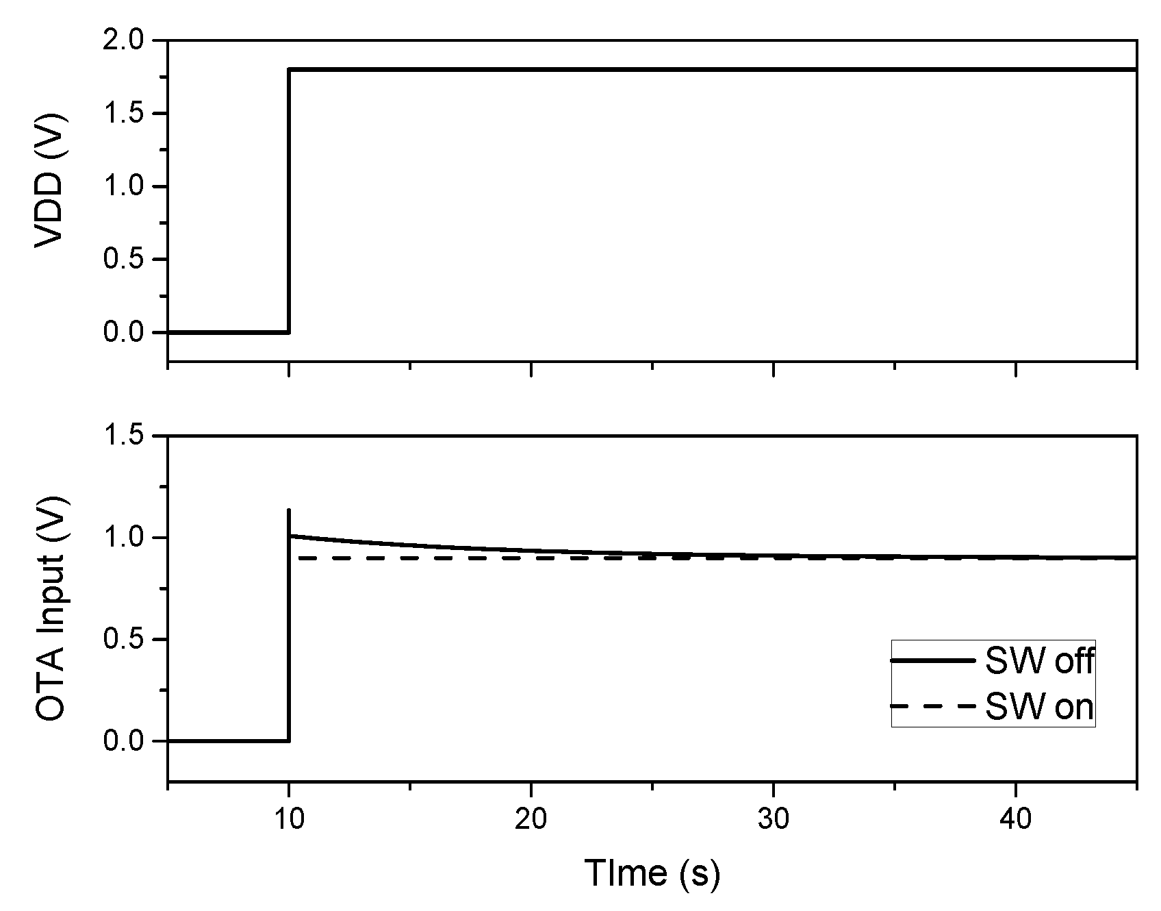
Figure 11 shows the results of the transient simulations of the preamplifier to observe the start-up behavior. The supply voltage is ramped up from 0 V to 1.8 V with a rising time of 1 μs at t = 10 s. When the switches stay off and behave as pseudo-resistors, the settling of the OTA input nodes is very slow, and the required settling time was tens of seconds. However, if the switch is turned on, the input node voltage of the OTA is stabilized very quickly with settling time of tens of microseconds. 
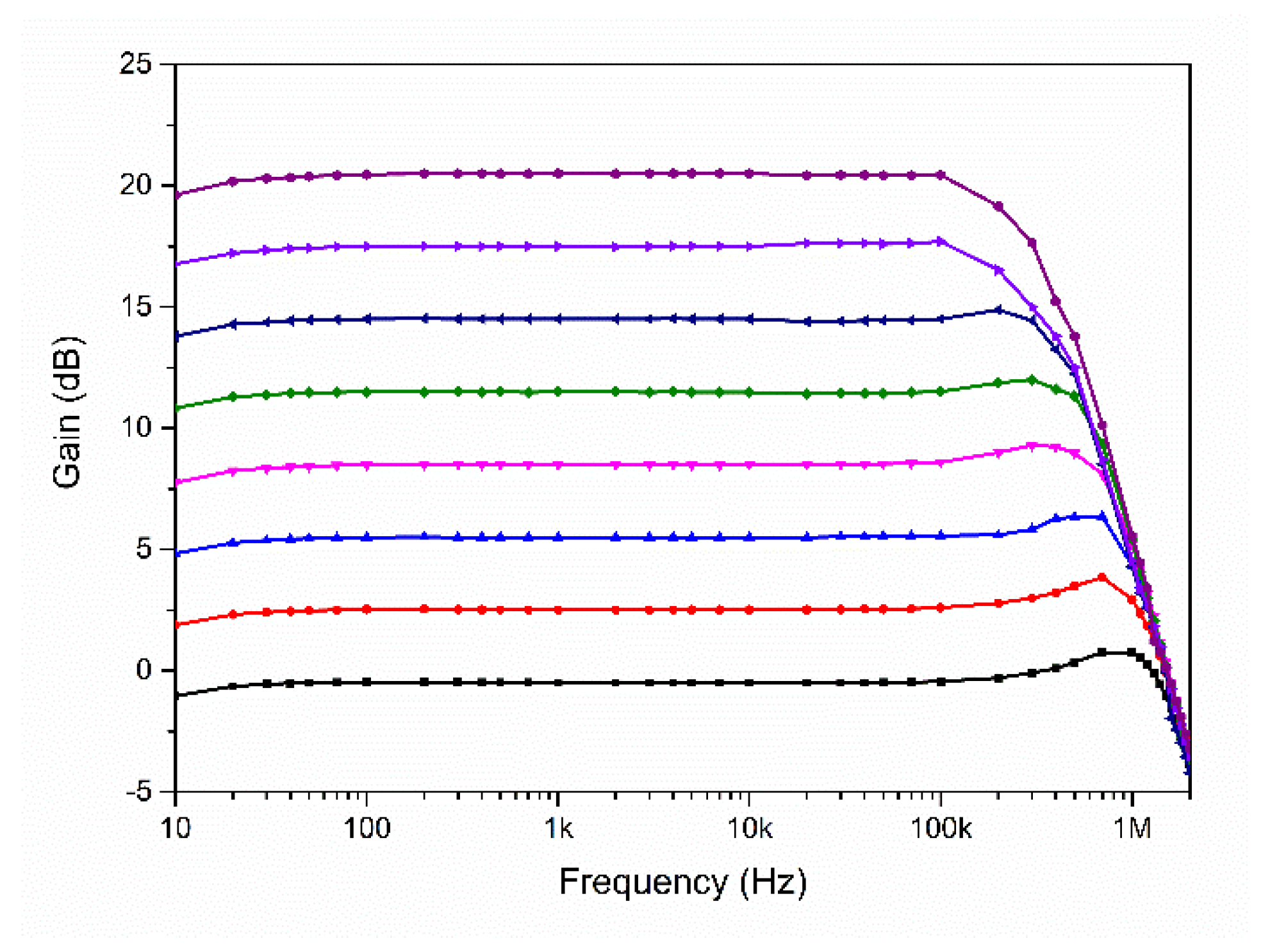
Figure 12 shows the frequency response of the preamplifier for all gain settings obtained from ac simulations. From the results, we observe that the lower cut-off frequency is lower than 1 Hz for all gain settings. In addition, we can observe flat frequency response over the audio bandwidth between 20 Hz and 20 kHz. In fact, the lower and upper 3 dB frequency of the frequency response is much lower than 20 Hz and higher than 20 kHz, respectively. The high upper 3 dB frequency is the result of a very large trans-conductance of the OTA, which is needed for a high SNR performance. When the upper 3 dB frequency is higher than necessary, a concern is that the noise in the extra bandwidth is aliased down to the signal band when sampled by a down-stream ADC and the SNR is degraded. However, in this work, we assumed an oversampling ADC with a large oversampling ratio, which is usually used for audio applications. In this case, the aliasing can be avoided and the noise in the extra bandwidth can be safely removed by a low-pass filtering decimation filter. The very low lower 3 dB frequency is the result of a very large RAC. As explained in Section 2.3, a large RAC is actually beneficial because it reduces the total noise in the signal band. Because the large resistance could be obtained easily using pseudo-resistors, we did not try to increase the lower 3 dB frequency.

4. Measurement Results and Discussion

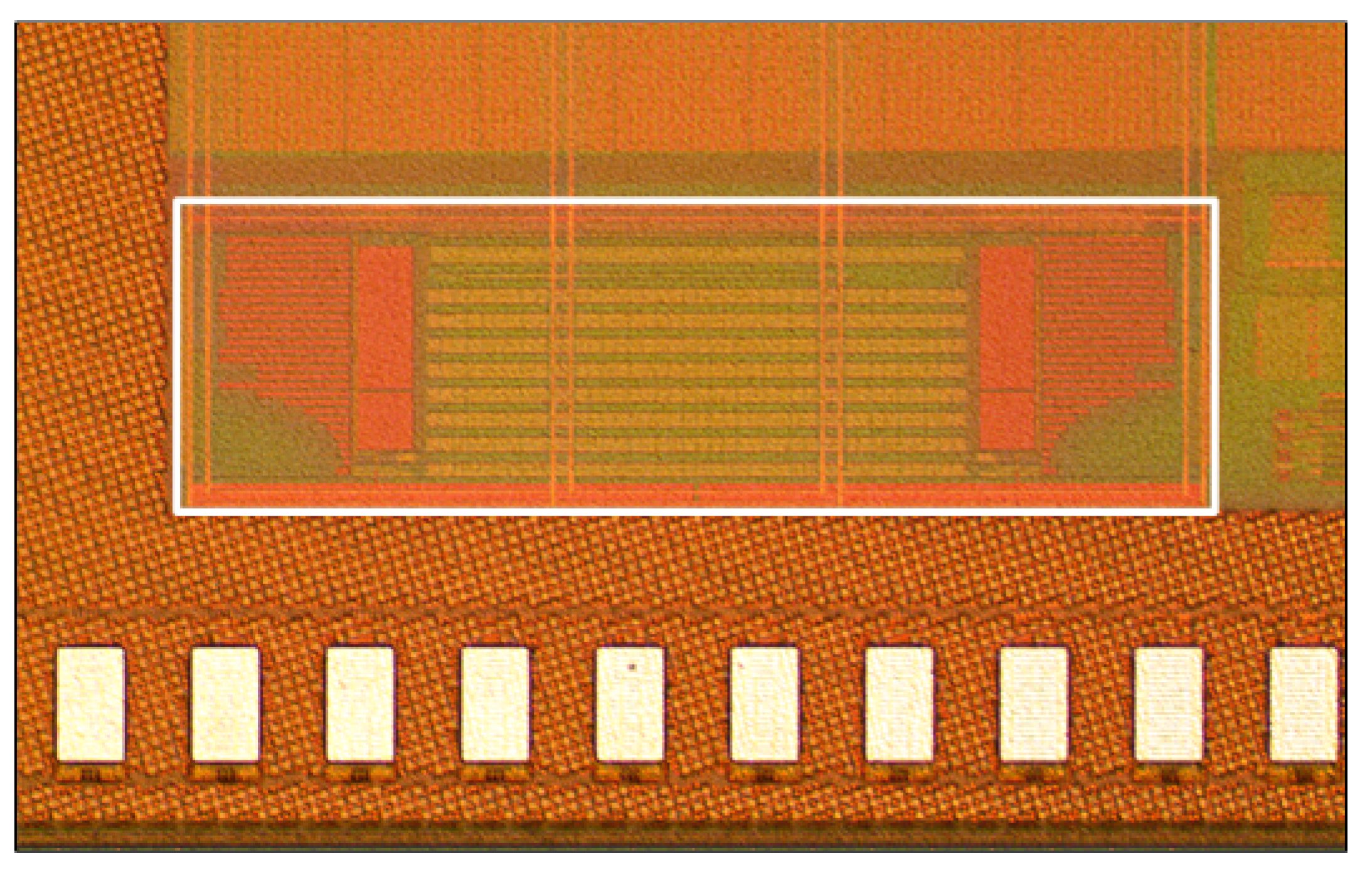
The proposed preamplifier was fabricated using a 28 nm CMOS technology. Figure 13 shows the chip microphotograph of the fabricated circuit. The white rectangle in Figure 13 indicates the preamplifier and the active area occupied by the preamplifier is 0.19 mm2.
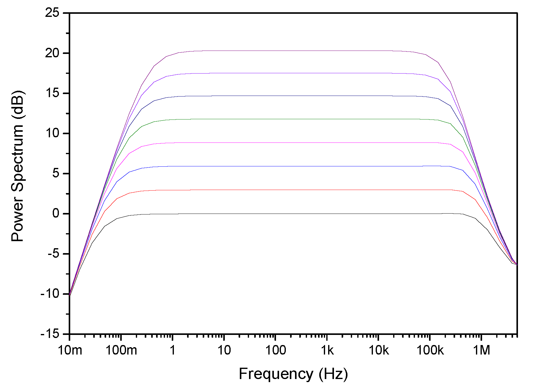
Figure 14 shows the frequency response with the balanced input signal with 1.8 V supply for all gain settings measured with an Agilent 81160A function generator and an Agilent MSO9104A oscilloscope. The measured data matches the simulation results of Figure 12 well, and very flat frequency responses were obtained in the audio band. The small reduction of gain in the low frequency range is from the limit of the measurement system, and the slight peaking at around 1 MHz is from the interaction of the large input capacitance of the measurement system and the output impedance of the preamplifier.
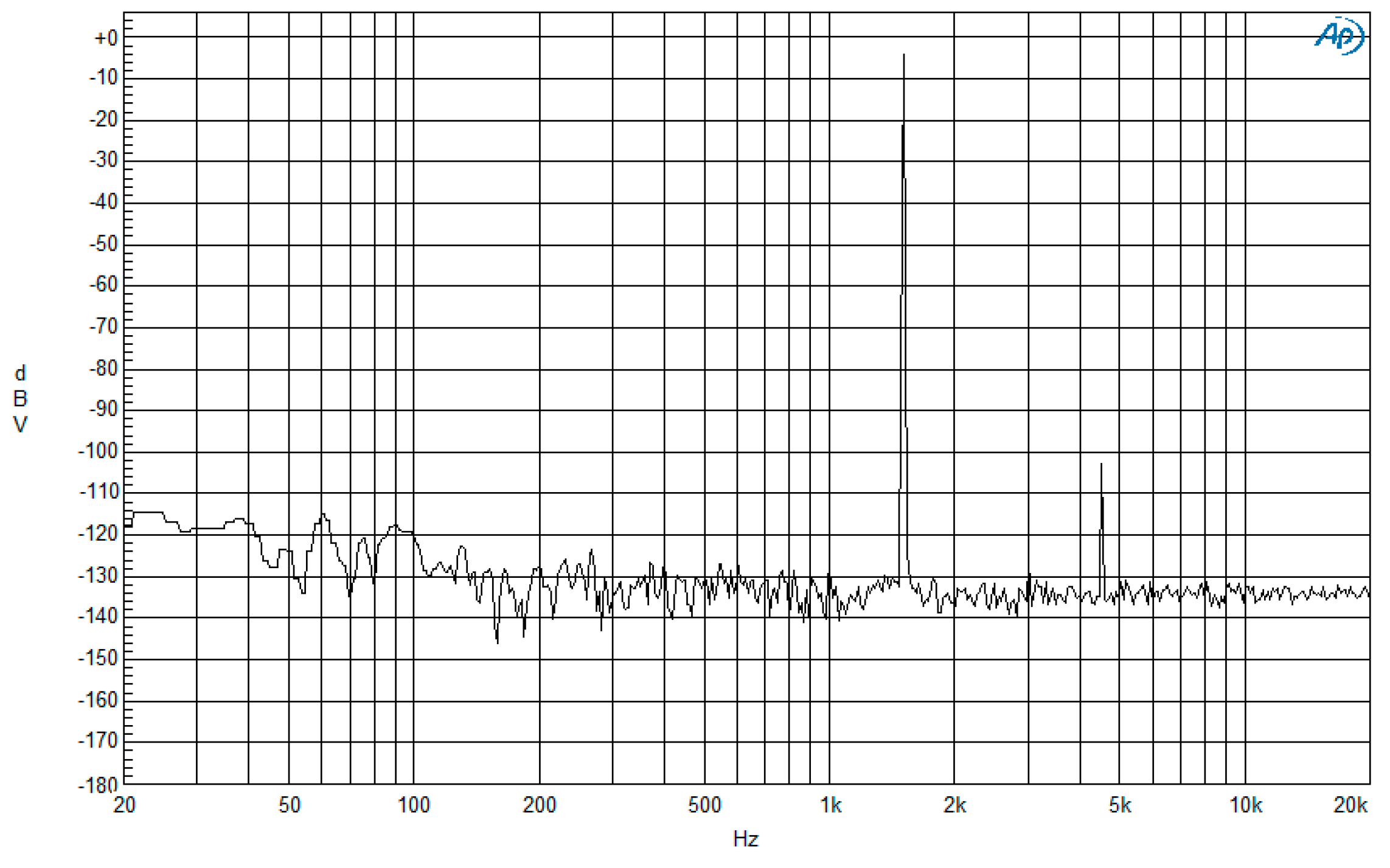
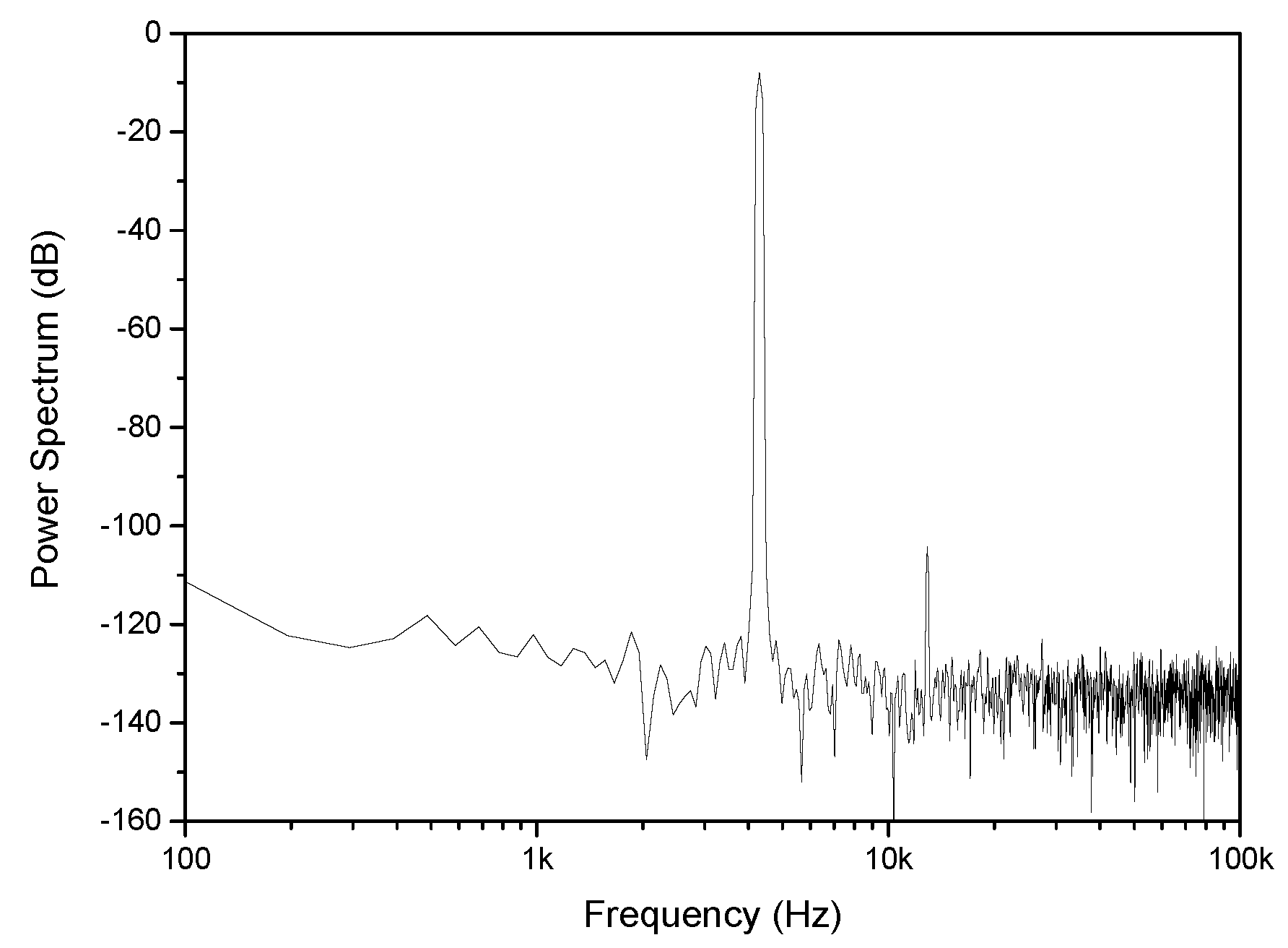
Figure 15 shows the output power spectrum of the preamplifier measured with the gain of 0 dB and 800 mVpk, 1.5 kHz sinusoidal input supplied by an Audio Precision AP-2700. The single-ended output of AP-2700 was converted to a differential signal by a balun consisting of a center-tapped transformer before being applied to the preamplifier. The supply voltage was 1.8 V. From the results, we can observe that the corner frequency of flicker noise is about 200 Hz due to the OTA’s large input transistors. The third order distortion is the dominant distortion component whose power is about 100 dB lower than the signal power. The powers of other harmonic components are lower than the signal power by more than 120 dB and is buried in the noise.
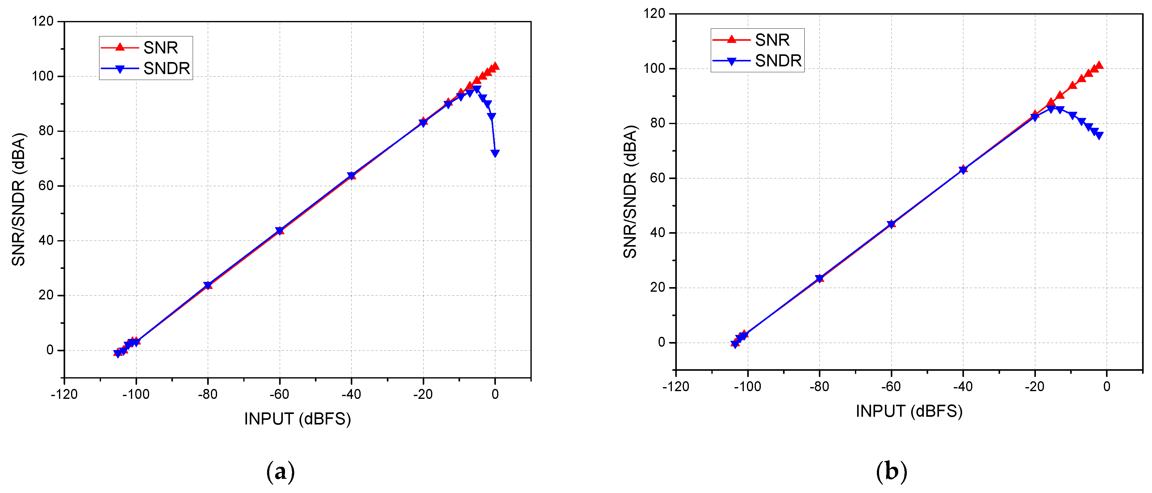
Figure 16 shows the measured A-weighted SNR and A-weighted SNDR versus input level when (a) the balanced signal was applied and (b) the single-ended signal was applied. The maximum A-weighted SNR and A-weighted SNDR with the balanced signal were 107 dBA and 95.5 dBA, respectively. The measured DR of the preamplifier is 107 dB. Maximum SNRs were obtained at the input signal level of 0 dBFS (=1.8 Vpk,diff), which produces the maximum output swing of 1.8 Vpk,diff. With a single-ended signal applied, the peak A-weighted SNDR was reduced to 85.6 dBA mainly due to even-order harmonics. However, the SNRs with a single-ended signal is almost identical to those with balanced input signal.
The measured power consumption with the supply voltage of 1.8 V was 270 μW. Table 3 summarizes measurement results of the preamplifier. In the table, we present A-weighted and unweighted SNR, SNDR, and DR for balanced and single-ended input signals with the gain of 0 dB and 21 dB. Comparisons with previously published results are provided in Table 4. The power-efficiency is compared by employing the figure of merit (FoM) factor, which is defined as FoM = DR + 10log10(Bw(Hz)/Power(W)). Since the gain of [5] is fixed at 20 dB, the SNR, SNDR, DR, and FoM of [5] was adjusted by adding the 20 dB gain for fair comparisons. From Table 4, we can observe that our design represents comparable performance with the state of the art designs. Ref. [5] reports the highest FoM among the comparisons. However, the resistive architecture of [5] limits the input impedance to 10 kΩ, and it employed external ac-coupling capacitor. Our work, as well as [8], both report capacitive on-chip ac-coupling preamplifiers. A pseudo-resistor was employed in our work to realize an on-chip ac-coupling, while switched capacitor networks were adopted as biasing resistors in [8].

5. Conclusions

In this work, a design of on-chip ac-coupling microphone preamplifier is presented. Since the architecture of the preamplifier greatly affects its performance, we compared the previously reported preamplifiers in terms of input impedance, noise performance, and the feasibility of on-chip ac-coupling. We chose the inverting architecture with capacitive feedback. An on-chip ac-coupling and a fast start-up time were achieved at the same time by adopting CMOS-transmission-gate switches as pseudo resistors. In the normal operation of the preamplifier, the switches are turned off for producing a very large resistance, whereas they are turned on for fast settling during the start-up. The proposed microphone preamplifier was designed and fabricated using a 28 nm CMOS process. To accommodate the various microphones and line-in signals, the preamplifier has a variable gain from 0 dB to 21 dB in steps of 3 dB. To minimize the power consumption, a two-stage pseudo class-AB OTA was employed. Measurement results showed that the preamplifier had a peak SNDR of 95.5 dBA and DR of 107 dBA with a power consumption of 270 μW.

Author Contributions

Conceptualization, S.I. and S.-G.P.; methodology, S.I. and S.-G.P.; validation, S.I. and S.-G.P.; formal analysis, S.I. and S.-G.P.; investigation, S.I. and S.-G.P.; writing—original draft preparation, S.I.; writing—review and editing, S.-G.P. All authors have read and agreed to the published version of the manuscript.

Funding

This research was funded by National R&D Program through the National Research Foundation of Korea (NRF) funded by Ministry of Science and ICT (No. 2020M3H2A1076786).

Acknowledgments

The CAD tools were provided by IC Design Canter (IDEC), Korea.

Conflicts of Interest

The authors declare no conflict of interest.

References

  1. Kuo, S.M.; Morgan, D.R. Active noise control: A tutorial review. Proc. IEEE 1999, 87, 943–973. [Google Scholar] [CrossRef] [Green Version]
  2. Elliott, S.J.; Curtis, A.R.D.; Bullmore, A.J.; Nelson, P.A. The active minimization of harmonic enclosed sound fields, part III: Experimental verification. J. Sound Vibrat. 1987, 117, 35–58. [Google Scholar] [CrossRef]
  3. Sukumaran, A.; Karanjkar, K.; Jhanwar, S.; Krishnapura, N.; Pavan, S. A 1.2V 285uA analog front end chip for a digital hearing aid in 0.13um CMOS. In Proceedings of the IEEE Asian Solid-State Circuits Conference (A-SSCC), Singapore, 11–13 November 2013; pp. 397–400. [Google Scholar]
  4. Kim, S.; Lee, S.J.; Cho, N.; Song, S.-J.; Yoo, H.-J. A fully integrated digital hearing aid chip with human factors considerations. IEEE J. Solid State Circuits 2008, 43, 266–274. [Google Scholar] [CrossRef]
  5. Song, S.; Lee, C.; Jang, M.; Chae, Y. A 185 μW −105.1 dB THD 88.6 dB SNDR Negative-R Stabilized Audio Preamplifier. In Proceedings of the IEEE 45th European Solid State Circuits Conference (ESSCIRC), Cracow, Poland, 23–26 September 2019; pp. 261–264. [Google Scholar]
  6. Kim, S.; Cho, N.; Song, S.; Yoo, H. A 0.9 V 96 uW fully operational digital hearing aid chip. IEEE J. Solid State Circuits 2007, 42, 2432–2440. [Google Scholar] [CrossRef]
  7. Im, S.; Park, S.-G. A 154-uW 80-dB SNDR analog-to-digital front-end for digital hearing aids. Analog. Integr. Circuits Signal Process. 2016, 89, 383–393. [Google Scholar] [CrossRef]
  8. Barbieri, A.; Nicollini, G. 100+dB A-weighted SNR microphone preamplifier with on-chip decoupling capacitors. IEEE J. Solid State Circuits 2012, 47, 2737–2750. [Google Scholar] [CrossRef]
  9. Van Rhijn, A. Integrated circuits for high performance electret microphones. In Proceedings of the 114th AES Convention, Amsterdam, The Netherlands, 22–25 March 2003. [Google Scholar]
  10. Amplifiers for 3 Wire Analog Electret Microphones; LMV1032-06/LMV1032-15/LMV1032-25 Data Sheet; Texas Instrument: Dallas, TX, USA, 2013.
  11. Acoustic Components & Accessoties; Hosiden. Available online: https://hbl.co.uk/wp-content/uploads/2016/01/Acoustic_ComponentAccessorie.pdf (accessed on 7 July 2021).
  12. Acoustic Interface Design Guide; Knowles. Available online: https://www.mouser.com/datasheet/2/218/07-KA-895_designguide_final_v1-1120.pdf (accessed on 7 July 2021).
  13. Harrison, R.R.; Charles, C. A low-power low-noise CMOS amplifier for neural recording applications. IEEE J. Solid State Circuits 2003, 38, 958–965. [Google Scholar] [CrossRef]
  14. Um, J.-Y.; Sim, J.-Y.; Park, H.-J. A Gate-leakage insensitive 0.7-V 233-nW ECG amplifier using non-feedback PMOS pseudo-resistors in 0.13-um N-well CMOS. J. Semicond. Technol. Sci. 2010, 10, 309–315. [Google Scholar] [CrossRef]
  15. Delbruck, T.; Mead, C.A. Adaptive photoreceptor with wide dynamic range. Proc. IEEE Int. Symp. Circuits Syst. 1994, 4, 339–342. [Google Scholar]
  16. Renteria-Pinon, M.; Ramirez-Angulo, J.; Dias-Sanchez, A. Simple scheme for the implementation of low voltage fully differential amplifiers without output common-mode feedback network. J. Low Power Electron. Appl. 2020, 4, 34. [Google Scholar] [CrossRef]
  17. Ballo, A.; Grasso, A.D.; Pennisi, S. Active load with cross-coupled bulk for high-gain high-CMRR nanometer CMOS differential stages. Wiley Int. J. Circuit Theory Appl. 2019, 47, 1700–1704. [Google Scholar] [CrossRef]
Figure 1. Block diagram of microphone and preamplifier.
Electronics 10 01624 g001
Figure 2. Architecture of (a) resistive inverting preamplifier and (b) resistive non-inverting preamplifier.
Electronics 10 01624 g002
Figure 3. Architecture of capacitive preamplifier with (a) the RAC placed between the input terminal and output terminal of the OTA and (b) the RAC placed at the virtual ground of the OTA.
Electronics 10 01624 g003
Figure 4. Output noise from (4) and (5) versus RAC with several C1 (= C2).
Electronics 10 01624 g004
Figure 5. (a) A pseudo-resistor consisting of two diode connected MOSFETs, (b) a MOSFET switch as a pseudo-resistor.
Electronics 10 01624 g005
Figure 6. (a) Architecture of the proposed microphone preamplifier and (b) schematic diagram of the capacitor array for C2.
Electronics 10 01624 g006
Figure 7. Resistance of the transmission gate switch in the off state simulated at three process corners (TT, SS, FF) and three temperatures (LT = −25 °C, RT = 27 °C, HT = 85 °C).
Electronics 10 01624 g007
Figure 8. Schematic diagram of the OTA.
Electronics 10 01624 g008
Figure 9. AC simulation results of designed OTA.
Electronics 10 01624 g009
Figure 10. Power spectrum from a transient noise simulation of the proposed preamplifier.
Electronics 10 01624 g010
Figure 11. Transient simulation results of start-up operation.
Electronics 10 01624 g011
Figure 12. Simulation results of frequency response of the proposed preamplifier for all gain settings.
Electronics 10 01624 g012
Figure 13. Microphotograph of the fabricated preamplifier.
Electronics 10 01624 g013
Figure 14. Measured frequency response of the preamplifier with the balanced input signal.
Electronics 10 01624 g014
Figure 15. Output spectrum of preamplifier for G = 0 dB with 800 mVpk, 1.5 kHz balanced sinusoidal input.
Electronics 10 01624 g015
Figure 16. Measured SNR and SNDR of preamplifier versus input level (A-weighted). (a) When the balanced signal was applied and (b) when the single-ended signal was applied with preamplifier gain of 0 dB.
Electronics 10 01624 g016
Table 1. Target specifications.
ParameterTarget Specification
Supply Voltage1.8 V
Bandwidth20 Hz–20 kHz
Peak SNR (A-weighted)>100 dB
Input impedance>500 kΩ
Table 2. Size of the devices for the OTA.
DeviceSizeDeviceSizeDeviceSize
M0414 μm/1 μmM48 μm/6 μmRC111 kΩ
M11664 μm/3 μmM5300 μm/1.5 μmCC14 pF
M2800 μm/20 μmM6 = M775 μm/1.5 μmRC26 kΩ
M316 μm/6 μmR11 MΩCC210 pF
Table 3. Summary of the measured performance.
Input SignalGainSNDRpkDRSNDRpk *DR *
Balanced0 dB95.6 dB103.4 dB95.5 dBA107 dBA
21 dB77.6 dB82.9 dB80.3 dBA86 dBA
Single-ended0 dB95.5 dB102.1 dB85.6 dBA104.6 dBA
21 dB77.2 dB82.5 dB79 dBA86 dBA
*: A-weighted.
Table 4. Performance comparison.
ParameterThis Work[8][5]
Process28 nm40 nm65 nm
ArchitectureCapacitiveCapacitiveResistive
Ac-couplingOn-chipOn-chipExternal
Supply Voltage (V)1.81.51.2
Gain (dB)0 to 210 to 19.520
Peak SNDR (dB)95.5101108.6 dB *,+
Peak DR (dB)107106109.3 dB *,+
FoM (dB)185.7183.8189.6 +
Power Consumption (μW)270330185
Active Area (mm2)1.190.190.12
*: Unweighted. +: Adjusted to the gain of 0 dB
Publisher’s Note: MDPI stays neutral with regard to jurisdictional claims in published maps and institutional affiliations.

