Article

Compact 2 × 2 Circularly Polarized Aperture-Coupled Antenna Array for Ka-Band Satcom-on-the-Move Applications

1
TELNET Redes Inteligentes, 50198 Zaragoza, Spain
2
Department of Electronic Engineering and Communications, Universidad de Zaragoza, 50009 Zaragoza, Spain
*
Author to whom correspondence should be addressed.
Electronics 2021, 10(14), 1621; https://doi.org/10.3390/electronics10141621
Submission received: 10 June 2021 / Revised: 29 June 2021 / Accepted: 5 July 2021 / Published: 7 July 2021
(This article belongs to the Special Issue Antenna Design and Integration in Wireless Communications)

Abstract

:
This paper presents a novel design of a wideband circular polarization 2 × 2 microstrip antenna array working at Ka-band frequencies, from 27.5 to 31 GHz. This module is highly integrable with new silicon beamformer chips, creating a unit cell that can be part of a large electronically steerable antenna for compact, ultra-low-profile, Satcom-on-the-move (SOTM) platforms. A multi-layer structure fabricated in standard printed circuit board (PCB) technology with high-yield substrates has been used. The radiating elements consist of double-stacked circular patches housed in a cavity and fed by H-shaped aperture coupling. It achieves a bandwidth of 16.5 % with a wide beam-width of 95° in the desired band, which is necessary for wide scanning angles in a large phased array. In the 2 × 2 unit cell, the antenna elements are distributed by means of a sequential rotation technique where the separation between two of them is 5.3 mm in the XY-plane. Broadside beam-widths ranging from 53.4° at 27.5 GHz to 42.1° at 31 GHz are achieved, with boresight directivities from 10.7 to 12.9 dBi, respectively, in both the RHCP and LHCP polarization. Moreover, mutual coupling levels below −20 dB and an axial ratio less than 3 dB in the whole band guarantee a good circular polarization purity.

1. Introduction

The interest in satellite communications has grown exponentially in recent years. With the massive deployment of non-geostationary orbit (NGSO) LEO/MEO satellite constellations, a great variety of high-speed and low-latency communication applications are showing up [1,2,3,4]. The upcoming scenario is driving the development of new antenna front-ends capable of tracking one or more satellites while providing a high data rate and low-latency two-way communications. Traditionally, tracking GEO satellites has been a relatively easy task, since a parabolic antenna pointed towards the satellite position can provide good communication with the satellite transceiver, and mechanical steering could provide uninterrupted communication with the satellite. However, the antenna front-end configuration is not that simple for NGSO networks, where satellites are moving with respect to the land-terminal. Although tracking the satellite as it moves may seem easily solved with a mechanical structure that follows its movement, which is the basic principle of Satcom-on-the-move (SOTM), the satellite eventually crosses the horizon and the antenna must perform a handover to track a new satellite in the line of sight. Mechanical systems show very poor behavior at switching between satellites, with very slow responses that imply periodic losses of the communication link, thus greatly reducing their reliability.
In this context, active antenna arrays with electronical steering are a great alternative to mechanical positioners. These terminals can achieve response times of the order of one millisecond to continuously track the satellite or to perform a satellite handover with a much faster response without the need for mechanical actuators. Another major advantage of these active antenna terminals is that they do not require a parabolic structure to achieve the needed directivity. Therefore, the use of these systems allows for the design of ultra-low-profile devices, which has driven the uprise of a great amount of new SOTM applications, such as unmanned aerial vehicle, connected cars, commercial flights, and other scenarios where satellite communications is the only choice.
In particular, in recent years, great efforts have been made on the development of new Ka-band SOTM terminals for land mobile, maritime or aeronautical platforms that require low-profile antenna front-ends capable of providing high data rate and low latency of the order of 10 milliseconds from emerging LEO/MEO satellite networks, compared to the 300 or more milliseconds latency with GEO satellites. In this context, phased array antennas, also known as active electronically scanned arrays (AESAs), play an important role owing to their characteristics of low profile, size and weight, and high reliability because there are no moving parts to fail. AESAs can also steer beams in microseconds and support multiple, simultaneous, and independent beams [5,6].
One key difficulty in the design of Ka-band Satcom front-ends is the compact and cost-effective integration in a single PCB of the antenna elements with the high number of active and passive radio frequency (RF) components such as low noise amplifiers (LNAs), power amplifiers (PAs), phase shifting devices, hybrid couplers, etc., that require not only good thermal handling but also considerable mounting space and adequate power consumption. The maturity reached by microwave monolithic integrated circuits (MMICs) and the latest advances in silicon technologies such as SiGe or CMOS have helped to address this challenge for a large-scale deployment [7,8].
Nowadays, a way to solve the integration problem is placing the antennas on-chip, as in [9], where a W-band 4 × 4 wafer-scale phased array has been developed and reported. However, it is important to note that this approach requires identical sizes for the chip and the antenna aperture to be efficient, making it very useful at frequencies above 60 GHz, and to drastically reduce the price of phased arrays.
Nevertheless, for frequencies below 60 GHz, there are other alternatives that combine printed circuit boards (PCB), surface mount technology (SMT) and silicon beamformer chips, resulting in a cost-effective solution alternative. As shown in Figure 1, in this configuration the radiating elements are typically placed on one side of the PCB, while the opposite side is employed to mount all SMD devices, so that the chips can be placed very close to the radiating elements, which minimizes feed losses and maximizes the gain-to-noise-temperature (G/T) of the antenna receiver and the effective isotropic radiated power (EIRP) of the antenna transmitter.
The proposed 2 × 2 circularly polarized antenna Tx array is based on this concept and some examples can be found in the literature [9,10]. In [11,12], dual-band phased arrays are presented to cover Tx/Rx satellite communications, interleaving in the same space K/Ka-band radiating elements with Ka-band elements, but introducing new integration problems that they will have to solve and with reduced bandwidths of 4.3% in Tx (29.5–30.8 GHz) and 4.8% in Rx (20.2–21.2 GHz).
Focusing on this type of RF beamforming structure, in the literature we find state-of-the-art beamformers which include low-noise amplifiers (LNA), power amplifiers (PA), phase shifters, variable gain amplifiers (VGAs), power combiners, simple pole double throw (SPDT) switches, together with SPI control and even biasing networks all in a single chip, working at frequencies up to 95 GHz, for 4, 8 or 16 channels, and with a high yield [13,14,15]. To feed the beamformers array, an RF distribution network is implemented with cascaded Wilkinson dividers so that all chips are fed with a balanced RF signal.
On the other hand, regarding the antenna radiating elements, many techniques have been developed to improve the circular polarization radiation bandwidth at the Ka-band, which include air- or substrate-integrated cavity-backed structure [16,17], stacked patches [18], aperture-coupled patches [19] and multilayered structures [20,21]. Microstrip antennas are commonly used due to their great advantages in terms of simplicity, versatility and low profile, while they are inexpensive and easy to manufacture [22].
Three different single circularly polarized radiating elements with different beam-widths and working at 30 GHz have been investigated in [23]. The first design implements a classical microstrip patch antenna fed through a U-shaped slot and where the circular polarization is achieved by trimming opposite corners. The second and third use the same radiating element but are inserted in a cavity and enclosed by folded conducting walls, respectively. In [24], an antenna element using aperture-coupled stacked patches and a fork-based feeding network in asymmetric stripline technology, from 17.6 to 30.3 GHz, is presented. Their main advantage resides in the fact of having a single radiating element with a good circular polarization over a great bandwidth. However, this can limit the beamforming performance in a phased array at some frequencies.
In this work, a circularly polarized, sequentially rotated, aperture-coupled antenna array with highly integrable, cost-effective silicon beamformers is proposed for SOTM applications. The 2 × 2 antenna array presented in this work will be the basic modular unit of a full Ka-band AESA.
This paper is organized as follows: Section 2 describes the system architecture, the antenna fabrication technology and the proposed multilayer stack-up. Section 3 shows the experimental measurements of the radiating element, discusses its design and performance, and provides a complete experimental characterization of the 2 × 2 antenna array configuration. Finally, conclusions are drawn in Section 4.

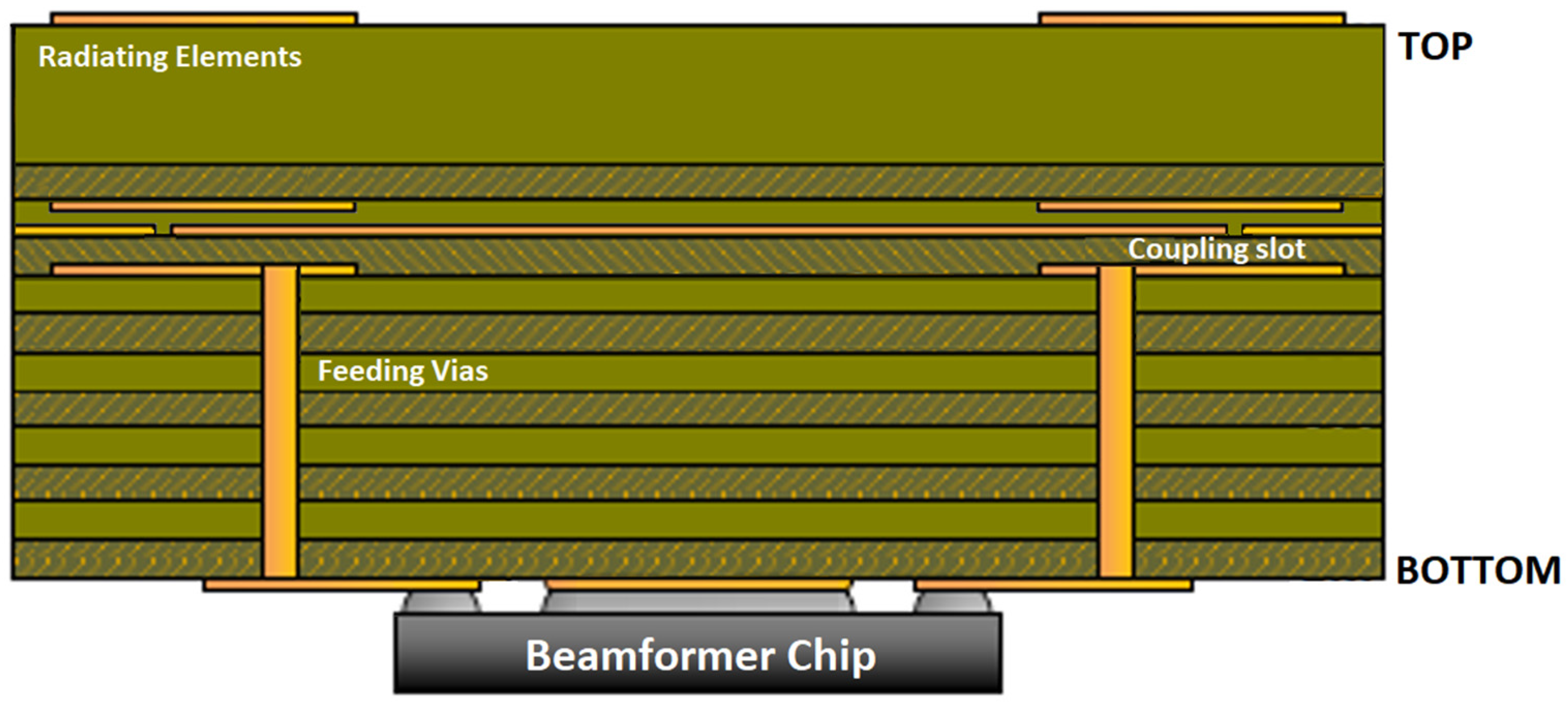
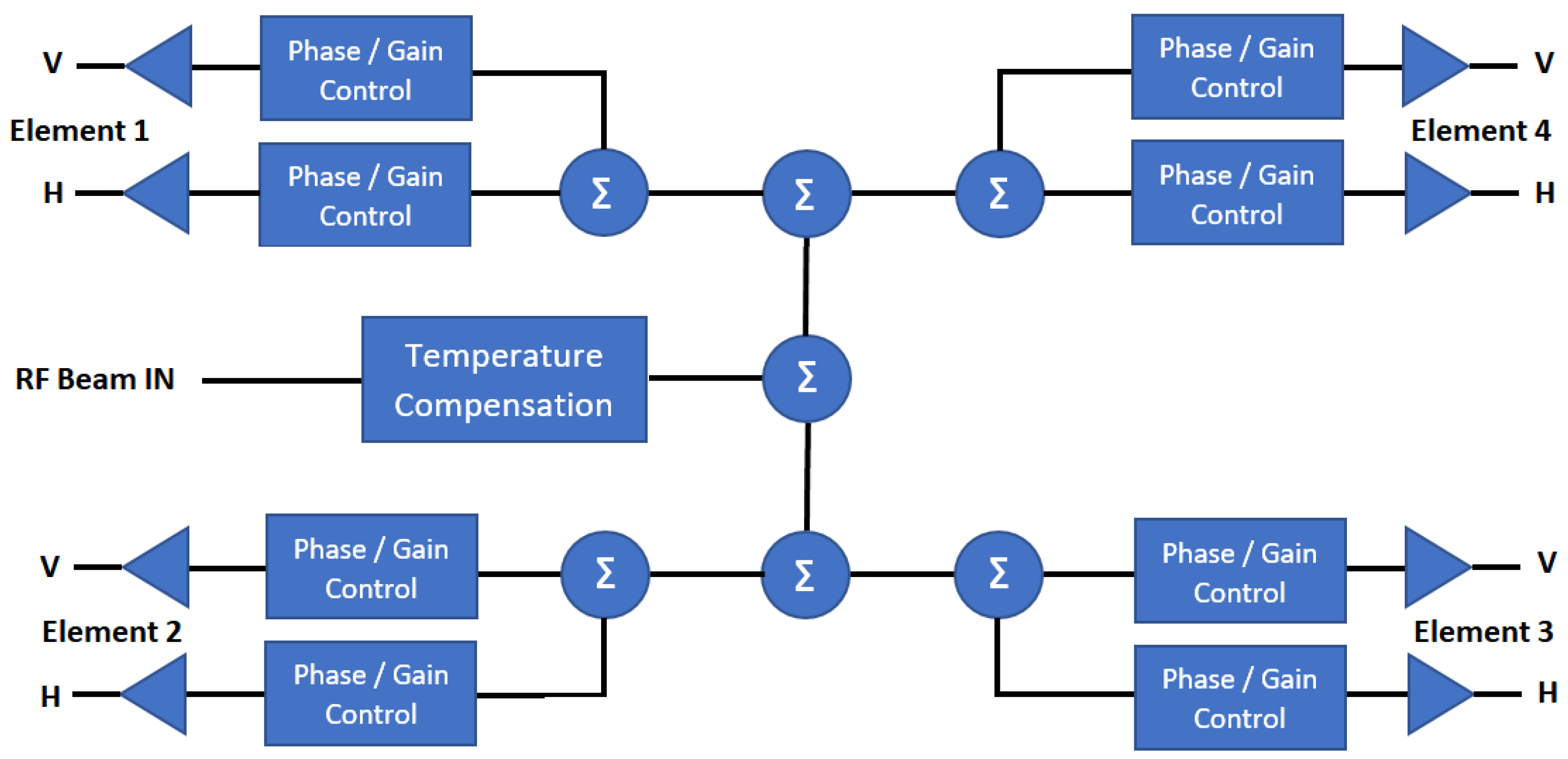
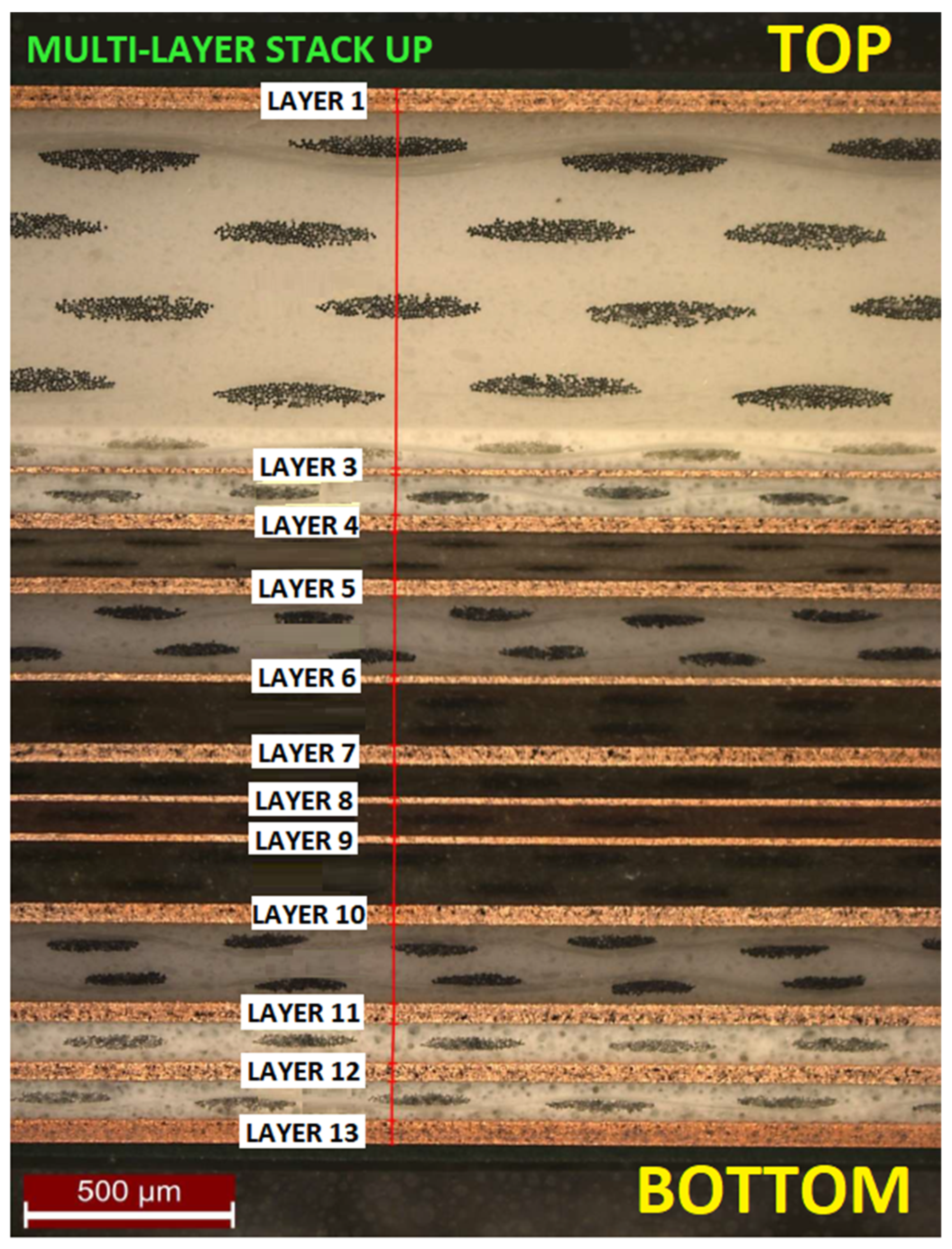
2. Antenna Array Design

The Ka-band transmit beamformer chip, shown in Figure 2, is based on a SiGe BiCMOS technology and consists of eight identical channels that feed the orthogonal polarizations of four radiating elements of the phased array.
Each channel contains a power amplifier, a variable gain amplifier with 16 dB gain control and a phase-shifter programmable with a 5-bit control. At the frequency range of operation from 27.5 to 30 GHz, the maximum gain per channel is 22 dB with a 12 dBm compression point at 1 dB (P1dB), while the total power consumption at P1dB is 1.35 W from a 1.8 V voltage supply.
Within current flat antenna technologies, a multilayer structure printed circuit board (PCB) has been chosen for the overall design, due to its low cost and mass production approach. Figure 3 shows a microphotography of a transversal cut of the manufactured PCB, in which the multi-layer stack-up structure consists of thirteen copper layers and different dielectric substrates, alternating cores and prepregs.
This PCB can be divided into four functional parts: Antenna elements are implemented using layers from L1 to L6. Layers L6 to L10 are used for routing DC power and the serial-peripheral interface (SPI) bus to program the beamformer chips. Layers L10 to L12 are assigned to the RF signal distribution network in stripline technology with integrated Wilkinson power dividers, and finally, layers L12 to L13, interconnection lines between PCB and surface mount components in grounded coplanar waveguide (GCPW) technology, are integrated.
To carry out the design, digital and DC layers are fabricated using FR4 substrates because of its lower cost, while the rest of the structure employs ceramic materials from Rogers and Isola with relative dielectric constants of 3.6 and low losses at high frequencies to achieve a better RF performance. This combination results in obtaining the advantages of high gain, low cost, and easy processing.
Vertical transitions are fabricated by through-hole, blind or buried vias, and micro-via connections with a diameter of 0.2 and 0.15 mm, respectively, creating coaxial-like structures to ensure the RF signal integrity [25]. In this kind of structure, it is known that the electric field is more tightly constrained inside the ground vias as the amount of these increases [26]. For this reason, the number of grounded vias implemented in the design corresponds to the maximum allowed if fabrication rules are considered.

Radiating Element Design

In this subsection, the antenna radiating element structure will be described. The radiating element, which is shown in Figure 4, is based on double-stacked circular patches, a 2.7 mm diameter driven patch (L1) and a 2.3 mm diameter parasitic patch (L3), which are surrounded by an artificial metallic wall formed by twenty vias (L1 to L3) whose diameter is 200 µm. The stacked patches technique is used to enhance the impedance bandwidth, while cavity backing is employed for surface wave suppression.
This element works at Ka-band frequencies, from 27.5 to 31 GHz, with a double circular polarization, switchable by means of electronic control circuitry. To achieve this, the driven patch is fed by electromagnetic coupling in two orthogonal points through both H-shaped slots. The aperture-coupled feeding technique has advantages such as no physical contact between the feed and radiator, wider bandwidths, and better isolation between feeding points.
Likewise, the input feeding network which excites each aperture is made up of a 50 Ω ground coplanar waveguide (GCPW) trace, a quasi-coax vertical transition, and a stripline to the H-slot. It is especially important to use the coaxial-like structures to provide reliable and high-performance vertical transitions between layers L5 and L13, where eight vias allocated in a 500 µm radius circle are used to surround the vertical transition to create a pseudocoaxial waveguide.

3. Experimental Results

The prototypes have been fabricated in a multilayer PCB with the highest performance and tolerances provided by the manufacturer Lab Circuits.

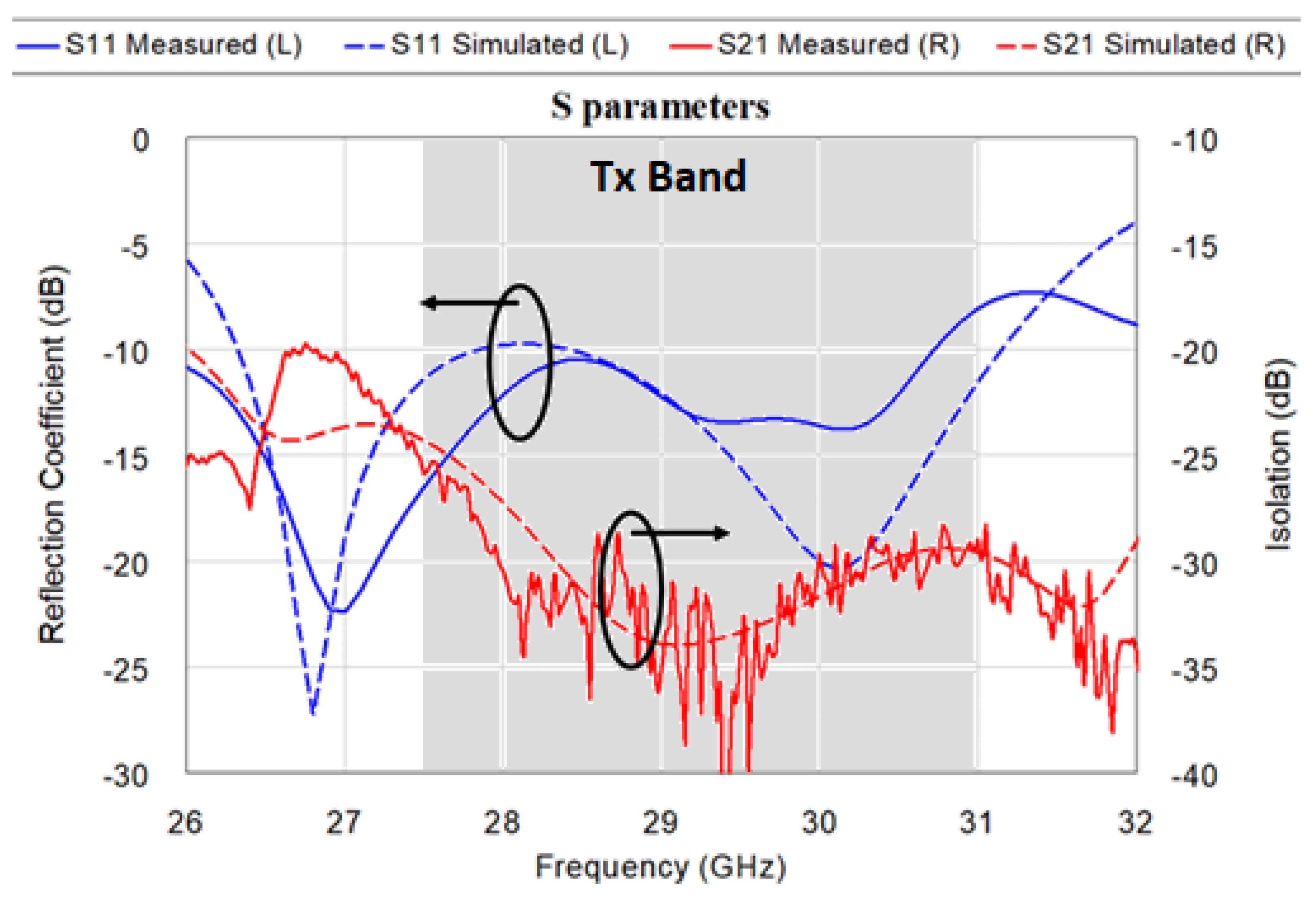
3.1. Single Radiating Element

The S-parameters of a single radiating element, which are shown in Figure 5 and Figure 6, have been measured using a 40 GHz vector network analyzer. The radiating element achieves a 10 dB impedance bandwidth that is roughly 16.5 %, which is greater than the Ka-band requires, and it overcomes the bandwidth achieved in recently published works, such as [27,28], 5%, and [29]. The isolation between ports is lower than −25 dB from 27.5 to 31 GHz. Simulation and measurement outcomes are quite similar, although there are slight differences owing to fabrication tolerances and measurement errors, as well as the uncertainty in the dielectric constant parameter of dielectric substrates at 30 GHz, whose value can be influenced by other characteristics such as the material anisotropy, the substrate thickness, or the copper roughness.
In order to measure the circular polarization radiation pattern of the manufactured radiating element prototype, a beamformer chip is assembled to feed the orthogonal polarizations of each radiating element. This beamformer chip includes a 5-bit phase control and a 5-bit gain control for each of its eight channels, in a 6 mm × 6 mm QFN package.
To generate the RHCP and LHCP radiation patterns, we feed the input ports with the same RF signal but with a phase shift between the vertical and horizontal polarization of 90° or −90°, respectively. The RHCP and LHCP normalized radiation patterns in the φ = 0° plane at 28 and 30 GHz are depicted in Figure 7. The measurement results show a ripple caused by the measurement system effect as well as the finite ground plane of the prototype that produces edge diffraction. For both polarizations, 28 and 30 GHz co-polar components show a maximum directivity of 6.5 dBi with a wide beam-width of about 95°.

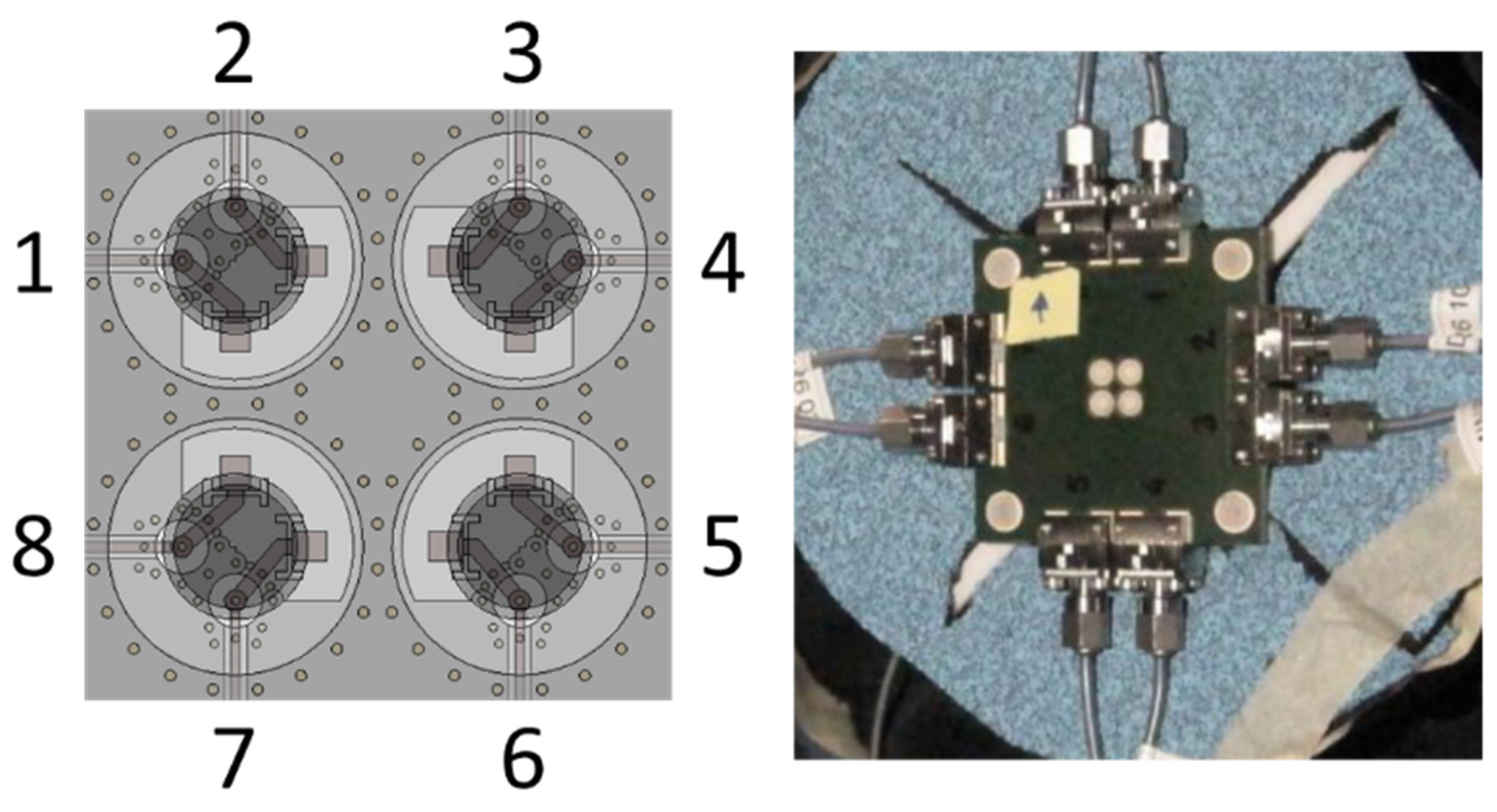
3.2. 2 × 2 Array Performance
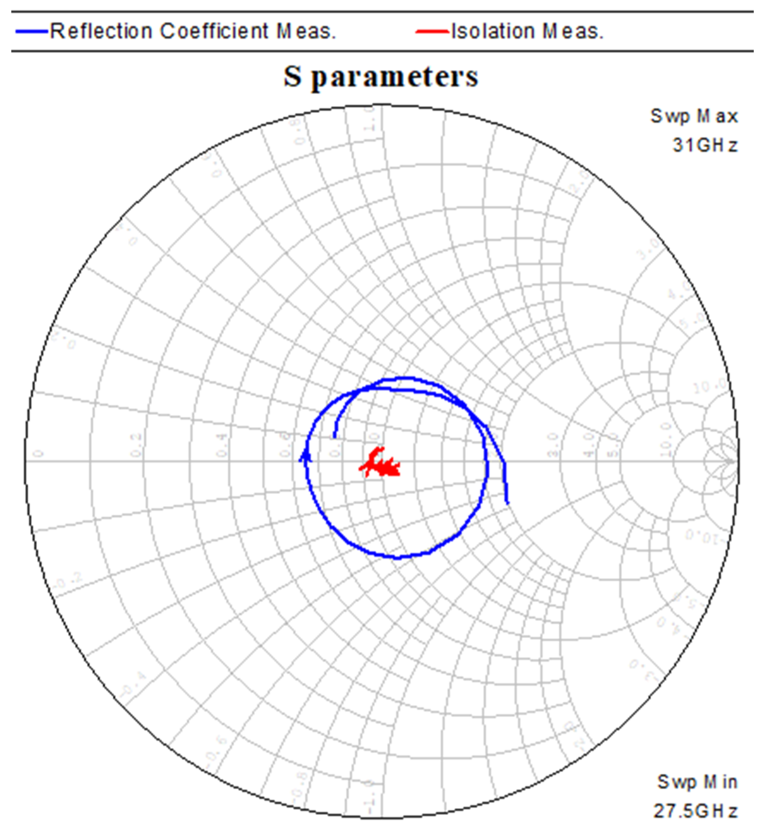
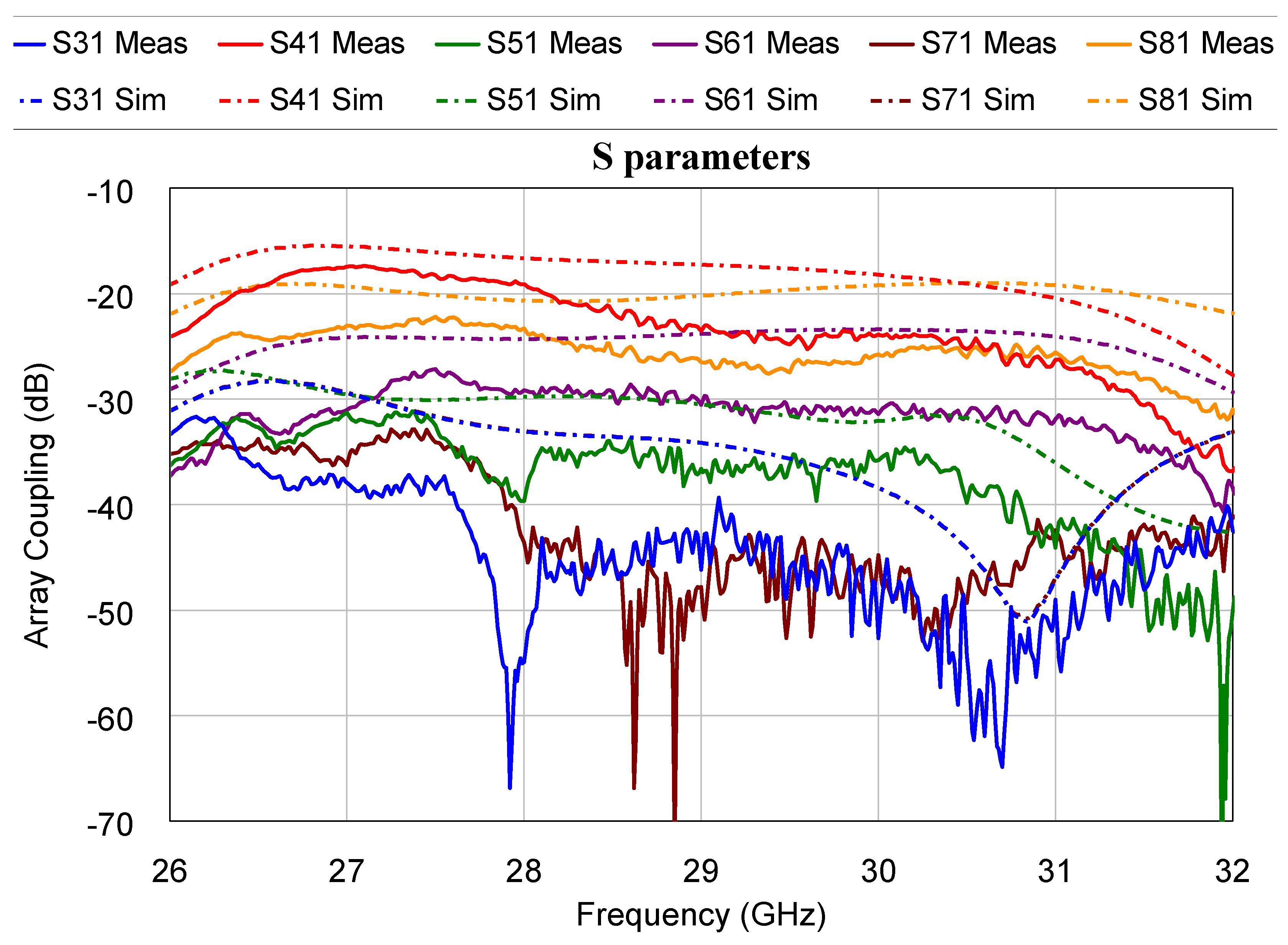
The 2 × 2 array shown in Figure 8 is the basic unit cell of the Ka-band transmitter. In the 2 × 2 array, the antenna elements are configured by using a sequentially rotated manner, where two adjacent radiators are separated by 5.3 mm. This configuration leads to an improvement of both polarization purity and radiation pattern symmetry [30], and its size allows for the subsequent assembly of the MMIC component on the bottom side of the PCB.
The complete Ka-band antenna will be built with many of these unit cells, so to maintain the distance of 5.3 mm between antenna elements, the 2 × 2 array must not be larger than 10.6 mm × 10.6 mm. Because of this, the H-slots (L4) and the input ports in the bottom layer are orthogonally placed in order to achieve the integration of the whole feeding network, from chipset to patch, in a minimum space.

3.2.1. Coupling

It is well known that a smaller spacing between elements is desirable for a compact array because it helps to suppress the grating lobes when scanning. Although a half-wavelength spacing minimizes the grating lobes, due to multiple factors, it might not be possible to achieve this integration density. For example, the size of the beamformer chips that must be placed on the opposite face of the PCB limits the density of radiating elements, because it is very challenging to bring the chips nearer and still have room for the RF distribution or DC biasing. Furthermore, a smaller spacing results in higher coupling between antenna elements. In Figure 9, mutual coupling outcomes for the antenna array are plotted.
To keep a low active reflection coefficient and acceptable axial ratio of the beam scanning array, mutual coupling levels should be lower than −20 dB [31]. Looking at Figure 5, it is clear that almost all the S-parameters are able to meet this condition in the frequency of interest, showing a worst case of −18 dB in a small frequency band from 26.5 to 28 GHz. Besides, it is verified that the mutual coupling is reduced when the frequency increases because the electrical distance between the radiating elements also increases.

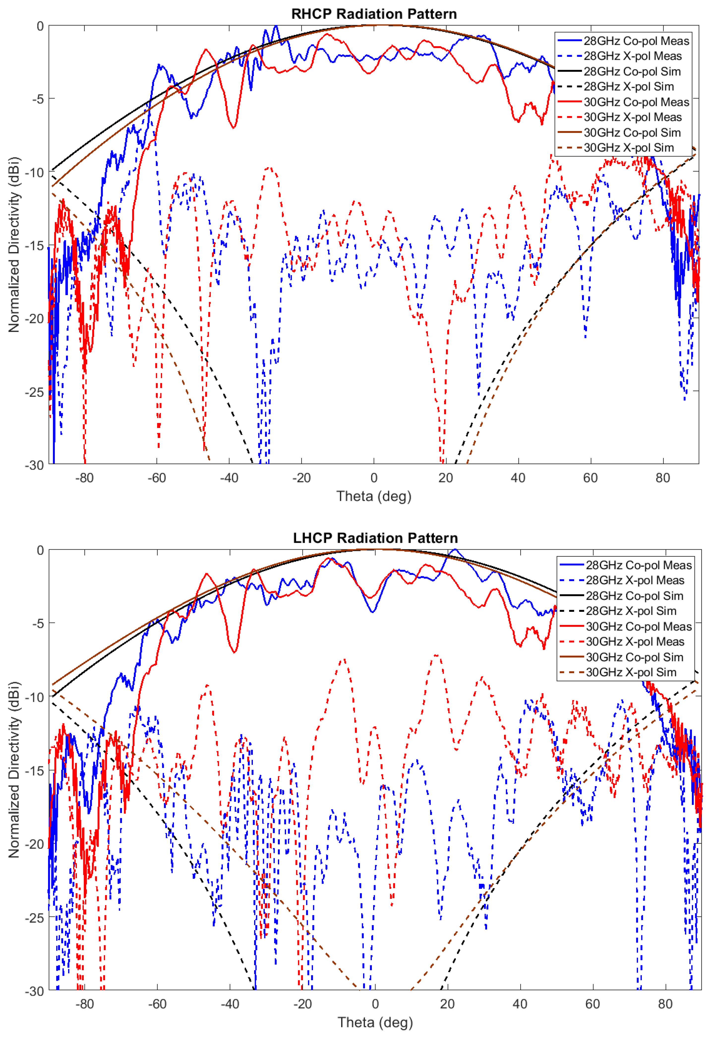
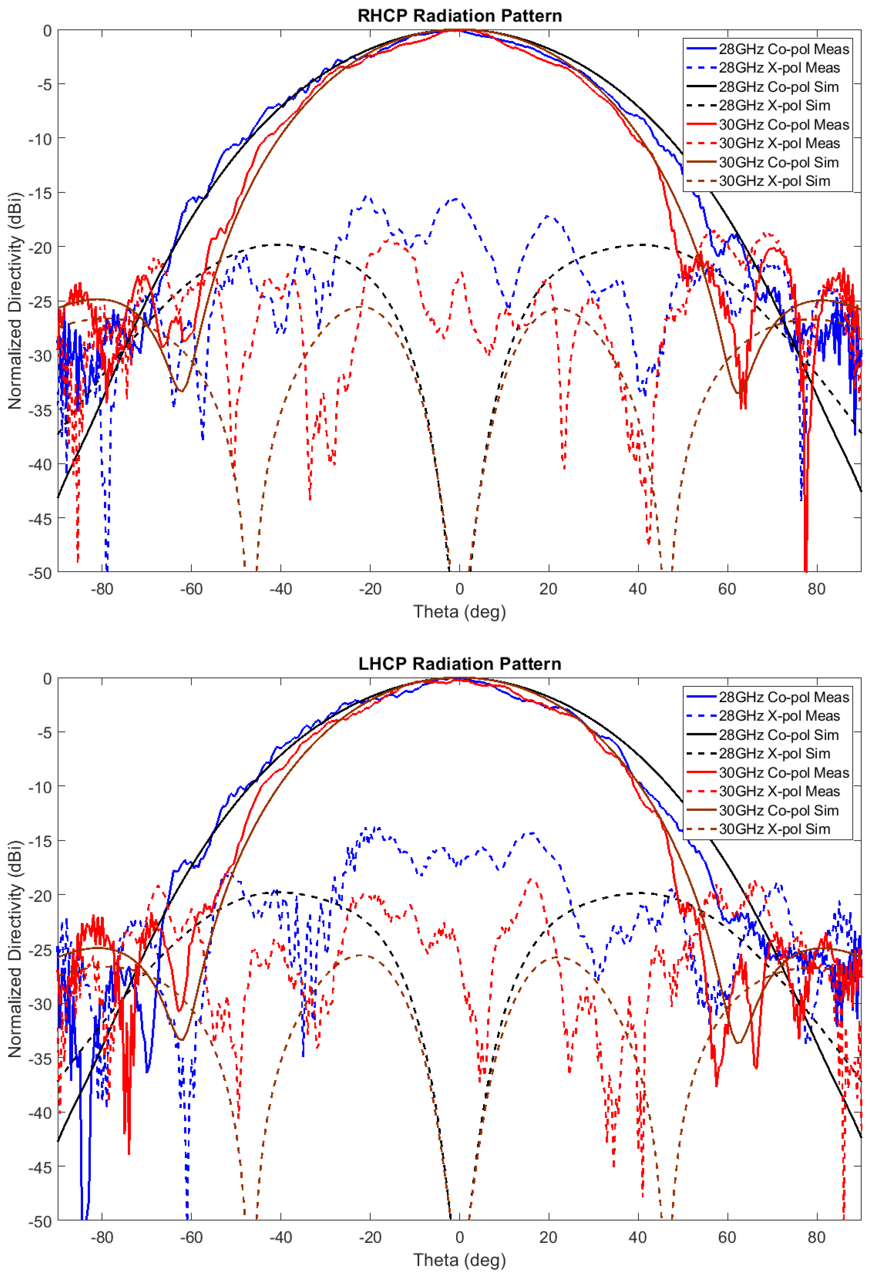
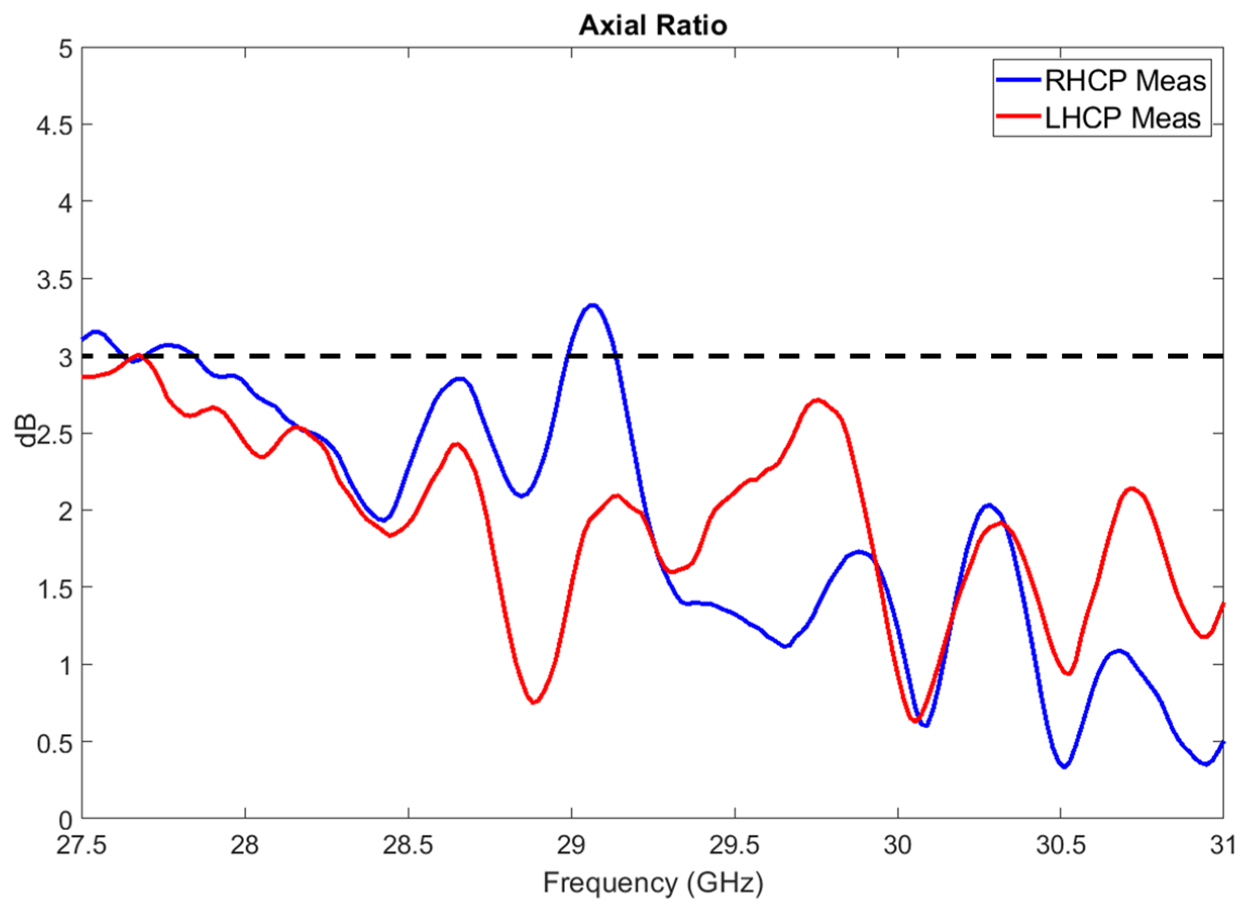
3.2.2. Radiation Parameters

To carry out the circular polarization radiation parameters measurements, we connect and program the beamformer chip to feed the patches with the same amplitude RF signal, and different phase. Figure 10 shows the normalized radiation patterns in the φ = 0° cut at 28 and 30 GHz for the RHCP and LHCP.
Co-polar results present a beam-width in the range of 53.4° (27.5 GHz) to 42.1° (31 GHz) with directivity values in boresight that varies from 10.7 dBi to 12.9 dBi, respectively. Good cross-polar discrimination levels below −15 dB are also achieved.
Lastly, Figure 11 shows the axial ratio in boresight as a function of frequency for both polarizations, RHCP and LHCP. In the whole band of interest, values below 3 dB are achieved, ensuring a good circular polarization purity. These data improve when frequency increases.

4. Discussion

In this work, a new design of a wideband and wide beam-width circularly polarized 2 × 2 antenna array covering the full Ka-band, from 27.5 to 31 GHz, has been proposed. The proposed design is well suited for integration with cost-effective silicon beamformer chips, and it is aimed at implementing wide scanning angles in Ka-band transmit antennas in mobile platforms.
The antenna array has been fabricated and a complete experimental characterization has been provided in this paper. The results are in good agreement with simulations, although there are some discrepancies caused by fabrication tolerances, measurement errors, and the uncertainty of the material properties in the Ka-band.
With the aim of reaching a compromise between price and performance, in a reduced area and a low profile, the design has been implemented in a planar technology using a standard multilayer PCB manufacturing process. Several techniques to improve performance have been applied, such as stacked patches, aperture coupling, cavity backing and a sequential rotation configuration. Thus, with a radiating element that yields a bandwidth of 16.5%, the 2 × 2 antenna array provides a wide beam-width ranging from 53.4° to 42.1°, while the maximum directivity varies between 10.7 and 12.9 dBi. Mutual coupling less than −20 dB and an axial ratio below 3 dB at all frequencies are obtained.

Author Contributions

Conceptualization, methodology, 3D modelling, multi-layer PCB stack-up definition, investigation, simulations, and experimental validation was carried out by H.B., G.R. and I.B.; H.B. carried out the original draft preparation and G.R. contributed to the writing of the paper. F.J.C. and S.C. were in charge of the project supervision and funding acquisition. All authors have read and agreed to the published version of the manuscript.

Funding

This work was partially supported by Spanish MINECO-FEDER project RTC2019-007039-7.

Data Availability Statement

Data is contained within the article.

Conflicts of Interest

The authors declare no conflict of interest.

References

  1. Marcellini, L.; Lo Forti, R.; Bellaveglia, G. Future developments trend for Ku and Ka antenna for satcom on the move. In Proceedings of the 5th European Conference on Antennas and Propagation (EUCAP), Rome, Italy, 11–15 April 2011; pp. 2346–2350. [Google Scholar]
  2. Borisov, S.; Shishlov, A. Antennas for Satcom-on-the-move, review. In Proceedings of the 2014 International Conference on Engineering and Telecommunication, Moscow, Russia, 26–28 November 2014. [Google Scholar]
  3. Safavi-Naeini, S.; Slekys, A.G. Electronic beam-scanning technology for small satellite communication systems and their future development. In Handbook of Small Satellites; Pelton, J., Ed.; Springer: Berlin/Heidelberg, Germany, 2020; pp. 527–553. [Google Scholar]
  4. Vaccaro, S.; Diamond, L.; Runyon, D.; Vigano, M.C. Ka-band mobility terminals enabling new services. In Proceedings of the 8th European Conference on Antennas and Propagation (EuCAP 2014), The Hague, The Netherlands, 6–11 April 2014; pp. 2617–2618. [Google Scholar]
  5. Kilic, O.; Zaghloul, A.I.; Kohls, E.C.; Gupta, R.K.; Jimenez, D. Flat antenna design considerations for satellite-on-the move and satel-lite-on-the-pause (SOTM/SOTP) applications. In Proceedings of the 2001 MILCOM Proceedings Communications for Network-Centric Operations: Creating the Information Force, McLean, VA, USA, 28–31 October 2001; Volume 2, pp. 790–794. [Google Scholar]
  6. Baggen, L.; Holzwarth, S. Satcom-on-the-move: Digital beam forming versus phased array. In Proceedings of the 8th European Conference on Antennas and Propagation (EuCAP 2014), The Hague, The Netherlands, 6–11 April 2014; pp. 2610–2614. [Google Scholar]
  7. Rebeiz, G.M.; Paulsen, L.M. Advances in SATCOM phased arrays using silicon technologies. In Proceedings of the 2017 IEEE MTT-S International Microwave Symposium (IMS), Honololu, HI, USA, 4–9 June 2017; pp. 1877–1879. [Google Scholar]
  8. McMorrow, R.; Corman, D.; Crofts, A. All silicon mmW planar active antennas: The convergence of technology, applications, and architecture. In Proceedings of the 2017 IEEE International Conference on Microwaves, Antennas, Communications and Electronic Systems (COMCAS), Tel-Aviv, Israel, 13–15 November 2017. [Google Scholar]
  9. Kibaroglu, K.; Sayginer, M.; Phelps, T.; Rebeiz, G.M. A 64-element 28-GHz phased-array transceiver with 52-dBm EIRP and 8–12-Gb/s 5G link at 300 meters without any calibration. IEEE Trans. Microw. Theory Tech. 2018, 66, 5796–5811. [Google Scholar] [CrossRef]
  10. Stoneback, M.; Madsen, K. A planar all-silicon 256-element Ka-band phased array for high-altitude platforms (HAPs) application. In Proceedings of the 2018 IEEE/MTT-S International Microwave Symposium—IMS, Philadelphia, PA, USA, 10–15 June 2018; pp. 783–786. [Google Scholar]
  11. Sandhu, A.I.; Arnieri, E.; Amendola, G.; Boccia, L.; Meniconi, E.; Ziegler, V. Radiating elements for shared aperture Tx/Rx phased arrays at K/Ka band. IEEE Trans. Antennas Propag. 2016, 64, 2270–2282. [Google Scholar] [CrossRef] [Green Version]
  12. Amendola, G.; Arnieri, E.; Boccia, L.; Ziegler, V. Annular ring slot radiating element for integrated millimeter wave arrays. In Proceedings of the 2012 6th European Conference on Antennas and Propagation (EUCAP), Prague, Czech Republic, 26–30 March 2012; pp. 3082–3085. [Google Scholar]
  13. Shahramian, S.; Holyoak, M.J.; Baeyens, Y. A 16-element W-band phased array transceiver chipset with flip-chip PCB integrated antennas for multi-gigabit data links. In Proceedings of the IEEE Radio Frequency Integrated Circuits Symposium (RFIC), Phoenix, AZ, USA, 17–19 May 2015; pp. 27–30. [Google Scholar]
  14. Kibaroglu, K.; Sayginer, M.; Rebeiz, G.M. A quad-core 28–32 GHz transmit/receive 5G phased-array IC with flip-chip packaging in SiGe BiCMOS. In Proceedings of the 2017 IEEE MTT-S International Microwave Symposium (IMS), Honololu, HI, USA, 6–8 June 2017; pp. 1892–1894. [Google Scholar]
  15. Daftari, N.; Gilreath, L.; Smith, A.D.; Thai, M.; Thai, K.; Watanabe, M.; Wu, Y.-C.; Jackson, C.; Danial, A.; Scherrer, D.; et al. A wideband 25–35 GHz 5-bit low power 2 × 2 CMOS beam forming network IC for reconfigurable phased arrays. In Proceedings of the 2015 IEEE Compound Semiconductor Integrated Circuit Symposium (CSICS), New Orleans, LA, USA, 11–14 October 2015. [Google Scholar]
  16. Bai, X.; Qu, S.; Xia, R. Ka-band cavity-backed detached crossed dipoles for circular polarization. IEEE Trans. Antennas Propag. 2014, 62, 5944–5950. [Google Scholar] [CrossRef]
  17. Lang, Y.; Qu, S.; Chen, J. Wideband circularly polarized substrate integrated cavity-backed antenna array. IEEE Antennas Wirel. Propag. Lett. 2014, 13, 1513–1516. [Google Scholar] [CrossRef]
  18. Głogowski, R.; Zürcher, J.; Mosig, J.R.; Peixeiro, C. Circularly polarized aperture coupled stacked patch antenna element for Ka-band. In Proceedings of the 2011 IEEE International Symposium on Antennas and Propagation (APSURSI), Spokane, WA, USA, 3–8 July 2011; pp. 911–914. [Google Scholar]
  19. Al-Saedi, H.; Ali, J.K.; Abdel-Wahab, W.M.; Gigoyan, S.; Safavi-Naeini, S. A dual circularly polarized patch antenna for broadband millimeter wave (MMW) communication systems. In Proceedings of the 2016 IEEE International Symposium on Antennas and Propagation (APSURSI), Fajardo, Mexico, 26 June–1 July 2016; pp. 593–594. [Google Scholar]
  20. Chaloun, T.; Waldschmidt, C.; Menzel, W. Wide-angle scanning cavity antenna element for mobile Satcom applications at Ka band. In Proceedings of the 2016 10th European Conference on Antennas and Propagation (EuCAP), Davos, Switzerland, 10–15 April 2016. [Google Scholar]
  21. Kim, Y.-J.; Kim, Y.-B.; Lee, H.-L. mmWave high gain planar H-shaped shorted ring antenna array. Sensors 2020, 20, 5168. [Google Scholar] [CrossRef] [PubMed]
  22. Chen, A.; Zhang, Y.; Chen, Z.; Cao, S. A Ka-band high-gain circularly polarized microstrip antenna array. IEEE Antennas Wirel. Propag. Lett. 2010, 9, 1115–1118. [Google Scholar] [CrossRef]
  23. Lambard, T.; Lafond, O.; Himdi, M.; Jeuland, H.; Bolioli, S.; Le Coq, L. Design of a Ka-band wide scanning phased array antenna. In Proceedings of the 2009 3rd European Conference on Antennas and Propagation, Berlin, Germany, 23–27 March 2009; pp. 1247–1251. [Google Scholar]
  24. Gorski, P.; Silva, J.S.; Mosig, J.R. Wideband, low profile and circularly polarized K/Ka band antenna. In Proceedings of the 2015 9th European Conference on Antennas and Propagation (EuCAP), Lisbon, Portugal, 12–17 April 2015. [Google Scholar]
  25. Anand, G.; Lahiri, R.; Sadhu, R. Wide band microstrip to microstrip vertical coaxial transition for radar & EW applications. In Proceedings of the 2016 Asia-Pacific Microwave Conference (APMC), New Delhi, India, 5–9 December 2016. [Google Scholar]
  26. Sain, A.; Melde, K.L. Impact of ground via placement in grounded coplanar waveguide interconnects. IEEE Trans. Compon. Packag. Manuf. Technol. 2015, 6, 136–144. [Google Scholar] [CrossRef]
  27. Ferrando-Rocher, M.; Herranz-Herruzo, J.I.; Valero-Nogueira, A.; Bernardo-Clemente, B.; Uz Zaman, A.; Yang, J. 8 × 8 Ka-band dual-polarized array antenna based on gap waveguide technology. IEEE Trans. Antennas Propag. 2019, 67, 4579–4588. [Google Scholar] [CrossRef] [Green Version]
  28. Lambard, T.; Lafond, O.; Himdi, M.; Jeuland, H.; Bolioli, S.; Le Coq, L. Ka-band phased array antenna for high-data-rate SATCOM. IEEE Antennas Wirel. Propag. Lett. 2012, 11, 256–259. [Google Scholar] [CrossRef]
  29. Luo, Q.; Gao, S.; Zhang, C.; Zhou, D.; Chaloun, T.; Menzel, W.; Ziegler, V.; Sobhy, M. Design and analysis of a reflectarray using slot antenna elements for Ka-band SatCom. IEEE Trans. Antennas Propag. 2015, 63, 1365–1374. [Google Scholar] [CrossRef]
  30. Chen, A.; Zhang, Y.; Chen, Z.; Yang, C. Development of a Ka-band wideband circularly polarized 64-element microstrip antenna array with double application of the sequential rotation feeding technique. IEEE Antennas Wirel. Propag. Lett. 2011, 10, 1270–1273. [Google Scholar] [CrossRef]
  31. Tang, X.; Qing, X.; Liu, W.; Nasimuddin; Zhai, G.; Chen, Z.N. Effect of mutual coupling on Ka-band circularly polarized beam scanning antenna array. In Proceedings of the 2016 IEEE International Symposium on Antennas and Propagation (APSURSI), Fajardo, Mexico, 26 June–1 July 2016; pp. 2193–2194. [Google Scholar]
Figure 1. Cross-section of the Ka-band antenna array.
Electronics 10 01621 g001
Figure 2. Block diagram of the Ka-band transmit beamformer chip.
Electronics 10 01621 g002
Figure 3. Transversal cut of the multi-layer PCB showing the stack-up structure.
Electronics 10 01621 g003
Figure 4. Three-dimensional diagram of the radiating element structure.
Electronics 10 01621 g004
Figure 5. Return loss and isolation results for a single radiating element.
Electronics 10 01621 g005
Figure 6. Smith chart of the return loss and isolation results for a single radiating element in the Ka band frequencies from 27.5 to 31 GHz.
Electronics 10 01621 g006
Figure 7. Antenna element normalized radiation patterns at φ = 0° for RHCP (above) and LHCP (below).
Electronics 10 01621 g007
Figure 8. 2 × 2 antenna array configuration (left); the manufactured prototype (right).
Electronics 10 01621 g008
Figure 9. Mutual coupling results.
Electronics 10 01621 g009
Figure 10. 2 × 2 array normalized radiation patterns at φ = 0° for RHCP (above) and LHCP (below).
Electronics 10 01621 g010
Figure 11. Axial ratio measurements for the 2 × 2 array normalized radiation patterns at φ = 0° for RHCP and LHCP.
Electronics 10 01621 g011
Publisher’s Note: MDPI stays neutral with regard to jurisdictional claims in published maps and institutional affiliations.

