Article

Simulation of FDSOI-ISFET with Tunable Sensitivity by Temperature and Dual-Gate Structure

1
Institute of Microelectronics, Chinese Academy of Sciences, Beijing 100029, China
2
School of Microelectronics, University of Chinese Academy of Sciences, Beijing 100049, China
3
Beijing Zhongke Newmicro Technology Co., LTD, Beijing 100029, China
4
Nanjing Electronic Equipment Institute, Nanjing 210007, China
*
Authors to whom correspondence should be addressed.
Electronics 2021, 10(13), 1585; https://doi.org/10.3390/electronics10131585
Submission received: 1 June 2021 / Revised: 27 June 2021 / Accepted: 29 June 2021 / Published: 30 June 2021
(This article belongs to the Section Microelectronics)

Abstract

:
This work investigates the different sensitivities of an ion-sensitive field-effect transistor (ISFET) based on fully depleted silicon-on-insulator (FDSOI). Using computer-aided design (TCAD) tools, the sensitivity of a single-gate FDSOI based ISFET (FDSOI-ISFET) at different temperatures and the effects of the planar dual-gate structure on the sensitivity are determined. It is found that the sensitivity increases linearly with increasing temperature, reaching 890 mV/pH at 75 °C. By using a dual-gate structure and adjusting the control gate voltage, the sensitivity can be reduced from 750 mV/pH at 0 V control gate voltage to 540 mV/pH at 1 V control gate voltage. The above sensitivity changes are produced because the Nernst limit changes with temperature or the electric field generated by different control gate voltages causes changes in the carrier movement. It is proved that a single FDSOI-ISFET can have adjustable sensitivity by adjusting the operating temperature or the control gate voltage of the dual-gate device.

1. Introduction

Since the ISFET was firstly proposed by P. Bergveld [1], the ISFET has been widely acknowledged as a sensor in biological and chemical detection systems [2,3,4] to detect pH, DNA, multi-ions, etc. [5,6,7]. Due to the existence of the Nernst limit of 59.6 mV/pH at room temperature [8], determining how to improve the sensitivity of ISFETs has been a major concern for researchers. Many methods have been explored to improve the sensitivity of ISFETs. These methods can be categorized into two types: changing the material and changing the structure.
For material changes, the AlGaN/GaN heterojunction [9] and Si3N4 [10] are used to replace silicon substrate, while Si3N4 [10], Al2O3 [11], Ta2O5 [12,13] and many other metal oxides are used to replace SiO2 as the sensitive layer of ISFETs. At the same time, many structures have been utilized to increase the sensitivity of ISFETs, which are compatible with the CMOS process [14]. Examples include using an ultrathin body and buried oxide (UTBB) FDSOI ISFET, in which the sensing area and the control gate are integrated into the backend of the line (BEOL) [8,15,16,17], or using a planar dual-gate high-electron-mobility transistor (HEMT) as an ISFET [5].
It has been found that an ISFET based on FDSOI can achieve a sensitivity of more than 10 times the Nernst limit [8,15,16,17] (more than 596 mV/pH) by adjusting the thickness of the gate oxide and the buried oxide, which is better than the conventional MOSFET-based ISFET. It can be seen in many works that the sensitivity can be improved by using the double-gate coupling in FDSOI-ISFET [18]. The sensitivity can even reach 75 times the Nernst limit by replacing the solid-state front gate with a room-temperature ionic liquid [19].
However, there is still a problem in that each FDSOI-ISFET can only obtain a fixed sensitivity value that is based on the electrostatic coupling factor (γ), which cannot be adapted to the different sensitivity measuring ranges. A cascode amplifier circuit can be formed using a planar dual-gate HEMT [5], which showed a tunable sensitivity for different sensitivity measurement ranges. Moreover, adjustable-sensitivity ISFETs can be obtained by adjusting the operating temperature [20].
In this paper, two ways are proposed with the use of TCAD tools for adjusting the pH sensitivity of an individual FDSOI-ISFET. One is adjusting the operating temperature with the single-gate FDSOI-ISFET, while the other is using a planar dual-gate FDSOI-ISFET structure at room temperature. Section 2 introduces the theory of the coupling between the FDSOI front gate and back gate and the device model setups. Section 3 shows the sensitivity change of the device at different temperatures with the single-gate device and control gate voltages with the dual-gate structure. The physical mechanisms are analyzed in detail. Finally, the conclusion is given.

2. FDSOI ISFET Principle and Simulation Setup

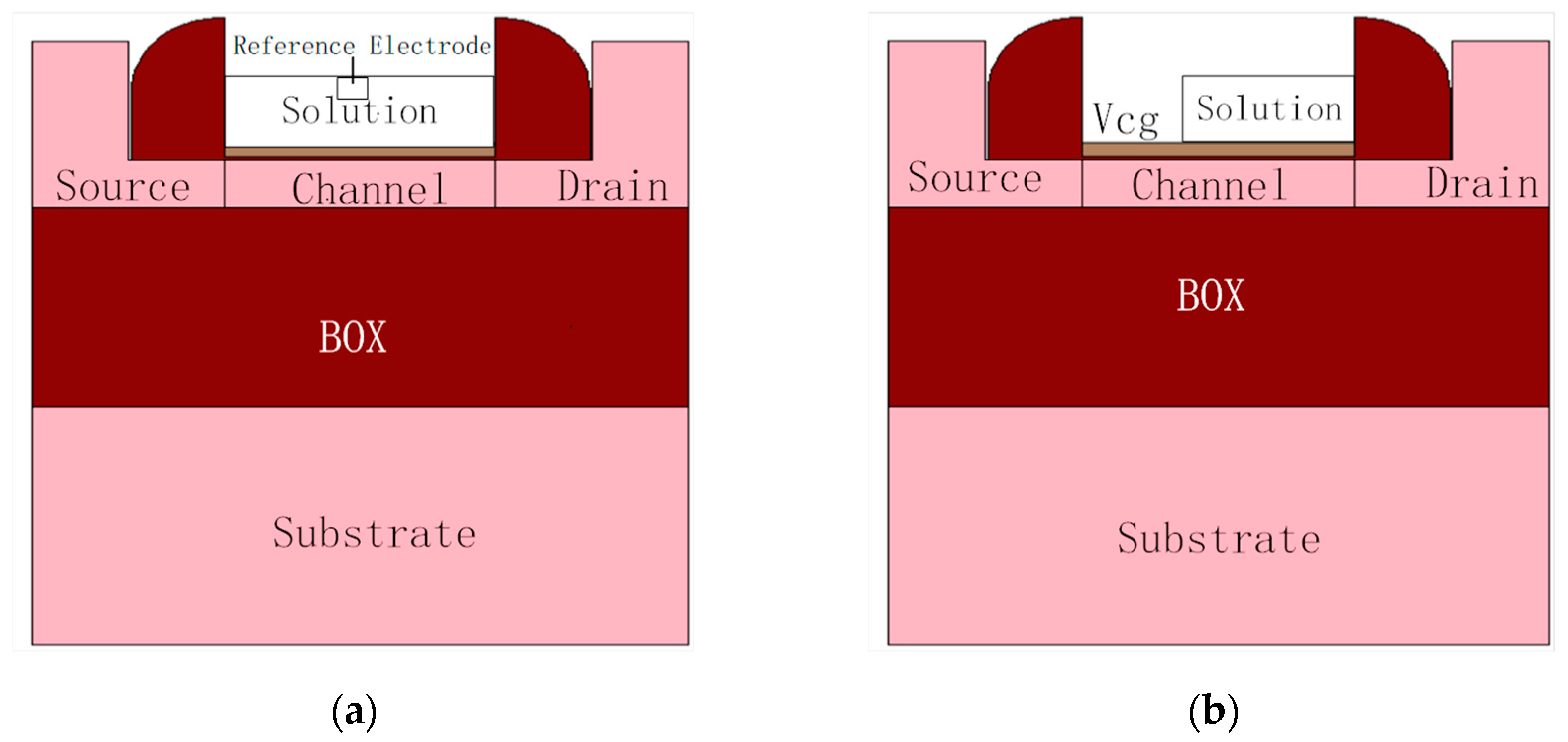
2.1. Devices and Models

Both single- and dual-gate FDSOI-ISFETs are based on 100 nm n-type FDSOI with an undoped channel, which is shown in Figure 1a. The structure of dual-gate FDSOI-ISFET is shown schematically in Figure 1b; the right half of the channel is set as a sensitive area for contact with the solution to be measured. The control gate voltage is applied to the left half of the channel, the reference voltage is set as 0 V and other physical parameters are shown in Table 1. The device models are established by using the Synopsys Sentaurus Device tool [21].
During the simulation, there are two challenges. One is determining how to define the solution under different pH conditions. In the simulation, the electrolyte is described as intrinsic silicon [3,22] in which the conduction band and the valence band are calculated [3,23]. The parameters such as carrier mobility and permittivity are modified to the corresponding values of water. The charge distribution in the solution is described by the Poisson–Boltzmann equation to simulate an electrical double layer [24]. The Poisson–Boltzmann equation can be described as (1) [24]
2 φ x 2 =   q ε { c 0 + e   q φ k B T   c 0 e q φ k B T } ,
where x is the distance from the surface of the solution to a specific point described, φ is the potential in the solution, q is the elementary charge, ε is the permittivity of water, c0+ and c 0 are the concentrations of cation and anion in the solution, kB is the Boltzmann constant and T is the temperature.
Another challenge is determining how to deal with the quantum confinement effects (QCEs). As the top silicon layer is only 6 nm, the QCEs have strong influences. According to previous research, QCEs will affect the threshold voltage and effective mobility of carriers in a thin layer [25,26]. In this way, the device cannot be described accurately using the classical transport model, so it is necessary to use a quantization model to describe the carrier’s transportation in the device. There are five different quantization models that can be used to describe QCEs under different situations. To balance both the speed and the accuracy of simulation [27,28], we choose the density gradient quantization model as the quantum correction model.

2.2. FDSOI ISFET Principle

There is a strong electrostatic coupling between the front gate and the back gate in FDSOI devices. When there is a change of front gate voltage, an amplified voltage shift of the back gate can be observed. The ratio of the change with the front gate and the back gate is defined as the coupling factor (γ) which is given by Equation (2) below. The relationship between ΔVbg and ΔVfg can be deduced as (3)
γ = Δ V bg Δ V fg = C ox C BOX ,
Δ V bg = C ox C BOX Δ V fg ,
where ΔVfg is the change of the front gate, ΔVbg is the voltage shift of the back gate, Cox is the capacitance of gate oxide and CBOX is the capacitance of buried oxide. The coupling factor γ can be adjusted by changing the thickness of the buried oxide while the thickness of the gate oxide is kept constant. According to the theoretical calculation, the γ value varies linearly with different thicknesses of the buried oxide layer. Figure 2a shows the variation of γ value with different thicknesses of the buried oxide layer (TBOX), confirming the mathematical model in Equation (2).
Figure 2b illustrates the ID-Vbg characteristics of the FDSOI device, as the front gate voltage increased from −200 mV to 200 mV with 25 nm TBOX. The fitting results prove the mathematical model of Equation (3).
As described in [17], the relationship between the proton concentration on the surface and the bulk of solution is described by Equation (4):
[ H + ] S = [ H + ] B exp ( q φ k B T ) ,
where [H+]S is the proton concentration on the surface of the solution and [H+]B is the proton concentration in the bulk of the solution.
The pH of the solution is determined by [H+]B and can be described by Equation (5):
pH = 10 log [ H + ] B ,
φ can be derived from Equation (4) as Equation (6):
φ = k B T q ln ( [ H + ] B [ H + ] S ) ,
For FDSOI-ISFETs, the changes in pH value introduce a change in the front gate potential, resulting in a shift of the back gate voltage. When the pH of the solution changes by dpH, a potential shift of dφ is presented at the front gate. The ratio can be expressed as the Nernst limit. The value of the Nernst limit is given by Equation (7):
d φ dpH = 2 . 3   ( k B T q )   α ,
where q is the elementary charge and α is the proton buffer capacity (0 ˂ α ˂ 1). This value is usually considered to be 59.6 mV/pH at room temperature.

3. Results and Discussion

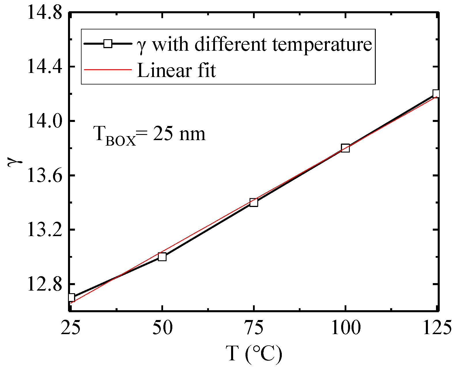
3.1. Influence of Temperature

The electrical characteristics and the sensitivity of the device at different operating temperatures were investigated. The corresponding γ values were calculated and are shown in Figure 3. The γ increases linearly with temperature from 25 to 125 ℃.
For choosing a more general case for solution measurement, the pH measurement sensitivity is discussed under 25 and 75 °C. As is shown in Figure 4a,c, at 25 °C (T = 25 °C), a voltage shift of 1.27 V can be seen at the back gate for every 100 mV change at the front gate, which means that the device has a maximum sensitivity of 12.7 times the Nernst limit (about 757 mV/pH), which is proved in Figure 4c. As is shown in Figure 4b, at 75 °C (T = 75 °C), the Nernst limit will change to 69.6 mV/pH according to (3); ΔVbg can reach 1.34V for every 100mV change at the front gate, and this gives a maximum sensitivity of 13.4 times the Nernst limit (about 933 mV/pH) theoretically. However, as is shown in Figure 4d, the sensitivity can only reach a maximum of 890 mV/pH (nearly 12.8 times the Nernst limit), which is somewhat attenuated compared to the theoretical value, but still increases about 140 mV/pH in sensitivity compared to the situation at 25 °C.

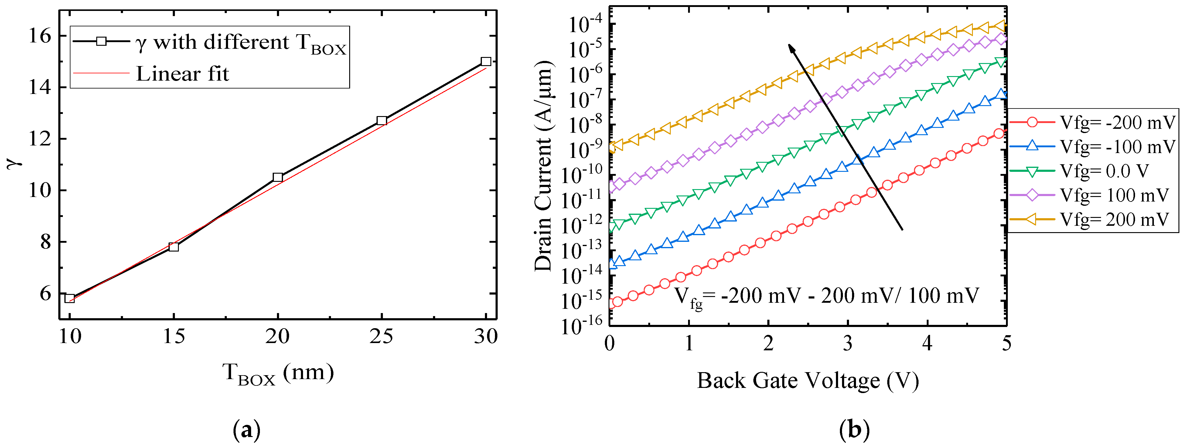
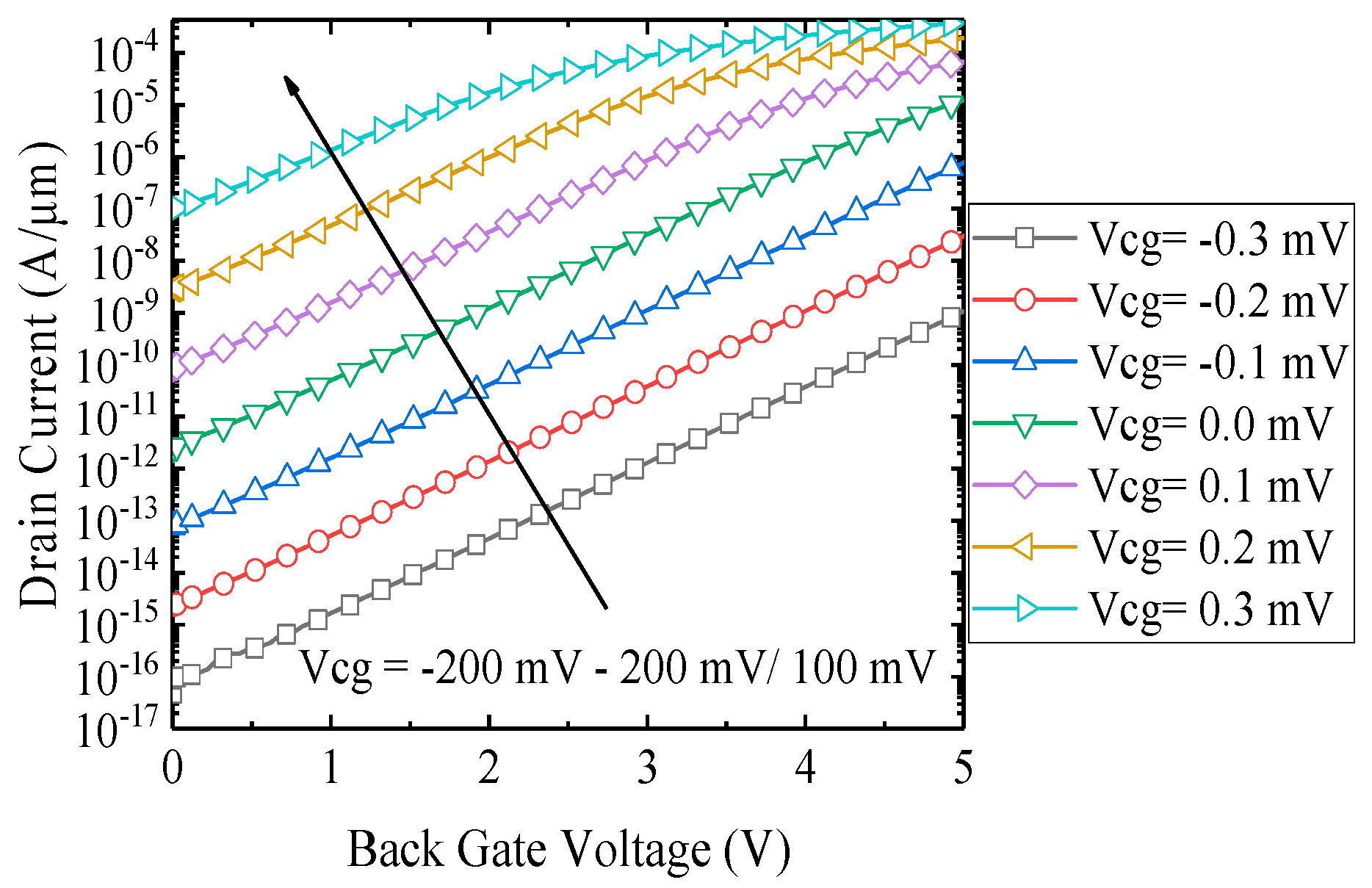
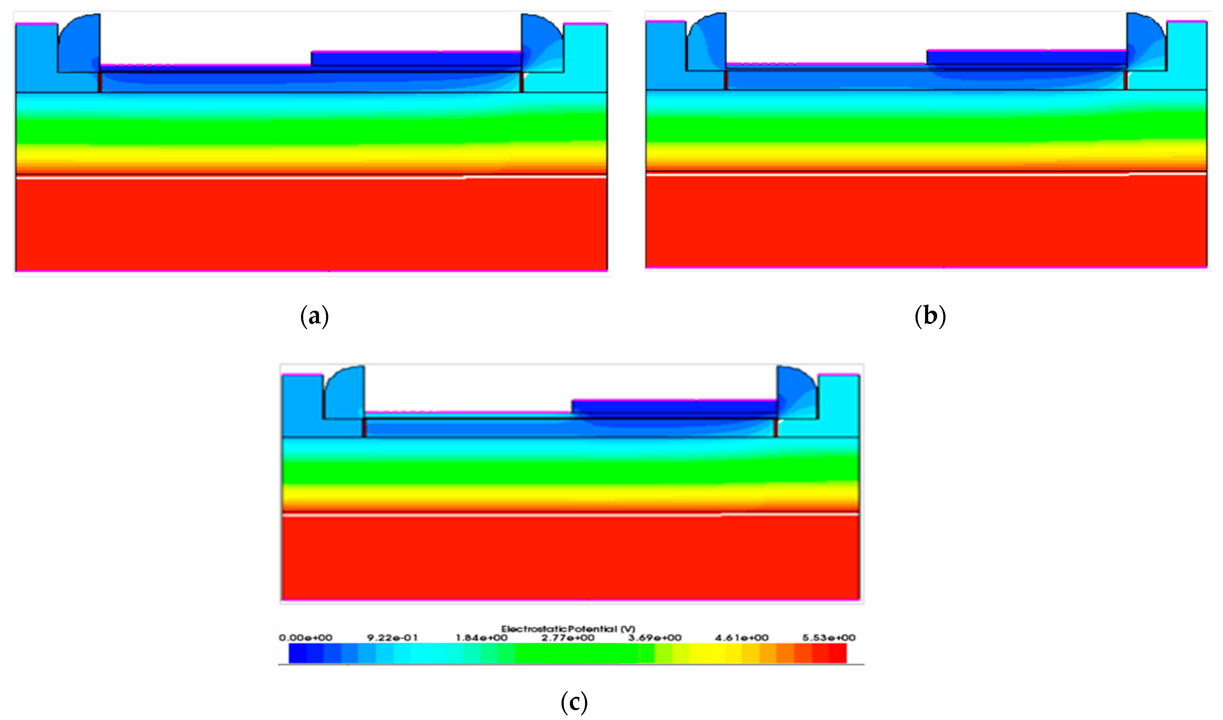
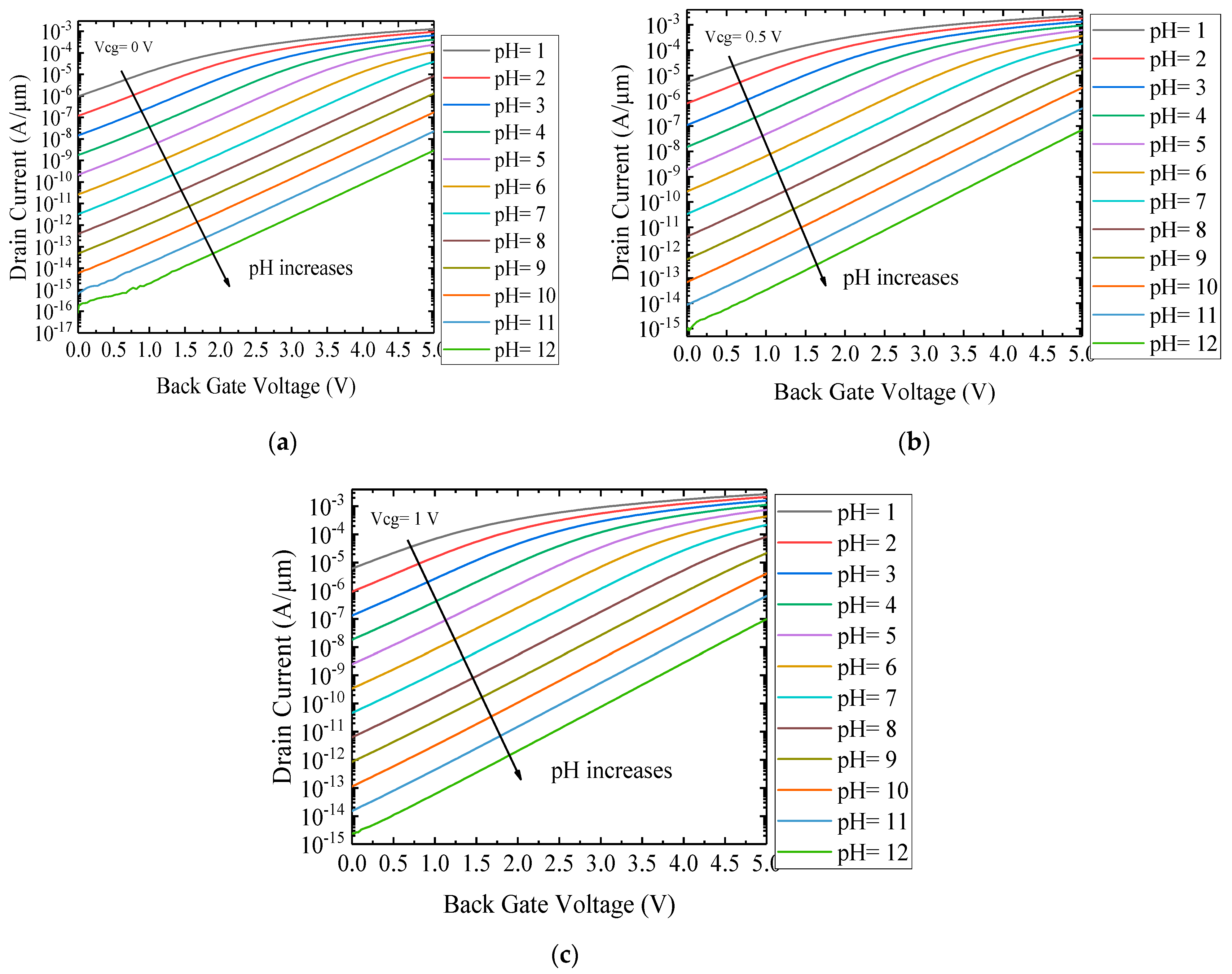
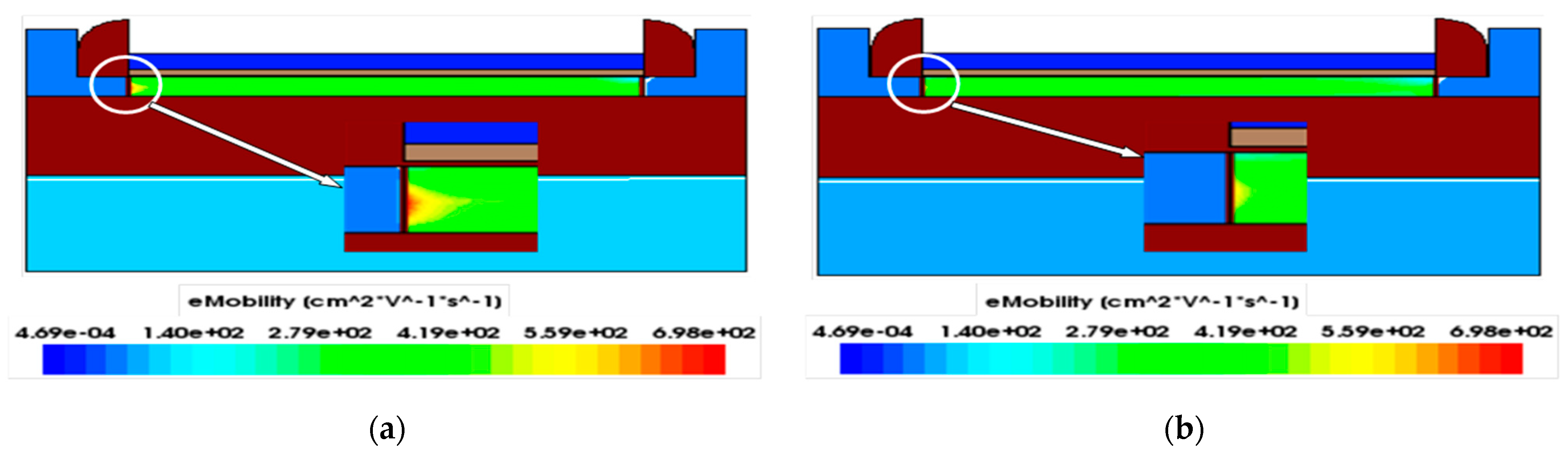
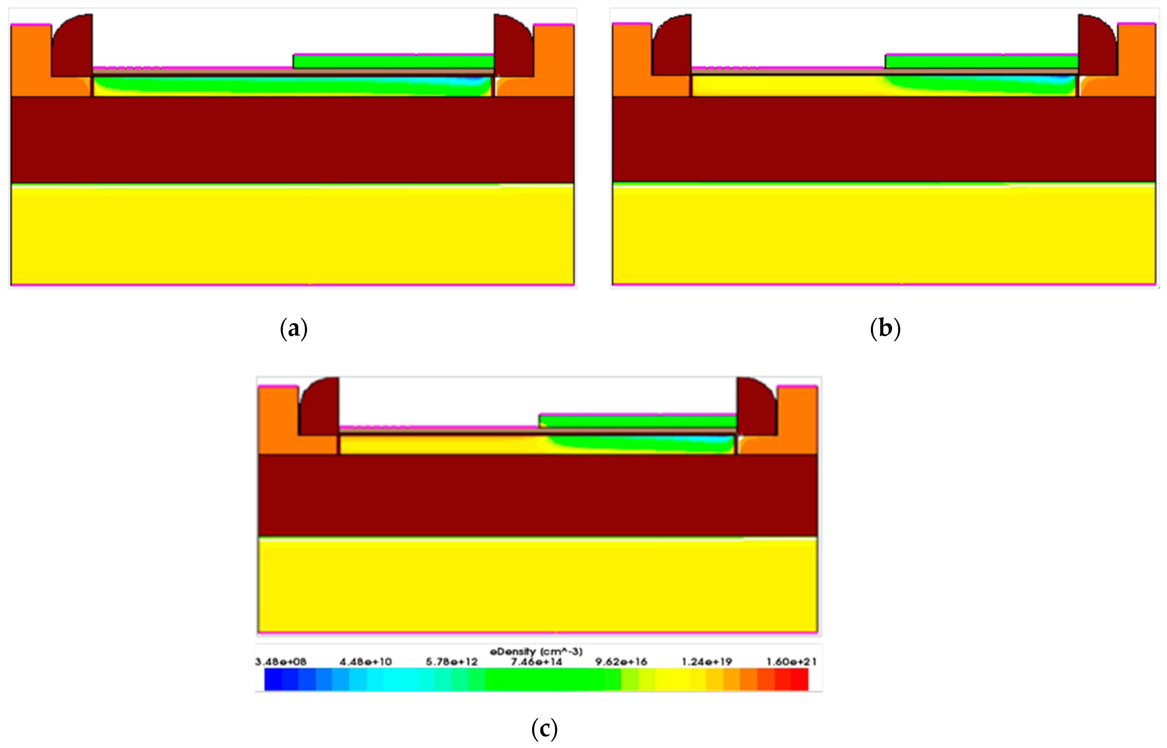
3.2. Influence of Dual-Gate Structure

The electrical characteristics and the sensitivity of the dual-gate FDSOI-ISFET under room temperature were obtained by simulation. The ID-Vbg curves with different control gate voltages (Vcg) are shown in Figure 5, from which the γ value of dual-gate FDSOI is 12.7, which is correspondent to the single-gate FDSOI discussed in Section 3.1.
The ID-Vbg curves of the device under different pH values are shown in Figure 6, while Vcg of Figure 6a, b and c is 0, 0.5 and 1 V respectively. When Vcg increases, the sensitivity of the device decreases gradually.
As is shown in Figure 6a, when Vcg = 0 V, the device has the maximum sensitivity of 750 mV/pH (12.5 times the Nernst limit under room temperature), and this is almost the same as the single-gate FDSOI-ISFET. When Vcg = 0.5 V, which is shown in Figure 6b, the sensitivity of the device drops to 624 mV/pH (10.4 times the Nernst limit under room temperature). When Vcg = 1V, which is shown in Figure 6c, the sensitivity of the device drops to 540 mV/pH (9 times the Nernst limit under room temperature).

3.3. Discussion

In practical application, the pH value is calculated through the change of threshold voltage, which is calculated through the change of drain current. Therefore, theoretically, changing the sensitivity of the device is actually modulating the change of the current. There are two ways to change the current in a semiconductor: changing the carrier mobility and changing the number of carriers.
For the single-gate FDSOI-ISFET, according to Equation (7), the absolute value of the Nernst limit increases with the increase of temperature, the coupling factor γ does not change, so the sensitivity value of the device increases. Although the carrier mobility decreases as the temperature increases, as shown in Figure 7, the result is the change of threshold voltage rather than the sensitivity [20].
The absolute value of the Nernst limit increases with the increase of temperature, the coupling factor γ does not change, so the sensitivity value of the device increases. Although the carrier mobility decreases as the temperature increases, as shown in Figure 7, the result is the change of threshold voltage rather than the sensitivity [20].
For the dual-gate FDSOI-ISFET, when the solution pH is 7, the electrostatic potential and the electron density of the device under different Vcg are shown in Figure 8 and Figure 9, respectively.
When the control gate voltage is the same as the reference voltage as 0 V, there is no electric field induced by the applied voltage, the sensitivity reaches the maximum.
However, when Vcg gradually rises, the electron density and electrostatic potential are affected by the control gate. As shown in Figure 8, the electrostatic potential under the control gate rises when Vcg rises. Because of the difference of the potential under the control gate and the solution, there is an electric field generated in the middle of the channel with a direction from control gate to the side of the solution. Therefore, the carriers move under the influence of the electric field. The electrons generated by the change of pH were supposed to move directly in the channel covered by solution, but they are concentrated near the side of the control gate under the affection of the electric field, which is shown in Figure 9. In this way, the number of electrons that should transfer the electric signal produced by pH change decreases, which leads to the decrease in sensitivity.
In summary, when Vcg increases, there is a potential difference between the control gate and solution, which leads to the generation of the electric field, causing carriers to move with the electric field to the side of the control gate. In this way, the influence of pH change of solution decreases and so does the sensitivity of the device.
Therefore, changing temperature is an effective way to change the sensitivity of a single-gate FDSOI-ISFET, because the sensitivity can be easily controlled by using the dual-gate structure. Since the sensitivity can be changed only by changing Vcg during use, the dual-gate structure may be used to obtain a FDSOI-ISFET with tunable sensitivity. However, it should be noted that the maximum sensitivity is still determined by γ, and changing Vcg can only reduce the sensitivity.

4. Conclusions

This work investigates the effects of temperature and dual-gate structure on the sensitivity of FDSOI-ISFET. By using a planar dual-gate structure, the sensitivity of a single FDSOI-ISFET on the chip can be adjusted independently by changing the control gate voltage rather than adjusting the back-gate voltage, which may infect the whole chip. The simulation revealed that the increase in operating temperature could enhance the sensitivity of the device. From 25 to 75 °C, the sensitivity increased by about 140 mV/pH. The electrical performance of the FDSOI using the dual gate is the same as that of the FDSOI using the single gate. Although the maximum sensitivity is determined by one factor of the FDSOI itself, the coupling factor γ, the sensitivity can be reduced by about 210 mV/pH by making Vcg greater than the reference voltage so that the device can be applied to a wide range of pH measurement.
This work provides guidance for obtaining FDSOI-ISFETs with adjustable sensitivity. The appropriate working temperatures and device structures can be chosen to obtain the devices suitable for their measuring sensitivity range.

Author Contributions

Funding acquisition, J.B.; methodology, J.B., M.L. and H.W.; software, J.B., M.L. and H.W.; investigation, J.B., M.L. and H.W.; resources, J.B., M.L. and H.W.; writing—original draft preparation, H.W.; writing—review and editing, J.B., M.L. and T.H.; supervision, J.B. and M.L.; All authors have read and agreed to the published version of the manuscript.

Funding

National Natural Science Foundation of China under Grant No. 61634008.

Acknowledgments

The software cited in this document is furnished under a license from Synopsis International Limited. Synopsis and Synopsis product names described herein are trademarks of Synopsis, Inc. The authors would like to thank all the participants in this study.

Conflicts of Interest

The authors declare no conflict of interest.

References

  1. Bergveld, P. Development, Operation, and Application of the Ion-Sensitive Field-Effect Transistor as a Tool for Electrophysiology. IEEE Trans. Biomed. Eng. 1972, 5, 342–351. [Google Scholar] [CrossRef] [PubMed]
  2. Moser, N.; Lande, T.S.; Toumazou, C.; Georgiou, P. ISFETs in CMOS and Emergent Trends in Instrumentation: A Review. IEEE Sens. J. 2016, 16, 6496–6514. [Google Scholar] [CrossRef]
  3. Passeri, D.; Morozzi, A.; Kanxheri, K.; Scorzoni, A. Numerical simulation of ISFET structures for biosensing devices with TCAD tools. Biomed. Eng. Online 2015, 14, 1–16. [Google Scholar] [CrossRef] [PubMed] [Green Version]
  4. Tarasov, A.; Wipf, M.; Stoop, R.L.; Bedner, K.; Fu, W.; Guzenko, V.A.; Knopfmacher, O.; Calame, M.; Schönenberger, C. Understanding the Electrolyte Background for Biochemical Sensing with Ion-Sensitive Field-Effect Transistors. ACS Nano 2012, 6, 9291. [Google Scholar] [CrossRef] [PubMed]
  5. Cheng, Q.; Wang, M.; Tao, M.; Yin, R.; Li, Y.; Yang, N.; Xu, W.; Gao, C.; Hao, Y.; Yang, Z. Planar Dual Gate GaN HEMT Cascode Amplifier as a Voltage Readout pH Sensor With High and Tunable Sensitivities. IEEE Electron Device Lett. 2020, 41, 485–488. [Google Scholar] [CrossRef]
  6. Li, Z.; Zhang, J.; Li, Y.; Shuang, Z.; Zhao, Y. Carbon Dots Based Photoelectrochemical Sensors for Ultrasensitive Detection of Glutathione and Its Applications in Probing of Myocardial Infarction. Biosensors Bioelectron. 2017, 99, 251. [Google Scholar] [CrossRef] [PubMed]
  7. Shuang, Z.A.; Cong, S.A.; Hha, B.; Zl, A.; Gang, X.A.; Qy, A.; Peng, S.A.; Lc, A.; Wn, A.; Jb, B. ISFET and Dex-AgNPs based portable sensor for reusable and real-time determinations of concanavalin A and glucose on smartphone. Biosensors Bioelectron. 2020, 151, 111962. [Google Scholar]
  8. Ayele, G.T.; Monfray, S.; Ecoffey, S.; Boeuf, F.; Cloarec, J.; Drouin, D.; Souifi, A. Ultrahigh-Sensitive CMOS pH Sensor Developed in the BEOL of Standard 28 nm UTBB FDSOI. IEEE J. Electron Devices Soc. 2018, 6, 1026–1032. [Google Scholar] [CrossRef]
  9. Wang, L.; Bu, Y.; Ao, J.-P. Effect of oxygen plasma treatment on the performance of AlGaN/GaN ion-sensitive field-effect transistors. Diam. Relat. Mater. 2017, 73, 1–6. [Google Scholar] [CrossRef]
  10. Yusof, K.A.; Noh, N.I.M.; Herman, S.H.; Abdullah, A.Z.; Zolkapli, M.; Abdullah, W.F.H. pH sensing characteristics of silicon nitride thin film and silicon nitride-based ISFET sensor. In Proceedings of the 2013 IEEE 4th Control and System Graduate Research Colloquium, Shah Alam, Malaysia, 19–20 August 2013; pp. 132–135. [Google Scholar]
  11. Chou, J.-C.; Weng, C.-Y.; Tsai, H.-M. Study on the temperature effects of Al2O3 gate pH-ISFET. Sens. Actuators B Chem. 2002, 81, 152–157. [Google Scholar] [CrossRef]
  12. Gimmel, P.; Schierbaum, K.D.; Göpel, W.; Vlekkert, H.; Rooij, N. Reduced light sensibility in optimized Ta2O5-ISFET structures. Sens. Actuators B Chem. 1991, 4, 135–140. [Google Scholar] [CrossRef]
  13. Poghossian, A.S. The super-Nernstian pH sensitivity of Ta2O5-gate ISFETs. Sens. Actuators B Chem. 1992, 7, 367–370. [Google Scholar] [CrossRef]
  14. Bausells, J.; Carrabina, J.; Errachid, A.; Merlos, A. Ion-sensitive field-effect transistors fabricated in a commercial CMOS technology. Sens. Actuators B Chem. 1999, 57, 56–62. [Google Scholar] [CrossRef] [Green Version]
  15. Rahhal, L.; Ayele, G.T.; Monfray, S.; Cloarec, J.-P.; Fornacciari, B.; Pardoux, E.; Chevalier, C.; Ecoffey, S.; Drouin, D.; Morin, P.; et al. High sensitivity pH sensing on the BEOL of industrial FDSOI transistors. Solid-State Electron. 2017, 134, 22–29. [Google Scholar] [CrossRef]
  16. Ayele, G.T.; Monfray, S.; Ecoffey, S.; Boeuf, F.; Bon, R.; Cloarec, J.P.; Drouin, D. Ultrahigh-Sensitive and CMOS Compatible ISFET Developed in BEOL of Industrial UTBB FDSOI. In Proceedings of the 2018 IEEE Symposium on VLSI Technology, Honolulu, HI, USA, 18–22 June 2018. [Google Scholar]
  17. Ayele, G.T.; Monfray, S.; Boeuf, F.; Cloarec, J.P.; Ecoffey, S.; Drouin, D.; Puyoo, E.; Souifi, A. Development of ultrasensitive extended-gate Ion-sensitive-field-effect-transistor based on industrial UTBB FDSOI transistor. In Proceedings of the 2017 47th European Solid-State Device Research Conference (ESSDERC), Leuven, Belgium, 11–14 September 2017; pp. 264–267. [Google Scholar]
  18. Pfattner, R.; Foudeh, A.M.; Chen, S.; Niu, W.; Matthews, J.R.; He, M.; Bao, Z. Dual-Gate Organic Field-Effect Transistor for pH Sensors with Tunable Sensitivity. Adv. Electron. Mater. 2019, 5, 1800381. [Google Scholar] [CrossRef] [Green Version]
  19. Son, T.; Le, S.C.; Curt, A. Richter, Arvind Balijepalli. Optimal field-effect transistor operation for high-resolution biochemical measurements. Rev. Sci. Instrum. 2021, 92, 030901. [Google Scholar]
  20. Dai, Y.; Huang, D.; Xing, J.; Pan, Z.; Zhang, B. Temperature Characteristics of an All-Solid-State Ion-Sensitive Field Effect Transistor pH Sensor. Semicond. Technol. 2018, 43, 734–739. [Google Scholar]
  21. Synopsys TCAD Tools. Available online: http://www.synopsys.com/Tools/TCADU (accessed on 25 January 2013).
  22. Mohammadi, E.; Manavizadeh, N. An Accurate TCAD-Based Model for ISFET Simulation. IEEE Trans. Electron Devices 2018, 65, 3950–3956. [Google Scholar] [CrossRef]
  23. Bandiziol, A.; Palestri, P.; Pittino, F.; Esseni, D.; Selmi, L. A TCAD-Based Methodology to Model the Site-Binding Charge at ISFET/Electrolyte Interfaces. IEEE Trans. Electron Devices 2015, 62, 3379–3386. [Google Scholar] [CrossRef]
  24. Chung, I.Y.; Jang, H.; Lee, J.; Moon, H.; Seo, S.M.; Kim, D.H. Simulation study on discrete charge effects of SiNW biosensors according to bound target position using a 3D TCAD simulator. Nanotechnology 2012, 23, 123–133. [Google Scholar] [CrossRef] [Green Version]
  25. Esseni, D.; Abramo, A.; Selmi, L.; Sangiorgi, E. Physically based modeling of low field electron mobility in ultrathin single- and double-gate SOI n-MOSFETs. IEEE Trans. Electron Devices 2003, 50, 2445–2455. [Google Scholar] [CrossRef]
  26. Poljak, M.; Jovanovic, V.; Grgec, D.; Suligoj, T. Assessment of Electron Mobility in Ultrathin-Body InGaAs-on-Insulator MOSFETs Using Physics-Based Modeling. IEEE Trans. Electron Devices 2012, 59, 1636–1643. [Google Scholar] [CrossRef]
  27. Lyumkis, E.; Mickevicius, R.; Penzin, O.; Polsky, B.; El Sayed, K.; Wettstein, A. Simulations of ultrathin SOI with quantum transport models. In Proceedings of the 2001 IEEE International SOI Conference, Durango, CO, USA, 1–4 October 2001; pp. 49–50. [Google Scholar]
  28. Poiroux, T.; Widiez, J.; Lolivier, J.; Vinet, M.; Casse, M.; Prévitali, B.; Deleonibus, S. New and accurate method for electrical extraction of silicon film thickness on fully-depleted SOI and double gate transistors. In Proceedings of the 2004 IEEE International SOI Conference (IEEE Cat. No.04CH37573), Charleston, SC, USA, 4–7 October 2004; pp. 73–74. [Google Scholar]
Figure 1. Illustrations of (a) 100 nm n-type FDSOI and (b) dual-gate FDSOI-ISFET.
Electronics 10 01585 g001
Figure 2. (a) Different γ values and the linear fitting curve with different TBOX; (b) ID-Vbg curves of FDSOI device with different front gate voltages.
Electronics 10 01585 g002
Figure 3. Different γ values and the linear fitting curve at different operating temperatures.
Electronics 10 01585 g003
Figure 4. ID-Vbg curves of single-gate FDSOI-ISFET under different temperatures and pH: (a) ID-Vbg curves at different front gate voltages when T = 25 °C; (b) ID-Vbg curves at different front gate voltages when T = 75 °C; (c) ID-Vbg curves at different pH when T = 25 °C; (d) ID-Vbg curves at different pH when T = 75 °C.
Electronics 10 01585 g004
Figure 5. ID-Vbg curves of dual-gate FDSOI-ISFET under different control gate voltages.
Electronics 10 01585 g005
Figure 6. ID-Vbg curves of the device under different pH values when (a) Vcg = 0 V, (b) Vcg = 0.5 V and (c) Vcg = 1 V.
Electronics 10 01585 g006
Figure 7. Electron mobility of the device when (a) T = 25 °C and (b) T = 75 °C.
Electronics 10 01585 g007
Figure 8. Electrostatic potential of the device when (a) Vcg = 0 V, (b) Vcg = 0.5 V and (c) Vcg = 1 V.
Electronics 10 01585 g008
Figure 9. Electron density of the device when (a) Vcg = 0 V, (b) Vcg = 0.5 V and (c) Vcg = 1 V.
Electronics 10 01585 g009
Table 1. Physical parameters of FDSOI-ISFET for TCAD simulations.
ParametersValues
Top Silicon Thickness6 nm
Buried Oxide Thickness25 nm
Length of Sensing Area50 nm
Doping Concentration of Source and Drain Area1 × 1020 cm−3
Publisher’s Note: MDPI stays neutral with regard to jurisdictional claims in published maps and institutional affiliations.

