Article

An Anti-Interference Online Monitoring Method for IGBT Bond Wire Aging

School of Electrical Engineering and Automation, Wuhan University, Wuhan 430072, China
*
Author to whom correspondence should be addressed.
Electronics 2021, 10(12), 1449; https://doi.org/10.3390/electronics10121449
Submission received: 13 May 2021 / Revised: 9 June 2021 / Accepted: 10 June 2021 / Published: 17 June 2021

Abstract

:
Due to the constant changes of the environment and load, the insulated-gate bipolar transistor (IGBT) module is subjected to a large amount of junction temperature (Tj) fluctuations, which often leads to damage to the bond wires. The monitoring parameters of IGBTs are often coupled with Tj, which increases the difficulty of monitoring IGBTs’ health status online. In this paper, based on the collector current (Ic) and collector-emitter on-state voltage (Vce_on) online monitoring circuit, an online monitoring method of IGBT bond wire aging against interference is proposed. First, the bond wire aging model is established, and the Vce_on is selected as the monitoring parameter. Secondly, taking a three-phase inverter circuit as an example, the Vce_on and Ic waveforms of the IGBT module are monitored in real time, and the process of online monitoring is introduced accordingly. Finally, the experimental results output by RT-LAB indicate that the method proposed in this paper can accurately identify the aging state of IGBT bond wires under different conditions.

1. Introduction

Compared with other power electronic devices, the insulated-gate bipolar transistor (IGBT) power module has many advantages, such as large input impedance, small driving power, a simple control circuit, small switching loss, and high working frequency, so it has been widely used in power converters [1,2]. In recent years, the application of power converters has been expanding, such as in wind power generation, solar power generation, electric vehicles, and aerospace power systems [3,4,5,6], which have harsh operating conditions and strict requirements for IGBT reliability. According to the reliability survey report of the converter system, the power semiconductor device is the component with the highest failure rate in the converter system, accounting for about 34% of failures [7].
Due to the complex and changeable working conditions of the power converter, the IGBT is subjected to a large number of thermal stress, overvoltage, and overcurrent impacts in the process of operation [8,9]. Bond wire aging and solder layer aging are the two most common fatigue failure types of IGBT modules. On account of the different coefficients of thermal expansion (CTE) of the module materials, the thermal stress of the internal structure is uneven under temperature fluctuations, which eventually leads to damage to the bond wires and the solder layer [10,11,12]. The IGBT module can continue to operate for a period of time before complete failure. Therefore, if potential variations due to aging can be detected before complete failure, catastrophic failure can be avoided. In practical applications, the fatigue failure of IGBT modules is mostly manifested as the bond wires completely lift off [13,14]. IGBT bond wire aging monitoring is very necessary to improve the reliability of the converter, which is also the focus of this paper. Owing to the hindrance of the package structure of the IGBT module, it is difficult to directly monitor the aging process of bond wires. When the bond wire is broken, the equivalent parameters of the emitter area will change so that the external electrical parameters of the IGBT module will also change accordingly, which provides the possibility for condition monitoring. Therefore, some external electrical parameters with significant variations can be regarded as monitoring parameters for evaluating IGBT aging.
The existing monitoring parameters can be divided into the following categories:
  • Current-based parameter: short-circuit current (Is). In [15], the authors took the Is as the monitoring parameter for bond wire aging. When the number of broken bond wires in the IGBT module gradually increases, the Is will decrease accordingly. However, this method needs to inject current into the IGBT module, which is not suitable for online monitoring application scenarios.
  • Time-based parameter: turn-on time (ton) and turn-off time (toff). The authors in [16,17] calculated ton by measuring the current and voltage waveforms during IGBT turn-on and monitor bond wire failures accordingly. The experimental results show that the ton under the bond wire failure was shorter than that under the healthy state. In [18], the charging time of the gate capacitance was measured by injecting a small current during the IGBT turn-off period to monitor the health status of the bond wires. Since the switching time of the IGBT was in the range of 10–500 ns, the time-based parameters had extremely high requirements for the hardware measurement circuit.
  • Voltage-based parameter: gate voltage (Vg) and collector-emitter on-state voltage (Vce_on). In [19], the Vge was used to monitor the multi-chip parallel IGBT modules’ health status. The experimental results showed that this method would not be affected by load current changes or noise caused by switching. However, only when all bond wires of a specific IGBT chip were broken did the Vge change significantly. The application of this method was limited to multi-chip parallel IGBT modules, which are not universal. The authors of [20,21] cut the bond wire to simulate IGBT aging and monitor the IGBT health status by measuring Vce_on online. The results indicated that Vce_on could accurately identify the number of broken bond wires.
  • Temperature-based parameter: junction temperature (Tj) and thermal resistance (Rth). In [22], the case temperature (Tc) and junction temperature (Tj) were observed by thermocouples to calculate the Rth. When the Rth increased by 20%, the IGBT module failed. However, this method needs to invade the IGBT module package for measurement, which is not conducive to online monitoring. In [23], Tj was obtained by measuring the linear relationship between Vce_on and Tj, whereas in [24], Tj was calculated by the turn-off overshoot voltage. It is worth noting that Tj cannot directly reflect the aging state of the IGBT, but it has a close coupling relationship with other parameters, which are called thermosensitive electrical parameters (TSEPs) [25,26]. Almost all the above monitoring parameters for bond wire are TSEPs.
Considering online monitoring capabilities, hardware cost, and measurement accuracy, Vce_on is most suitable for monitoring the aging state of bond wires [27]. Although Vce_on is very suitable as the IGBT monitoring parameter, the voltage between the collector and the emitter can be hundreds of times different when the IGBT is turned on and off at high speed, making it difficult to sample Vce_on online and accurately. In [28], a sampling circuit based on the IGBT, current source, and voltage source is proposed. By modifying the converter’s PWM control signal, different currents are injected into the converter during the window period to obtain Vce_on. Although this sampling circuit can realize the online monitoring of the IGBT, it has a significant influence on the converter’s working state. In [29], a sampling circuit based on the current source, diode, and MOSFET is proposed which indirectly measures Vce_on by measuring the voltage at the test point. When the IGBT is on, the test point voltage is the sum of the diode conduction voltage drop, the resistance voltage drop, and the Vce_on. When the IGBT is off, the MOSFET is turned on to shield the high voltage between the collector and the emitter. This sampling circuit also needs to inject current into the test circuit and indirectly measure the Vce_on. All in all, the existing Vce_on sampling circuit needs to inject current into the converter or modify the control signal, which will not affect the working state of the converter to varying degrees.
While Vce_on has a strong correlation with bond wire aging, it also has a coupling relationship with Tj. During the operation of the photovoltaic, wind power, and new energy vehicles, Tj of the IGBT module changes all the time, which will interfere with the judgment of the bond wires’ aging state. The existing method eliminates the interference of Tj by injecting current into the IGBT module [23,30], which will not be suitable for online monitoring. The authors of [31] calculated the equivalent resistance at the bonding area based on the offline measurement of Vce_on and evaluated the health status of the independent IGBT module accordingly. Although this method considers the influence of Tj, it belongs to the field of IGBT offline reliability evaluation and does not provide a solution for online monitoring under actual working conditions. In general, the existing online monitoring methods are difficult for effectively eliminating the interference of Tj.
Motivated by the analysis described above, based on the voltage and current sampling circuit, this paper proposes an online monitoring method for the IGBT bond wire against Tj interference. The method proposed in this paper can non-intrusively monitor IGBT modules online, which can reduce unnecessary downtime for maintenance. The innovation of the sampling circuit is that it can obtain the full-period waveform of Vce_on varying with the collector current (Ic) during the modulation period. The circuit cleverly utilizes the current flowing through the IGBT and the corresponding turn-on voltage drop during the IGBT working process, and it does not need to inject additional current into the circuit or modify the control signal to collect aging parameters. It obtains the intersection collector current (Iint) such that Vce_on is not disturbed by Tj via the IGBT bond wire aging model and datasheet. Then, it compares the real-time sampling waveforms of Ic and Vce_on to obtain the collector-emitter on-state voltage corresponding to Iint (Vce_int). Finally, the bond wire aging state can be judged based on Vce_int, which is not interfered with by Tj.
This paper is organized as follows. Section 2 establishes the aging model of the IGBT bond wire and selects the Vce_int value as the aging parameter in combination with the datasheet. Section 3 illustrates the working principle of the sampling circuit and introduces the online monitoring process based on the sampling waveform. Section 4 takes a three-phase inverter as an example for experimental verification and uses the method proposed in this paper to monitor the bond wire aging under the interference of DC voltage and Tj. Section 5 draws the conclusions.

2. IGBT Bond Wire Aging Modeling

2.1. Bond Wire Aging Mechanism

The basic internal structure of the IGBT module is shown in Figure 1a. To meet the rated current requirements and improve the performance, the IGBT module is usually composed of multiple IGBT chips in parallel, in which the emitter and gate of the chip and the corresponding terminals need to be connected via bond wires. Due to the large CTE difference between aluminum and silicon materials, the thermal stress on the chip and the bond wire under the action of the temperature field is inconsistent, causing shear stress at the bonding area of the bond wire and the chip [32], which can be expressed as
ε = (α1α2)·ΔT
where α1 and α2 are the CTE of the bond wire and the silicon chip, ΔT represents the temperature fluctuation, and L is the length of the bonding area between the bond wire and the silicon chip.
In the actual working process of the IGBT, the continuous thermal stress impact makes the bonding area age, and the specific manifestation is the bond wire’s lift-off. As long as one of the bond wires in the IGBT module breaks first, the current passing through the remaining bond wires will increase and bear greater thermal stress impact, which will accelerate the failure of the IGBT device. Therefore, bond wire lift-off is one of the main modes of IGBT failure in practical engineering applications.

2.2. Bond Wire Aging Model

Since the Vce_on of the IGBT module is affected by both aging and Tj, it is necessary to exclude the influence of Tj on the Vce_on to accurately reflect the bond wire aging. In the actual operation of converters, it is difficult to accurately control and measure the internal Tj of the IGBT module, which makes it harder to determine whether the variation in the Vce_on is caused by Tj or aging.
Taking the FF50R12RT4 half-bridge module as an example, the IGBT in the module contain six bond wires, as shown in Figure 1b. Vce_on is affected by Tj and Ic in a healthy state [28], as shown in Equation (2):
Vce_on = V0 − k1·(Tj− Tj0) + [R0 + k2·(Tj − Tj0)]·Ic
where V0 and R0 are the on-state voltage and on-state resistance of the IGBT at the reference junction temperature Tj0, respectively, and k1 and k2 are the temperature coefficients of V0 and R0, respectively.
When the IGBT bond wires are broken due to thermal stress impact, R0 will change, which will affect Vce_on. The equation of Vce_on under the bond wire aging is as follows:
Vce_on = V0k1·(TjTj0)+ [R0 + ΔR + k2·(TjTj0)]·Ic
where ΔR represents the variation in the on-state resistance of the IGBT caused by the broken bond wire and k1·(Tj − Tj0) is inversely proportional to (TjTj0), whereas [R0 + ΔR + k2·(Tj − Tj0)]·Ic is directly proportional to (TjTj0). The contribution of the former is negative, while the contribution of the latter is positive. There is a value Iint, where Vce_on is not affected by the Tj. When Ic = Iint, Vce_on at this time is called Vce_int, as shown in Equation (4), where k1·(Tj − Tj0) and k2·(Tj − Tj0Ic cancel each other out and Vce_int is only affected by (R0 + ΔRIc:
Vce_int = V0− k1·(Tj− Tj0) + (R0 + ΔRIc + k2·(Tj − Tj0Ic
Therefore, Vce_int can accurately reflect the voltage drop change caused by the bond wire aging and is not affected by Tj, which can be regarded as the monitoring parameter of bond wire aging.
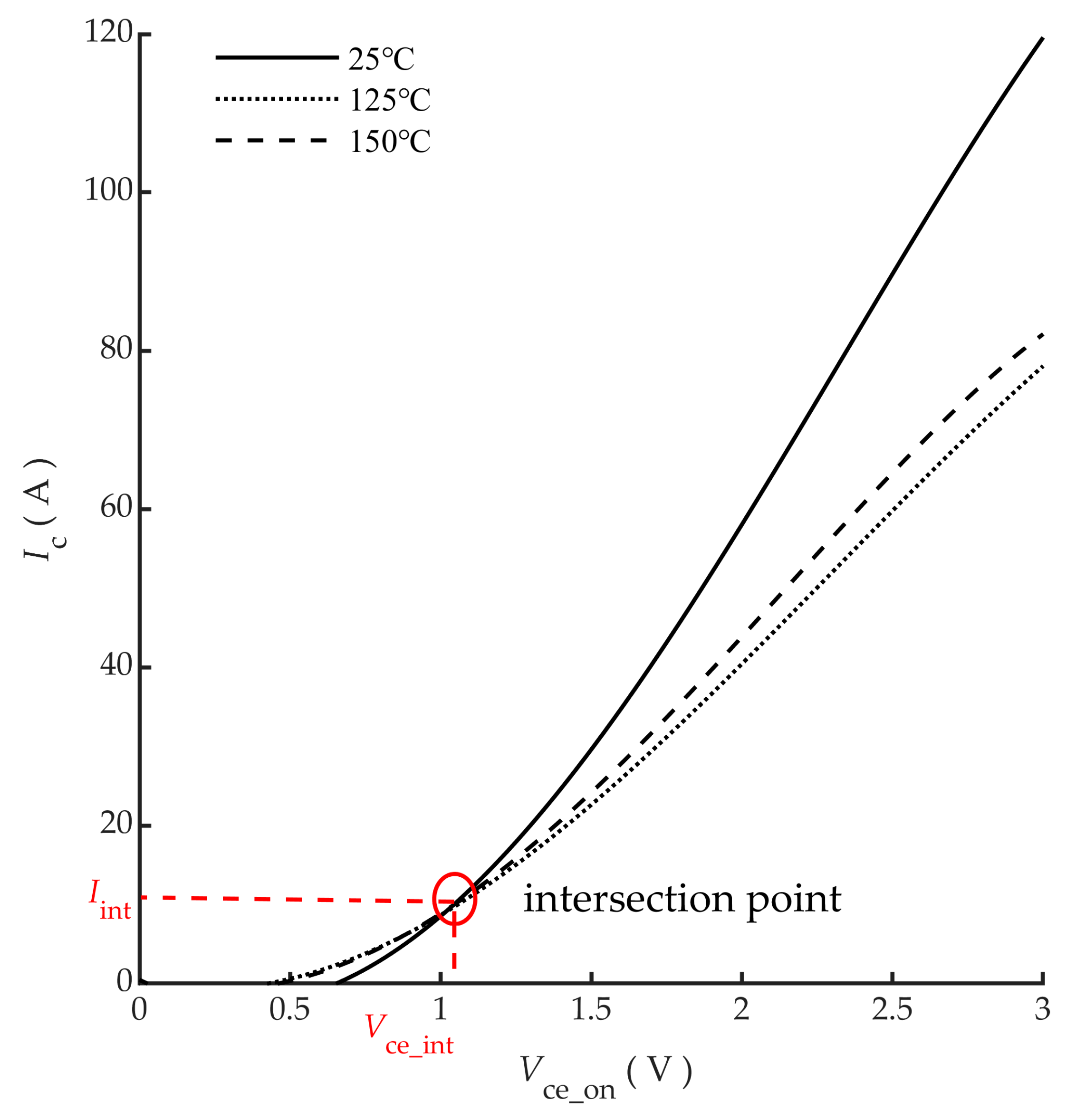
Referring to the datasheet of the FF50R12RT4 IGBT module, the typical values of Iint and Vce_int can be obtained according to their output characteristic curves, as shown in Figure 2. When Tj is 25 °C, 125 °C or 150 °C, the output characteristic curve of the IGBT module will have an intersection where Iint = 12 A. When Ic = Iint, Vce_int is not affected by Tj, which is consistent with the previous discussion.

3. Online Monitoring of IGBT Bond Wire Aging

In this paper, a three-phase inverter is taken as an example to illustrate the working principle of the proposed anti-interference online monitoring method for bond wire aging. It will be explained in two parts: the sampling circuit and online monitoring.

3.1. Sampling Circuit

Although Vce_on is very suitable as an IGBT aging parameter, the voltage between the collector and the emitter can be hundreds of times different when the IGBT is turned on and off at a high speed, making it difficult to sample Vce_on online and accurately. The Vce_on sampling circuit utilized in this paper was implemented in three steps: clamping, filtering, and amplifying, as presented in Figure 3. Clamping refers to the high-voltage shielding between the collector and emitter during the turn-off period of the IGBT via the switching of two MOSFETs (M1 and M2). Take the U-phase upper leg IGBT (S1) as an example to explain the working principle. When S1 is turned on, M1 is turned on so that the voltage sampling channel is turned on, thereby sampling Vce_on. When S1 is turned off, M2 is turned on, so the voltage sampling channel is clamped to the ground potential, thereby shielding the high voltage between collector and emitter. The specific control diagram is shown in Table 1.
Filtering is related to eliminating the noise contained in the waveform obtained after clamping by a second-order RC circuit, but it also produces a certain degree of attenuation. Amplification refers to the use of an operational amplifier to compensate for the waveform attenuation caused by the filter part, which ensures the accuracy of the sampled waveform. As for the current sampling part, Hall current sensors are used for synchronous sampling. The voltage and current waveforms obtained by the sampling circuit are presented in Figure 3. By comparing the waveforms, Iint and Vint can be further collected to prepare for condition monitoring.

3.2. Online Monitoring

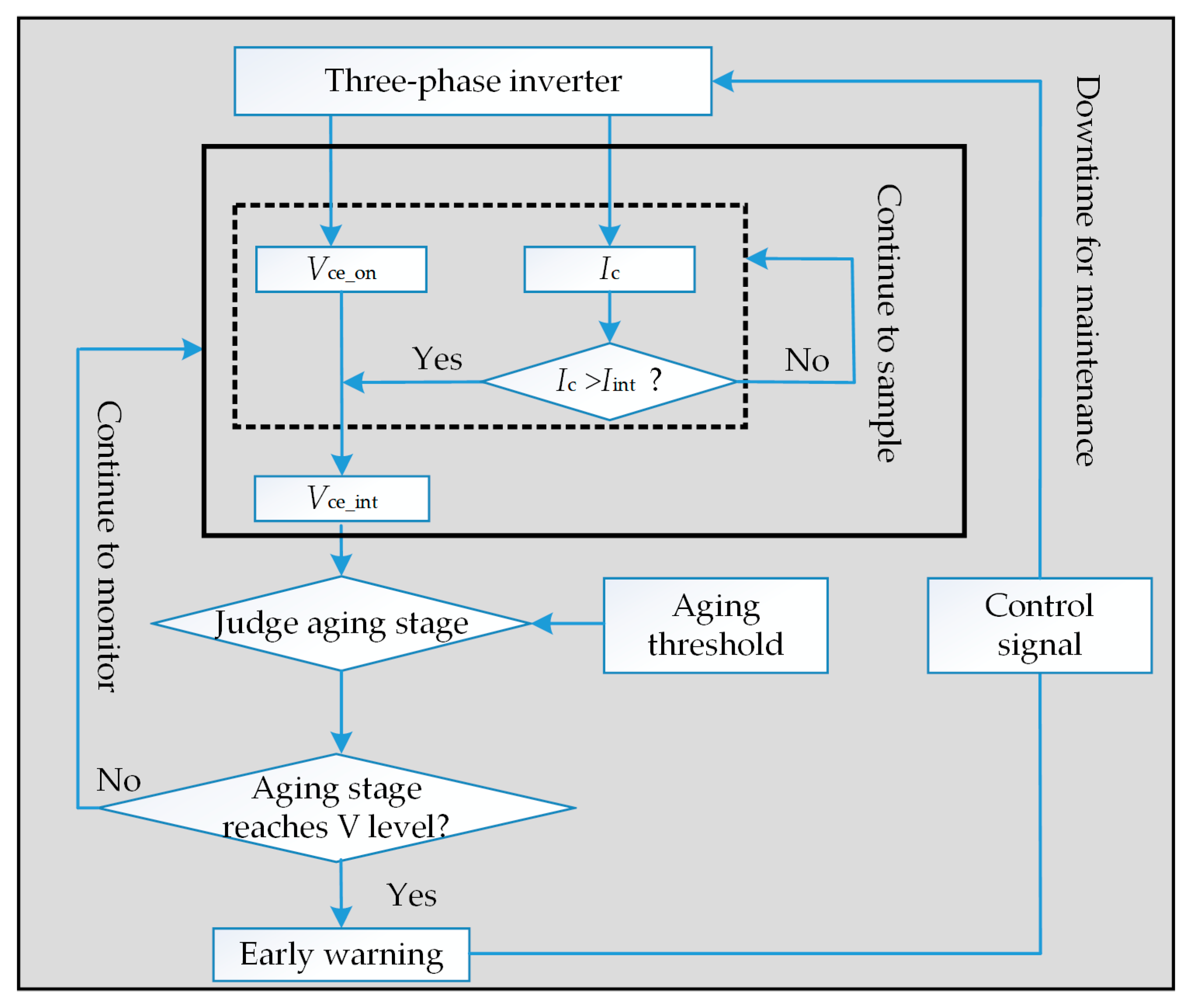
Based on the above sampling circuit, this paper proposes an online monitoring method for IGBT bond wire aging, as illustrated in Figure 4. First, the voltage and current sampling circuits are used to collect the Vce_on and Ic waveforms of the three-phase inverter system in real time. Second, considering the impact of fluctuations on the DC side or the load side on Ic, the amplitude of Ic is compared with that of Iint. Only when the amplitude of Ic is greater than Iint is the corresponding Vce_int sampling performed. Then, Vce_int is compared with the aging threshold to judge the aging state of the bond wires. Finally, when the aging state reaches the failure threshold set in advance, a failure warning is triggered to the control system. The measurement of the aging threshold will be described in detail in the next section.

4. Experiment and Result Analysis

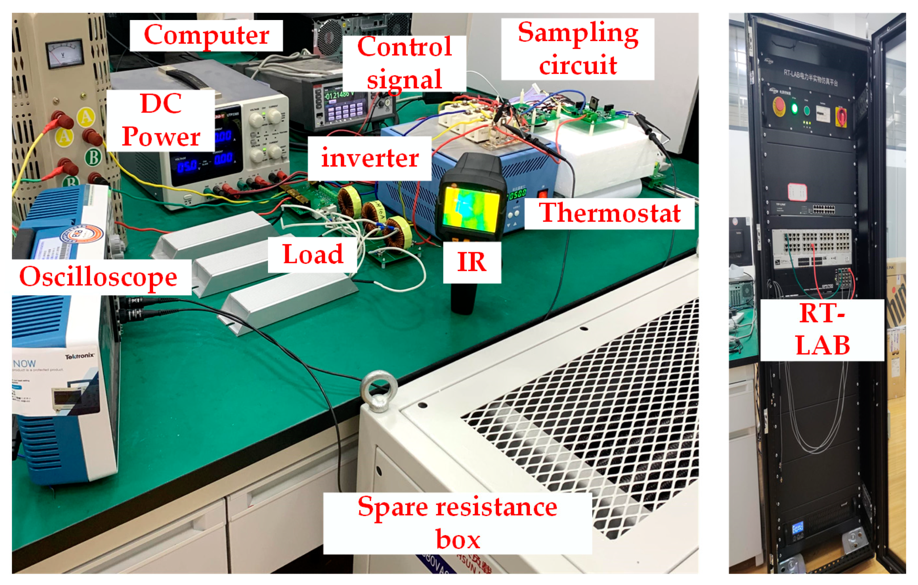
In order to verify the effectiveness of the method proposed in this paper, an experimental platform for aging monitoring was built as presented in Figure 5, which included the DC power supply, three-phase inverter circuit, sampling circuit, thermostat, IR thermal imager, and control unit. The experimental parameter settings are listed in Table 2. It is worth noting that the voltage and current signals collected in this paper were input into RT-LAB for high-precision A/D conversion.

4.1. Sampling under DC Voltage Fluctuations

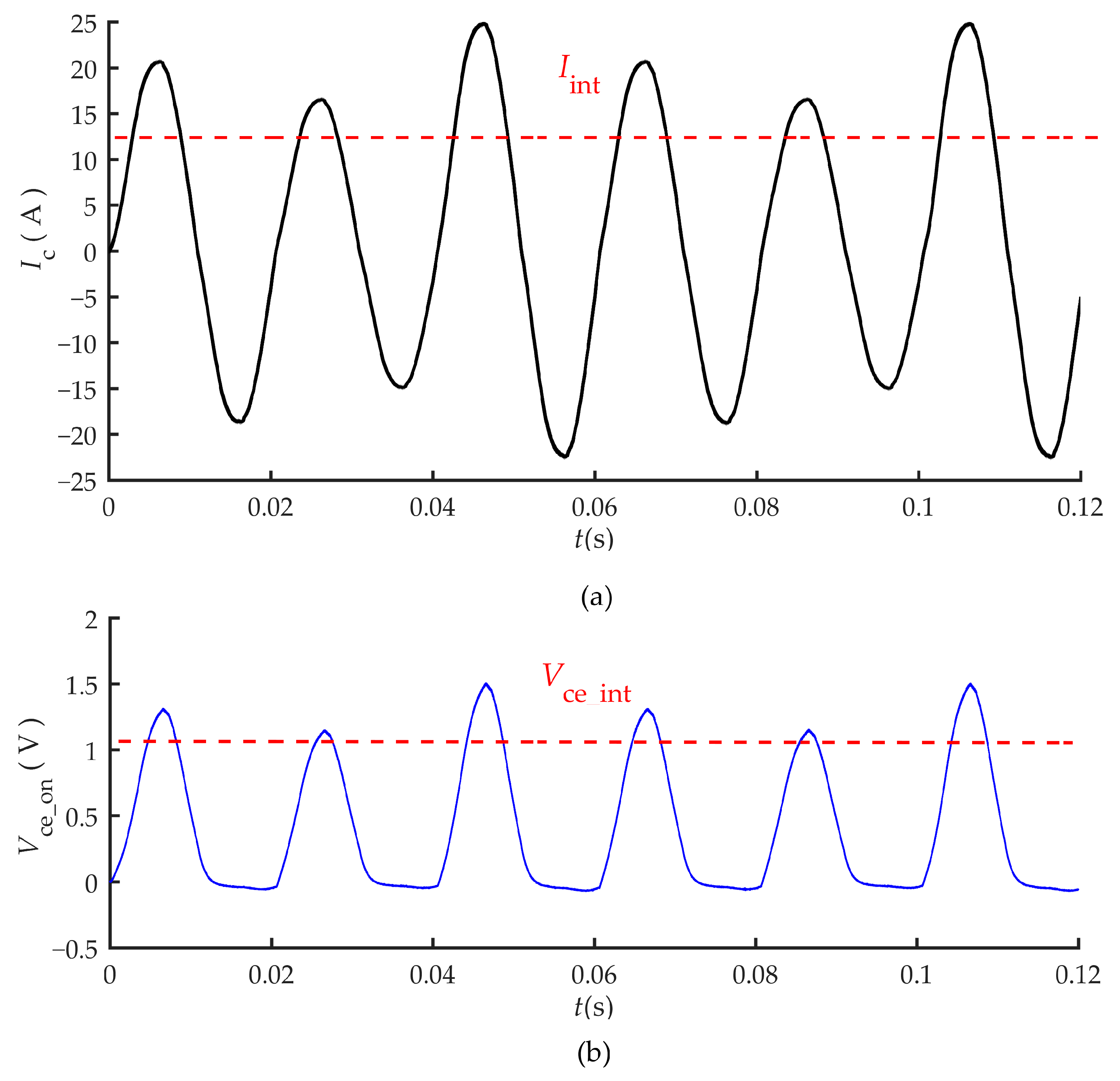
In the actual working process of the inverter, it will be subjected to electrical disturbances on the load or DC voltage side, which will cause Ic fluctuations. In order to prove that the sampling circuit could still maintain excellent working performance under this disturbance, this paper carried out relevant sampling under the condition of DC voltage fluctuation, as shown in Figure 6. It could be found that the Vce_on waveform could follow the fluctuation of Ic, which indicates that the sampling circuit had good anti-interference performance. The red dotted line marks Iint and its corresponding Vint, which are the basis for subsequent condition monitoring.
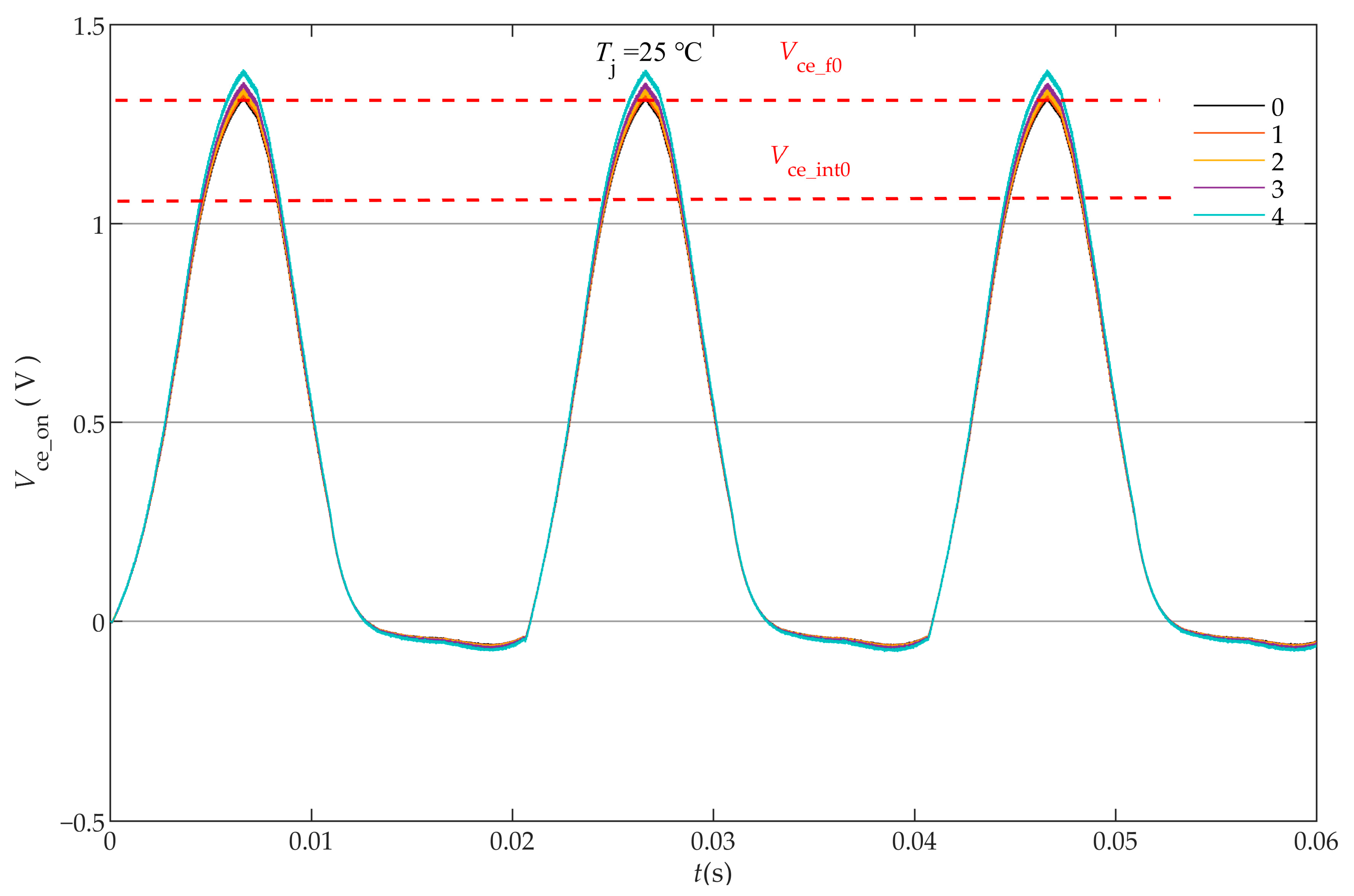
In the case of Tj = 25 °C, Vce_int was selected when the IGBT was fully healthy (Vce_int0) as the healthy reference value. When 1–4 bond wires were broken (see Figure 7), the corresponding Vce_int was sampled, and Equation (5) was used to calculate the deviation percentage of each aging stage (ΔVce_int), which was regarded as the aging indicator, as listed in Table 2. For subsequent comparison, this paper also measured the Vce_on amplitude voltage (Vce_f0) in the healthy state and calculated the deviation percentage of each aging stage (ΔVce_f) according to Equation (6), as listed in Table 3. The two dashed lines marked in Figure 7 are the health reference values. After measurement, Vce_int0 and Vce_f0 could be obtained as 1.05 V and 1.32 V, respectively:
ΔVce_int = (Vce_intVce_int0)/Vce_int0
ΔVce_f = (Vce_fVce_f0)/Vce_f0

4.2. Junction Temperature Interference

Taking three bond wires’ lift-off as an example to illustrate the interference of Tj, the Tj of S1 was stabilized at 50 °C and 75 °C by adjusting the thermostat to simulate Tj fluctuations. In the above four cases, the Vce_on waveform is shown in Figure 8. It can be found that the waveform near Vce_int was not affected by Tj. Vce_int did not deviate with the increase in Tj, which could accurately reflect the aging state of the bond wires. In addition, the waveform near Vce_f was most disturbed by Tj. Vce_f had a significant deviation as Vce_f increased, and the maximum deviation reached 60 mV. In summary, selecting Vce as the aging indicator could achieve resistance to the interference of Tj.

4.3. Aging Monitoring Results

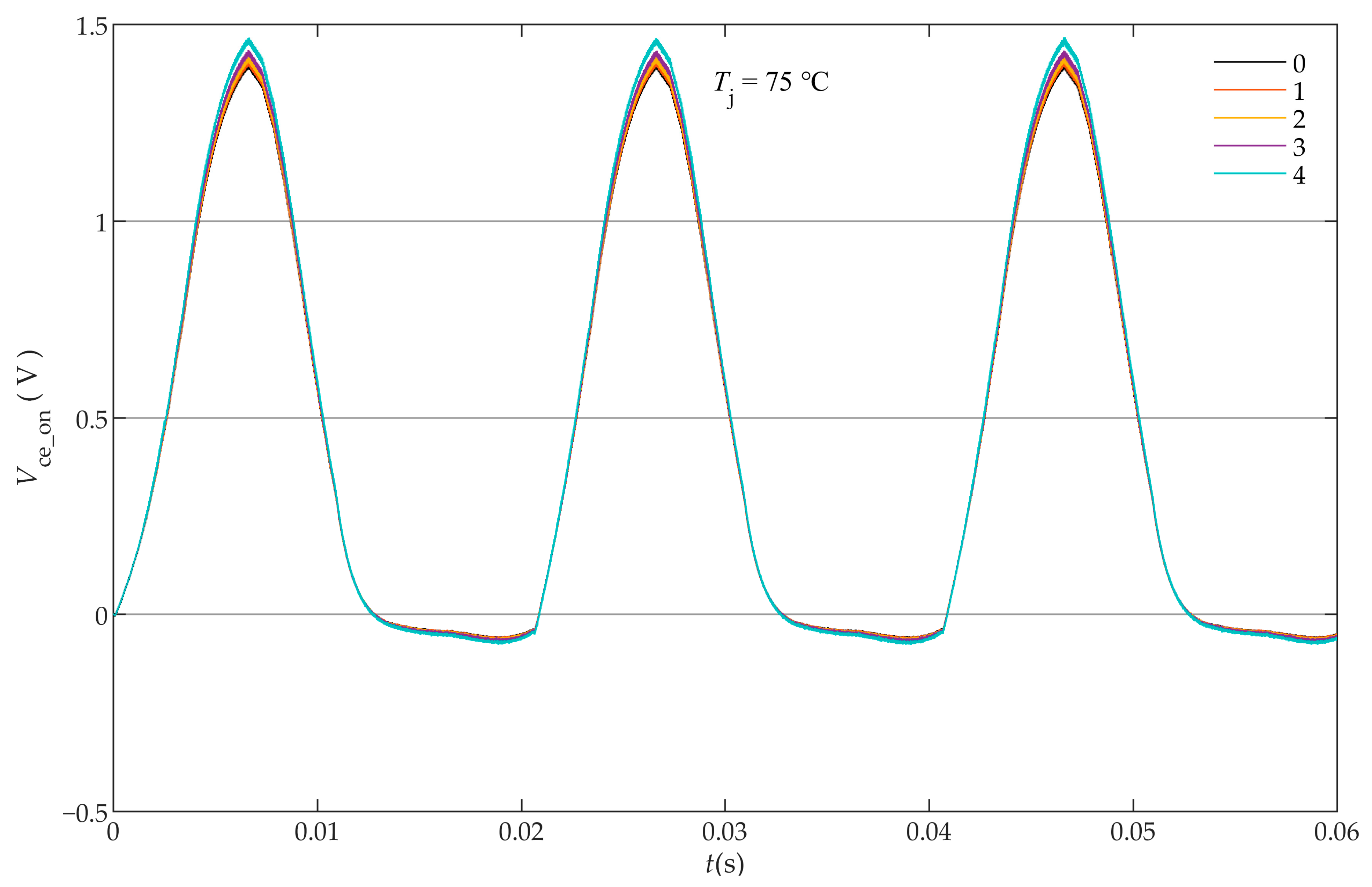
In order to show that the monitoring method proposed in this paper could eliminate the interference of Tj, in the case of Tj = 75 °C, the sampling circuit was used to measure Vce_on under different bond wire aging stages, as shown in Figure 9. Using Equations (5) and (6), the aging index of each aging stage was calculated. The aging indicators with the previously determined aging threshold (see Table 3) were compared to judge the current aging state, as shown in Table 4.
When Tj rose from 25 °C to 75 °C, Vce_int had a slight deviation compared with Vce_int0, but ΔVce_int could still accurately reflect the current aging state. On the contrary, Vce_f had a large deviation compared with Vce_f0, and ΔVce_f was far away from the current aging state. For example, when the IGBT was in aging stage II, ΔVce_int was 0.86%, which was judged as aging state I according to the aging thresholds. However, ΔVce_f was 6.21%, which was misjudged as aging stage V.
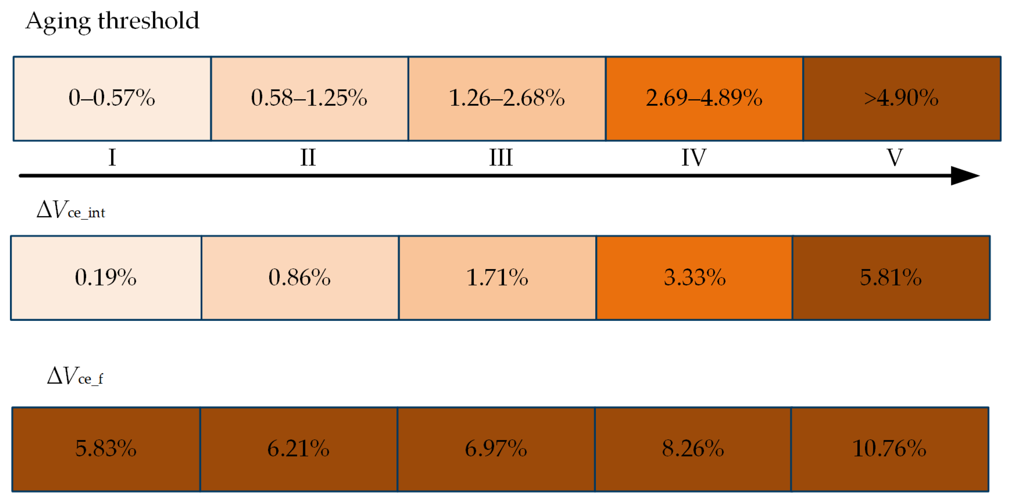
In order to compare the aging monitoring results more intuitively, different color blocks in Figure 10 are used to indicate the different aging stages. It can be clearly seen that the monitoring results based on ΔVce_int could accurately distinguish each aging stage, while the monitoring results based on ΔVce_f deviated far from the actual situation. In general, Vce_int had good resistance to the interference of Tj. For this three-phase inverter system, when the monitoring circuit detected that the aging indicator exceeded 4.90%, the aging state of the IGBT bond wire was judged as stage V. At this time, a shutdown maintenance signal was triggered in the control system.

5. Conclusions

The aging parameter Vce_int, which is not affected by Tj, is obtained by combining the IGBT aging model and the datasheet. Moreover, Vce_int is collected in real time to judge the aging state of the IGBT bond wire by comparing the Ic and Vce_on waveforms. Different from the existing method, this method cleverly utilizes the current flowing through the IGBT and the corresponding turn-on voltage drop during the IGBT working process, and it does not need to inject additional current into the circuit or modify the control signal to collect the aging parameters. In addition, the anti-interference online monitoring method proposed in this paper can reduce downtime for maintenance.
The experimental results output by RT-LAB prove that the method proposed in this paper can judge the aging state of the IGBT bond wire in the three-phase inverter under the condition of DC voltage disturbance and junction temperature disturbance. It is worth noting that this paper only introduced this method’s application in a three-phase inverter system, and it also applies to other power electronic converters.

Author Contributions

Conceptualization, methodology, software, validation, formal analysis, investigation, and resources, C.W. and Y.H.; data curation, writing—original draft preparation, Y.J.; writing—review and editing and visualization, L.L. All authors have read and agreed to the published version of the manuscript.

Funding

This research was funded by the National Natural Science Foundation of China (Grant No. 51977153, 51977161, 51577046), the Fundamental Research Funds for the Central Universities of China (Grant No. 2042021kf0233), the State Key Program of the National Natural Science Foundation of China (Grant No. 51637004), the national key research and development plan “important scientific instruments and equipment development” of China (Grant No. 2016YFF0102200), “smart grid technology and equipment” of China (Grant No. 2020YFB0905905), the Equipment Research Project in Advance of China (Grant No. 41402040301), and the Wuhan Science and Technology Plan Project (Grant No. 20201G01).

Conflicts of Interest

The authors declare no conflict of interest.

References

  1. Choi, U.-M.; Blaabjerg, F.; Lee, K.-B. Study and Handling Methods of Power IGBT Module Failures in Power Electronic Converter Systems. IEEE Trans. Power Electron. 2015, 30, 2517–2533. [Google Scholar] [CrossRef]
  2. Li, H.; Liao, X.; Zeng, Z.; Hu, Y.; Li, Y.; Liu, S.; Ran, L. Thermal Coupling Analysis in a Multichip Paralleled IGBT Module for a DFIG Wind Turbine Power Converter. IEEE Trans. Energy Convers. 2016, 32, 80–90. [Google Scholar] [CrossRef] [Green Version]
  3. Lai, W.; Wang, Z.; Hu, Y.; Chen, M.; Xia, H.; Luo, D.; Wei, Y.; Gao, B.; Chen, Y. Evaluation of IGBT Module Remaining Lifetime in Wind Power Converters Considering Impacts of Failure Location. IEEE Trans. Electron Devices 2021, 68, 1810–1818. [Google Scholar] [CrossRef]
  4. Reigosa, P.D.; Wang, H.; Yang, Y.; Blaabjerg, F. Prediction of Bond Wire Fatigue of IGBTs in a PV Inverter under a Long-Term Operation. IEEE Trans. Power Electron. 2015, 31, 7171–7182. [Google Scholar] [CrossRef] [Green Version]
  5. Ji, B.; Song, X.; Cao, W.; Pickert, V.; Hu, Y.; Mackersie, J.W.; Pierce, G. In Situ Diagnostics and Prognostics of Solder Fatigue in IGBT Modules for Electric Vehicle Drives. IEEE Trans. Power Electron. 2015, 30, 1535–1543. [Google Scholar] [CrossRef]
  6. Buticchi, G.; Barater, D.; Costa, L.F.; Liserre, M. A PV-Inspired Low-Common-Mode Dual-Active-Bridge Converter for Aerospace Applications. IEEE Trans. Power Electron. 2018, 33, 10467–10477. [Google Scholar] [CrossRef] [Green Version]
  7. Yang, S.; Xiang, D.; Bryant, A.; Mawby, P.; Ran, L.; Tavner, P. Condition Monitoring for Device Reliability in Power Electronic Converters: A Review. IEEE Trans. Power Electron. 2010, 25, 2734–2752. [Google Scholar] [CrossRef]
  8. Oh, H.; Han, B.; McCluskey, P.; Han, C.; Youn, B.D. Physics-of-Failure, Condition Monitoring, and Prognostics of Insulated Gate Bipolar Transistor Modules: A Review. IEEE Trans. Power Electron. 2015, 30, 2413–2426. [Google Scholar] [CrossRef]
  9. Abuelnaga, A.; Narimani, M.; Bahman, A.S. A Review on IGBT Module Failure Modes and Lifetime Testing. IEEE Access. 2021, 9, 9643–9663. [Google Scholar] [CrossRef]
  10. Hu, K.; Liu, Z.; Yang, Y.; Iannuzzo, F.; Blaabjerg, F. Ensuring a Reliable Operation of Two-Level IGBT-Based Power Converters: A Review of Monitoring and Fault-Tolerant Approaches. IEEE Access. 2020, 8, 89988–90022. [Google Scholar] [CrossRef]
  11. Wang, H.; Liserre, M.; Blaabjerg, F.; Rimmen, P.D.P.; Jacobsen, J.B.; Kvisgaard, T.; Landkildehus, J. Transitioning to Physics-of-Failure as a Reliability Driver in Power Electronics. IEEE J. Emerg. Sel. Top. Power Electron. 2014, 2, 97–114. [Google Scholar] [CrossRef]
  12. Sabbah, W.; Arabi, F.; Avino-Salvado, O.; Buttay, C.; Théolier, L.; Morel, H. Lifetime of power electronics interconnections in accelerated test conditions: High temperature storage and thermal cycling. Microelectron. Reliab. 2017, 76–77, 444–449. [Google Scholar] [CrossRef] [Green Version]
  13. Hanif, A.; Devoto, D.; Khan, F.H. Bond Wire Damage Detection and SOH Estimation of a Dual-Pack IGBT Power Module Using Active Power Cycling and Reflectometry. IEEE Trans. Power Electron. 2019, 35, 6761–6772. [Google Scholar] [CrossRef]
  14. Gonzalez-Hernando, F.; San-Sebastian, J.; Garcia-Bediaga, A.; Arias, M.; Iannuzzo, F.; Blaabjerg, F. Wear-Out Condition Monitoring of IGBT and mosfet Power Modules in Inverter Operation. IEEE Trans. Ind. Appl. 2019, 55, 6184–6192. [Google Scholar] [CrossRef]
  15. Sun, P.; Gong, C.; Du, X.; Peng, Y.; Wang, B.; Zhou, L. Condition Monitoring IGBT Module Bond Wires Fatigue Using Short-Circuit Current Identification. IEEE Trans. Power Electron. 2016, 32, 3777–3786. [Google Scholar] [CrossRef]
  16. Zhou, L.; Zhou, S.; Xu, M. Investigation of gate voltage oscillations in an IGBT module after partial bond wires lift-off. Microelectron. Reliab. 2013, 53, 282–287. [Google Scholar] [CrossRef]
  17. Zhou, S.; Zhou, L.; Sun, P. Monitoring Potential Defects in an IGBT Module Based on Dynamic Changes of the Gate Current. IEEE Trans. Power Electron. 2013, 28, 1479–1487. [Google Scholar] [CrossRef]
  18. Wang, K.; Zhou, L.; Sun, P.; Du, X. Monitoring Bond Wires Fatigue of Multichip IGBT module Using Time Duration of The Gate Charge. IEEE Trans. Power Electron. 2020, 36, 888–897. [Google Scholar] [CrossRef]
  19. Mandeya, R.; Chen, C.; Pickert, V.; Naayagi, R.T.; Ji, B. Gate–Emitter Pre-threshold Voltage as a Health-Sensitive Parameter for IGBT Chip Failure Monitoring in High-Voltage Multichip IGBT Power Modules. IEEE Trans. Power Electron. 2018, 34, 9158–9169. [Google Scholar] [CrossRef] [Green Version]
  20. Choi, U.-M.; Blaabjerg, F.; Jorgensen, S.; Munk-Nielsen, S.; Rannestad, B. Reliability Improvement of Power Converters by Means of Condition Monitoring of IGBT Modules. IEEE Trans. Power Electron. 2017, 32, 7990–7997. [Google Scholar] [CrossRef]
  21. Choi, U.-M.; Blaabjerg, F. Separation of Wear-Out Failure Modes of IGBT Modules in Grid-Connected Inverter Systems. IEEE Trans. Power Electron. 2017, 33, 6217–6223. [Google Scholar] [CrossRef]
  22. Sathik, M.H.M.; Sundararajan, P.; Sasongko, F.; Pou, J.; Natarajan, S. Comparative Analysis of IGBT Parameters Variation Under Different Accelerated Aging Tests. IEEE Trans. Electron Devices 2020, 67, 1098–1105. [Google Scholar] [CrossRef]
  23. Wang, X.; Sun, P.; Sun, L.; Luo, Q.; Du, X. Online Condition Monitoring for Bond Wire Degradation of IGBT Modules in Three-Level Neutral-Point-Clamped Converters. IEEE Trans. Ind. Electron. 2021, 68, 7474–7484. [Google Scholar] [CrossRef]
  24. Yang, Y.; Zhang, P. In situ IGBT Junction Temperature Estimation Method via a Bond Wire Degradation Independent Parameter Turn-off Vce Overshoot. IEEE Trans. Ind. Electron. 2020, PP, 1. [Google Scholar] [CrossRef]
  25. Zhang, J.; Du, M.; Jing, L.; Wei, K.; Hurley, W.G. IGBT Junction Temperature Measurements: Inclusive of Dynamic Thermal Parameters. IEEE Trans. Device Mater. Reliab. 2019, 19, 333–340. [Google Scholar] [CrossRef]
  26. Avenas, Y.; Dupont, L.; Khatir, Z. Temperature Measurement of Power Semiconductor Devices by Thermo-Sensitive Electrical Parameters—A Review. IEEE Trans. Power Electron. 2012, 27, 3081–3092. [Google Scholar] [CrossRef] [Green Version]
  27. Fang, X.; Lin, S.; Huang, X.; Lin, F.; Yang, Z.; Igarashi, S. A review of data-driven prognostic for IGBT remaining useful life. Chin. J. Electr. Eng. 2018, 4, 73–79. [Google Scholar] [CrossRef]
  28. Ma, M.; Ji, B.; Han, J.; Zhan, M.; Xiang, N. In-situ health monitoring of IGBT modules of an on-line medium-voltage inverter system using for industrial Internet of Things. CSEE J. Power Energy Syst. 2020, 6, 638–648. [Google Scholar] [CrossRef]
  29. Yang, Y.; Zhang, Q.; Zhang, P. A Fast IGBT Junction Temperature Estimation Approach Based on ON-State Voltage Drop. IEEE Trans. Ind. Appl. 2021, 57, 685–693. [Google Scholar] [CrossRef]
  30. Ji, B.; Pickert, V.; Cao, W.; Zahawi, B. In Situ Diagnostics and Prognostics of Wire Bonding Faults in IGBT Modules for Electric Vehicle Drives. IEEE Trans. Power Electron. 2013, 28, 5568–5577. [Google Scholar] [CrossRef] [Green Version]
  31. He, Y. IGBT Module Reliability Evaluation Method and Device Based on Bonding Lead Degradation. C.N. Patent 111,856,233B, 27 April 2021. [Google Scholar]
  32. Ciappa, M. Selected failure mechanisms of modern power modules. Microelectron. Reliab. 2002, 42, 653–667. [Google Scholar] [CrossRef]
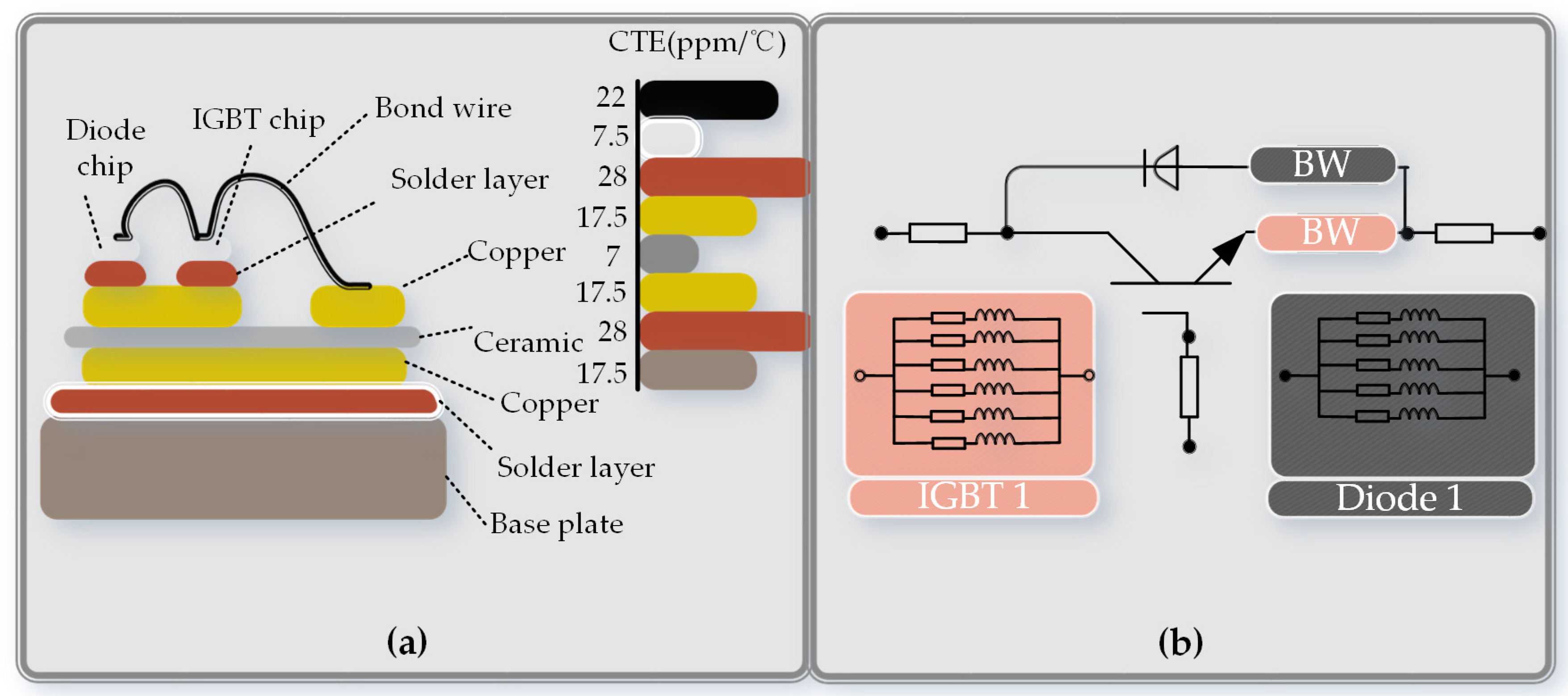
Figure 1. (a) The structure of the IGBT (insulated-gate bipolar transistor) module. (b) Equivalent model of the IGBT bond wires.
Electronics 10 01449 g001
Figure 2. IGBT output characteristic curve.
Electronics 10 01449 g002
Figure 3. Working principle of the voltage and current sampling circuit.
Electronics 10 01449 g003
Figure 4. Voltage and current sampling circuit.
Electronics 10 01449 g004
Figure 5. Aging monitoring platform.
Electronics 10 01449 g005
Figure 6. (a) The waveform of Ic. (b) The waveform of Vce_on.
Electronics 10 01449 g006
Figure 7. Online monitoring results with different broken bond wires in the case of Tj = 25 °C.
Electronics 10 01449 g007
Figure 8. Online monitoring results with different junction temperatures.
Electronics 10 01449 g008
Figure 9. Online monitoring results with different broken bond wires in the case of Tj = 75 °C.
Electronics 10 01449 g009
Figure 10. Comparison of aging monitoring results.
Electronics 10 01449 g010
Table 1. Voltage sampling circuit drive signal.
SwitchM1M2M3M4
S1 on1000
S1 off0100
S2 on0010
S2 off0001
Table 2. Experimental platform parameter settings.
ParametersValues
Switching frequency (fsw)20 kHz
Output frequency (f)50 Hz
IGBT module typeFF50R12RT4
IR typeTesto 865
Thermostat typeJF-966
Junction temperature (Tj)25–75 °C
Number of broken bond wires0–4
Resolution of ADC16-bit
Gain band width of amplifier4 MHz
Table 3. Aging threshold.
Number of Broken Bond WiresAging Threshold for Vce_intAging Threshold for Vce_fAging States
0<0.57%<0.68%I
10.58–1.25%0.69–1.14%II
21.26–2.68%1.15–2.58%III
32.69–4.89%2.59–4.86%VI
4>4.90%>4.86%V
Table 4. Aging monitoring results in the case of Tj = 75 °C.
Number of Broken Bond WiresVce_int (V)ΔVce_intVce_f (V)ΔVce_f
01.0520.19%, I1.3975.83%, V
11.0590.86%, II1.4026.21%, V
21.0681.71%, III1.4126.97%, V
31.0853.33%, IV1.4298.26%, V
41.1115.81%, V1.46210.76%, V
Publisher’s Note: MDPI stays neutral with regard to jurisdictional claims in published maps and institutional affiliations.