
A Novel Fast-Locking ADPLL Based on Bisection Method


Abstract
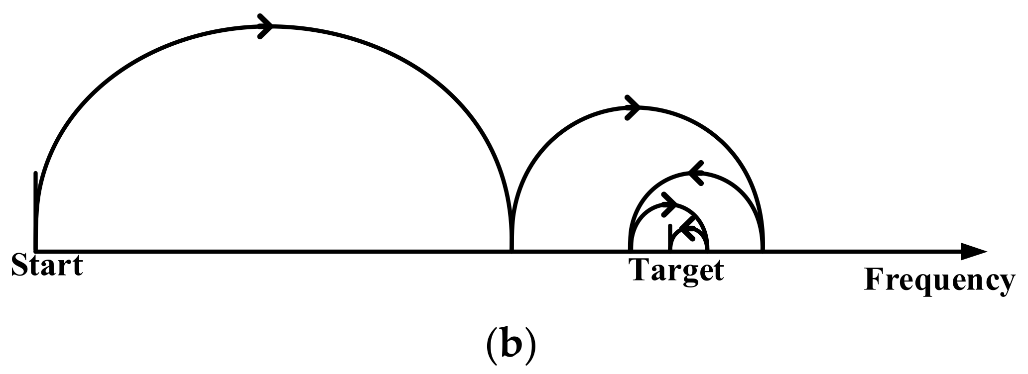
:1. Introduction
2. Circuit Design
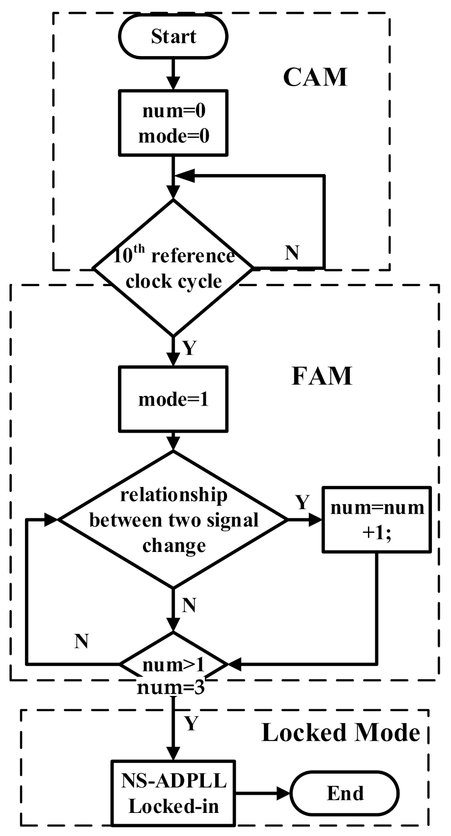
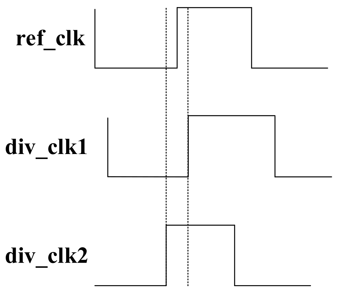
2.1. Control Circuit
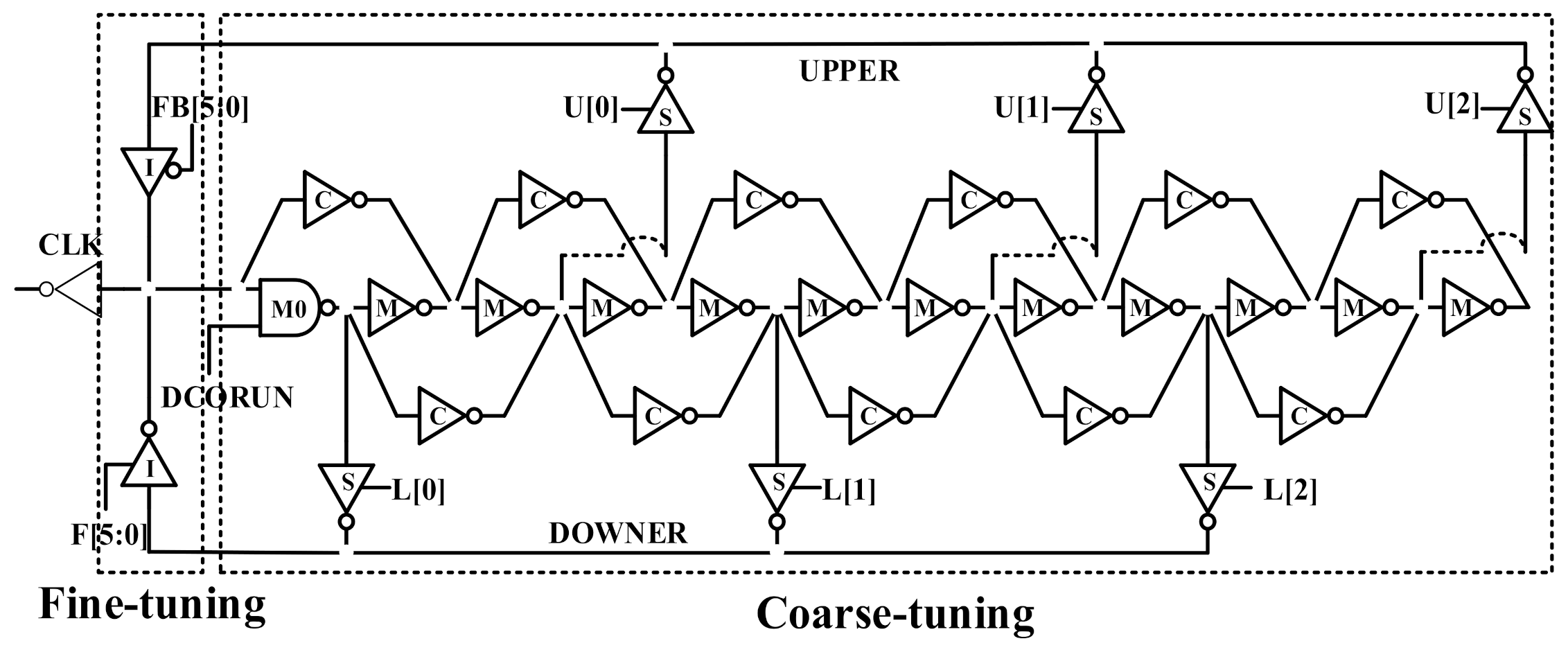
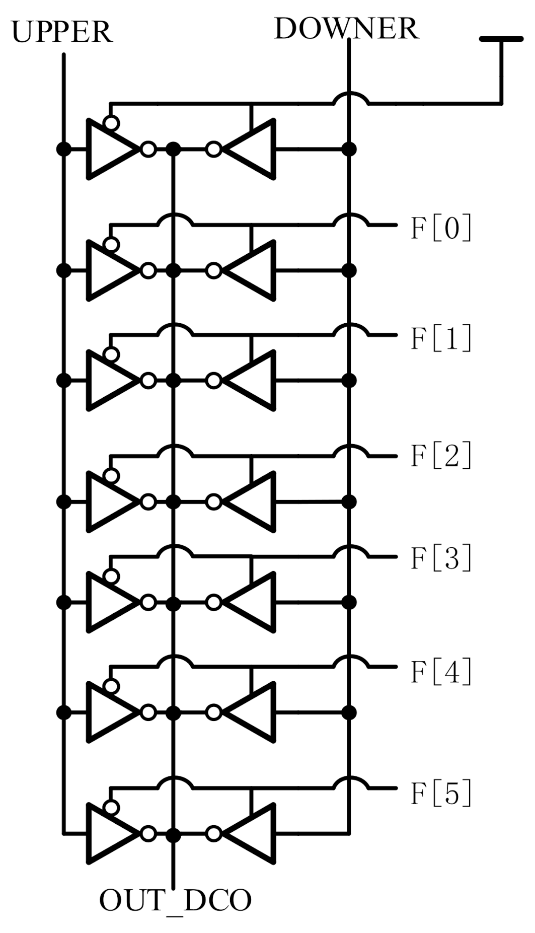
2.2. DCO Circuit
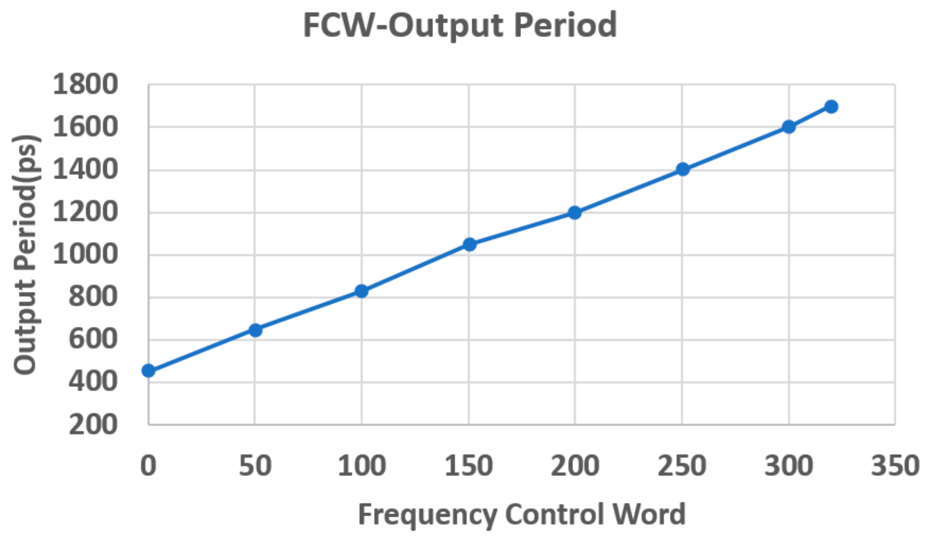
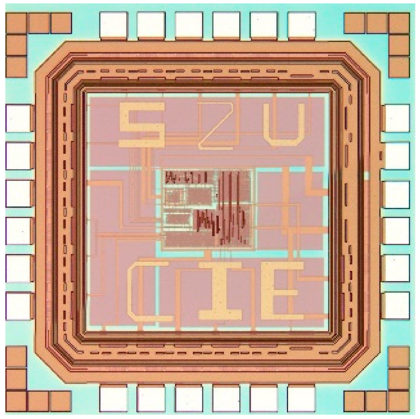
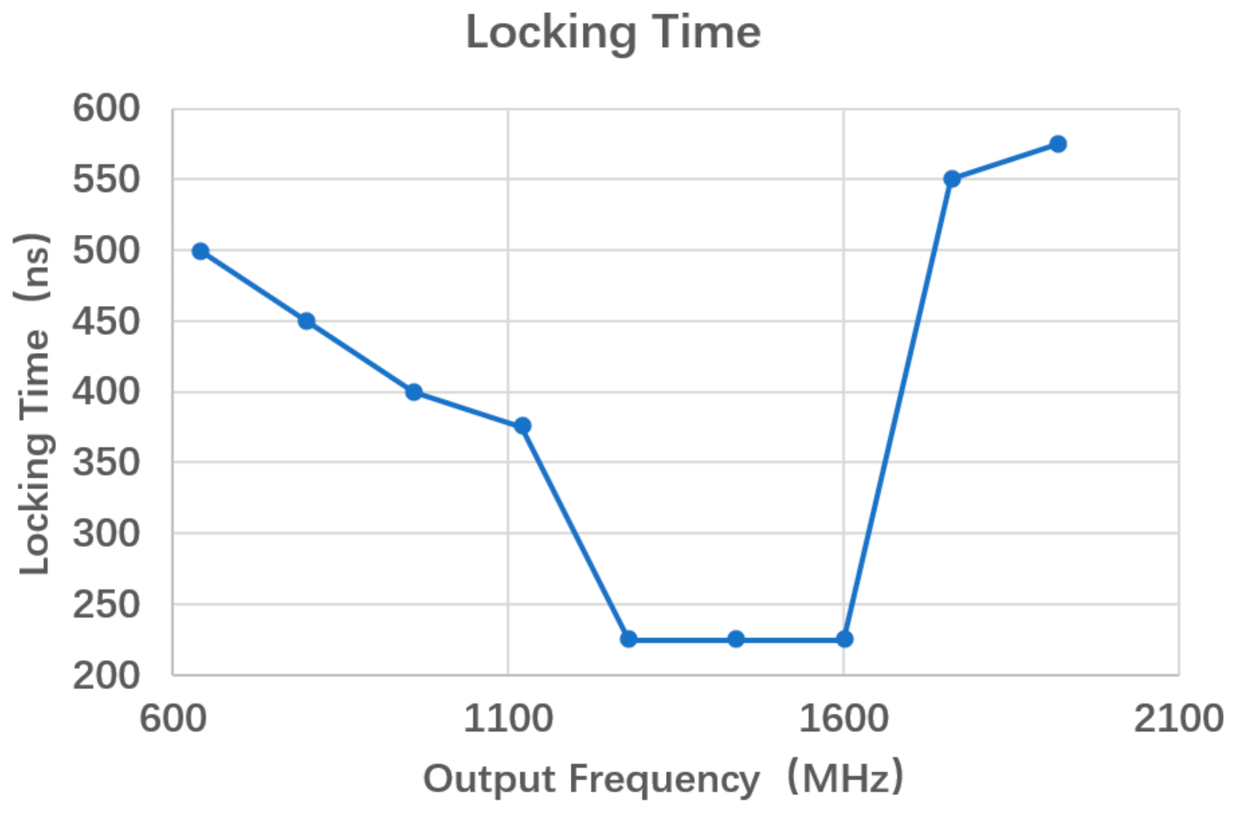
3. Experimental Results
4. Conclusions
Author Contributions
Funding
Data Availability Statement
Conflicts of Interest
References
- Jarrett-Amor, D.; Park, Y.J.; Yuan, F. Time-mode techniques for fast-locking phase-locked loops. In Proceedings of the 2016 IEEE International Symposium on Circuits and Systems(ISCAS), Montreal, QC, Canada, 22–25 May 2016; pp. 1790–1793. [Google Scholar]
- Chen, Y.; Hong, H. A fast-locking all-digital phase locked loop in 90nm CMOS for Gigascale systems. In Proceedings of the 2014 IEEE International Symposium on Circuits and Systems (ISCAS), Melbourne, VIC, Australia, 1–5 June 2014; pp. 1134–1137. [Google Scholar]
- Lotfy, A.; Ghoneima, M.; Abdel-Moneum, M. A fast locking hybrid TDC-BB ADPLL utilizing proportional derivative digital loop filter and power gated DCO. In Proceedings of the 2016 IEEE International Symposium on Circuits and Systems (ISCAS), Montreal, QC, Canada, 22–25 May 2016; pp. 1646–1649. [Google Scholar]
- Chung, C.; Su, W.; Lo, C. A 0.52/1 V Fast Lock-in ADPLL for Supporting Dynamic Voltage and Frequency Scaling. IEEE Trans. VLSI Syst. 2016, 24, 408–412. [Google Scholar] [CrossRef]
- Kim, D.; Song, H.; Kim, T.; Jeong, D. A 0.3–1.4 GHz All-Digital Fractional-N PLL with Adaptive Loop Gain Controller. IEEE J. Solid-State Circuits 2010, 45, 2300–2311. [Google Scholar] [CrossRef]
- Yu, G.; Wang, Y.; Yang, H.; Wang, H. Fast-locking all-digital phase-locked loop with digitally controlled oscillator tuning word estimating and presetting. IET Circuits Devices Syst. 2010, 4, 207–217. [Google Scholar] [CrossRef]
- Hong, S.; Kim, S.; Choi, S.; Cho, H.; Hong, J.; Seo, Y.H.; Kim, B.; Park, H.J.; Sim, J.Y. A 250-μW 2.4-GHz Fast-Lock Fractional-N Frequency Generation for Ultralow-Power Applications. IEEE Trans. Circuits Syst. II 2017, 64, 106–110. [Google Scholar] [CrossRef]
- Ming-Han, C.; Shen-Iuan, L. A 2.4-GHz Area-Efficient and Fast-Locking Subharmonically Injection-Locked Type-I PLL. IEEE Trans. VLSI Syst. 2020, 28, 2474–2478. [Google Scholar]
- Seong, T.; Lee, Y.; Yoo, S.; Choi, J. A −242dB FOM and −75dBc-reference-spur ring-DCO-based all-digital PLL using a fast phase-error correction technique and a low-power optimal-threshold TDC. In Proceedings of the 2018 IEEE International Solid-State Circuits Conference (ISSCC), San Francisco, CA, USA, 11–15 February 2018; pp. 396–398. [Google Scholar]
- Lee, J.; Kim, B. A Low-Noise Fast-Lock Phase-Locked Loop with Adaptive Bandwidth Control. IEEE J. Solid-State Circuits 2000, 35, 1137–1145. [Google Scholar]
- Hwang, I.C.; Song, S.H.; Kim, S.W. A Digitally Controlled Phase-Locked Loop with a Digital Phase-Frequency Detector for Fast Acquisition. IEEE J. Solid-State Circuits 2001, 36, 1574–1581. [Google Scholar] [CrossRef]
- Woo, K.; Liu, Y.; Nam, E.; Ham, D. Fast-Lock Hybrid PLL Combining Fractional-N and Integer-N Modes of Differing Bandwidths. IEEE J. Solid-State Circuits 2008, 43, 379–389. [Google Scholar] [CrossRef]
- Tseng, Y.; Yeh, C.; Liu, S. A 2.25–2.7 GHz Area-Efficient Subharmonically Injection-Locked Fractional-N Frequency Synthesizer with a Fast-Converging Correlation Loop. IEEE Trans. Circuits Syst. I Regul. Pap. 2017, 64, 811–822. [Google Scholar] [CrossRef]
- Zhao, H.; Mandal, S. A Fast-Settling Integer-N Frequency Synthesizer Using Switched-Gain Control. IEEE Trans. Circuits Syst. I Regul. Pap. 2020, 67, 1344–1357. [Google Scholar] [CrossRef]
- Zhang, Y.; Tang, X.; Wei, Z.; Bao, K.; Jiang, N. A Ku-Band Fractional-N Frequency Synthesizer with Adaptive Loop Bandwidth Control. Electronics 2020, 10, 1–14. [Google Scholar]
- Seo, S.; Chun, J.; Jun, Y.; Kim, S.; Kwon, K. A Digitally Controlled Oscillator with Wide Frequency Range and Low Supply Sensitivity. IEEE Trans. Circuits Syst. II 2011, 58, 632–636. [Google Scholar] [CrossRef]


| Symbol | Quantity | Data |
|---|---|---|
| ps | Coarse-tuning | 224 |
| ps | Fine-tuning | Best 1 ps, Worst 8 ps |
| GHz | Output frequency range | 0.5–2 |
| Area | 0.006 |
| [1] | [3] | [4] | [8] | This Work | |
|---|---|---|---|---|---|
| Process (nm) | 130 | 65 | 90 | 45 | 180 |
| Supply (v) | 1.8 | - | 1.2 | 1.8 | |
| Area () | - | 0.013 | 0.065 | 0.013 | 0.04 |
| Power (mW) | 1.37 | 5.1 | 0.92 | 5.6 | 29.48 |
| Input (MHz) | 500 | 200 | 20 | 150 | 40 |
| Output (GHz) | 1.8 | 2.76–6 | 0.06–0.6 | 2.4 | 0.64–1.92 |
| RMS jitter (ps) | - | 1.37 | 13.7 | 0.91 | 15.6@1.6 GHz |
| Ref cycles (Locked) | 150 | 200 | 16 | 270 | 9@1.6 GHz |
| Time (ns) | 300 | 1000 | 800 | 1800 | 225@1.6 GHz |
Publisher’s Note: MDPI stays neutral with regard to jurisdictional claims in published maps and institutional affiliations. |
© 2021 by the authors. Licensee MDPI, Basel, Switzerland. This article is an open access article distributed under the terms and conditions of the Creative Commons Attribution (CC BY) license (https://creativecommons.org/licenses/by/4.0/).
Share and Cite
Deng, X.; Li, H.; Zhu, M. A Novel Fast-Locking ADPLL Based on Bisection Method. Electronics 2021, 10, 1382. https://doi.org/10.3390/electronics10121382
Deng X, Li H, Zhu M. A Novel Fast-Locking ADPLL Based on Bisection Method. Electronics. 2021; 10(12):1382. https://doi.org/10.3390/electronics10121382
Chicago/Turabian StyleDeng, Xiaoying, Huazhang Li, and Mingcheng Zhu. 2021. "A Novel Fast-Locking ADPLL Based on Bisection Method" Electronics 10, no. 12: 1382. https://doi.org/10.3390/electronics10121382
APA StyleDeng, X., Li, H., & Zhu, M. (2021). A Novel Fast-Locking ADPLL Based on Bisection Method. Electronics, 10(12), 1382. https://doi.org/10.3390/electronics10121382