Article

Low-Power Two-Phase Clocking Adiabatic PUF Circuit

by
Câncio Monteiro
1,* and
Yasuhiro Takahashi
2
1
Department of Electrical and Electronics Engineering (EEE), Faculty of Engineering, Science and Technology, Universidade Nacional Timor Lorosa’e (UNTL), Avenida Hera, Cristo-Rei, Dili, Timor-Leste
2
Department of Electrical, Electronics and Computer Engineering (EECE), Faculty of Engineering, Gifu University, 1-1 Yanagido, Gifu-shi 501-1193, Japan
*
Author to whom correspondence should be addressed.
Electronics 2021, 10(11), 1258; https://doi.org/10.3390/electronics10111258
Submission received: 19 April 2021 / Revised: 21 May 2021 / Accepted: 23 May 2021 / Published: 25 May 2021
(This article belongs to the Section Circuit and Signal Processing)

Abstract

:
Internet of Things (IoT) has enabled battery-powered devices to transmit sensitive data, while presenting high power consumption and security issues. To address these challenges, adiabatic-based physical unclonable functions (PUFs) offer a promising solution for low-power and secure IoT device applications. In this study, we propose a novel low-power two-phase clocking adiabatic PUF. The proposed adiabatic PUF utilizes a trapezoidal power clock signal with a time-ramped voltage to achieve an improved energy efficiency and reliable start-up PUF behavior. Static CMOS logic is employed to produce stable challenge-response pairs (CRPs) in the adiabatic mode. The pull-down network is designed to control the PUF cell to charge and discharge its output nodes with a constant supply current during secure key generation. The body effect of PMOS transistors, ambient temperatures, and CMOS process variations are investigated to examine the uniqueness and reliability of the proposed work. The proposed adiabatic PUF is simulated using 0.18 µm CMOS process technology with a supply voltage of 1.8 V. The uniqueness and reliability of the proposed adiabatic PUF are 49.82% and 99.47%, respectively. In addition, it requires a start-up power of 0.47 µW and consumes an energy of 15.98 fJ/bit/cycle at the reference temperature of 27 °C.

1. Introduction

The emerging Internet of Things (IoT) technology has simultaneously introduced challenges and opportunities for engineering-related fields. IoT is used to create smart interconnected and resilient communication systems (e.g., smart home security systems, smart health, smart cities, smart transportation, smart factories, smart grids, etc.) through the internet to improve the quality of people’s lives. IoT devices include smartphones, smart cards, biomedical devices, radio frequency identification (RFID) tags, and many other cryptographic devices that require security characteristics, such as authenticity, integrity, and confidentiality in performing their tasks [1,2]. IoT interconnected devices transmit sensitive data that can be targets of cyber-attacks [3]. In addition, typical countermeasures include cryptographic methods, often based on random numbers, which are necessary to generate public and private keys. Therefore, a physical unclonable function (PUF) plays a key role in authentication and secure key generation [4,5]. The taxonomy of PUF in a study stated that a PUF is a hardware security fundamental that translates an input challenge into an output response through a physical system in a manner that is specific to the exact hardware instance (unique) and cannot be replicated (unclonable) [6]. An advantage of employing a PUF in a cryptosystem is its nonvolatile memory-based key storage feature, as the PUF generates keys on demand during stimulation. The characteristic of a PUF include unpredictable response (R) of the system owing to intrinsic variations, which are stimulated by the input challenge (C). The challenge–response system is modeled as a black box; hence, the PUF input-output relation is described as R = f(C), where f(.) is an unknown internal parameter influenced by the intrinsic variations of the device [4,7].
Many studies on PUF cell level have been conducted, such as investigations on the arbiter PUF [8,9,10], ring-oscillator (RO) PUF [11,12,13,14,15], Gunlu et al. employed RO in field-programmable gate array for transform-coding [16], be-stable ring PUF [17], glitch PUF [18], dynamic random access memory (DRAM) PUF [19,20], and static random access memory (SRAM) PUF [21,22]. In addition, many studies on low-power PUF circuits have been conducted, such as robust digital response and low-power current-based PUF [23], as well as the SRAM-based PUFs over a wide range of supply voltages from the super-threshold voltage regime down to the near-threshold voltage (NTV) regime [24]. The IoT devices are mostly battery-powered embedded devices and operate in low frequency ranges, which cause security issues and low power consumption. All PUF cells presented in [8,9,10,11,12,13,14,15,16,17,18,19,20,21,22] undergo high-power consumption and voltage ramp-up time adaptation for a reliable PUF circuit. In this study, we have attempted to address these two issues.
For low-power and low-frequency applications, the adiabatic switching technique [25] is considered to be an appropriate logic design approach for cryptographic circuit implementation [26,27,28]. In 2016, the first low-power adiabatic SRAM PUF cell was introduced, which was a quasi-adiabatic logic-based PUF (QUALPUF) [29]. The security measures of 128-bit QUALPUF were further investigated thoroughly in [30], and the 4-bit QUALPUF LSI was implemented in a 0.18 µm standard CMOS process with 1.8 V nominal supply voltage along with post-layout and chip measurements in [31,32]. The merit of the QUALPUF is an energy-efficient computation platform, which used adiabatically time-ramp voltage to improve the reliability of a PUF cell.
In this study, we designed an ultra-low-power PUF cell based on the adiabatic switching principle to generate a reliable cryptographic key for IoT embedded devices. The proposed adiabatic PUF circuit is based on an SRAM cell in which the PUF response is stimulated by a challenge bit via a static CMOS circuit. The QUALPUF circuit is benchmarked for comparison in terms of energy efficiency and security evaluation metrics (uniqueness and reliability). The comparison was performed under the temperature range of −40–100 °C (27 °C was considered as the reference), load capacitance range of 10–200 fF, and CMOS process variations of 10% (threshold voltage (VTH) and gate oxide thickness (TOX) variations).
The remainder of this paper is structured as follows: Section 2 describes the fundamental adiabatic PUF by first explaining the fundamental adiabatic switching and conventional adiabatic PUF, and then introducing the operation principle of the proposed adiabatic PUF. The circuit topology of a 4-bit proposed adiabatic PUF cell is presented in Section 3. The simulation conditions, security evaluation metrics, and simulation results are described in Section 4. The evaluation of the proposed work in comparison with conventional PUFs is discussed in Section 5. Finally, Section 6 concludes the research findings of this work.

2. Fundamental Adiabatic PUF

2.1. Principle of Adiabatic Switching

Adiabatic switching is commonly used to minimize the energy loss during charging/discharging process [25]. During adiabatic switching, all nodes are charged or discharged at a constant current to minimize the power dissipation. This is accomplished using AC power supplies that initially charge the circuit during specific adiabatic phases and then discharge the circuit to recover the supplied charge. The principle of adiabatic switching can best be explained by comparing the internal equivalent RC model for charging and discharging the output load capacitance, as shown in Figure 1a,b, for conventional CMOS and adiabatic switching, respectively. The difference between the adiabatic switching and conventional CMOS RC model is that the latter uses the step voltage of Vdd, whereas the former uses a power clock signal as the source voltage in which the ramped step voltage gradually increases (indicated by τ), as shown in Figure 1b.
Applying the Kirchhoff voltage law (KVL) to the circuit in Figure 1a,b, the charging network of the conventional CMOS is expressed as follows:
R i ( t ) + 1 C 0 τ i ( t ) d t + v ( 0 ) = V dd
and the charging network for adiabatic switching is expressed as
R i ( t ) + 1 C 0 τ i ( t ) d t + v ( 0 ) = V dd τ t
where τ is the rising time of the ramp voltage Vdd. The Laplace transform and inverse Laplace transform are employed to obtain the charging current for CMOS logic and adiabatic logic, as expressed in Equations (3) and (4), respectively.
i ( t ) = V dd R e 1 R C t
i ( t ) = V dd C τ ( 1 e 1 R C t )
The peak current difference shown in Equations (3) and (4) indicate a large area and sudden flow of current in the conventional CMOS. In addition, a gradual increase in the supply current peak of the adiabatic switching can be observed in Figure 1c.
From the energy consumption perspective, the dissipated energy over the period t = 0 to t = τ is expressed as follows:
E d i s s = 0 τ R i 2 ( t ) d t + E ( 0 )
Substituting the current i(t) from Equations (3) and (4) into Equation (5), we obtain the energy stored in the capacitor for the conventional CMOS and adiabatic switching, as expressed in Equations (6) and (7), respectively.
E C M O S = 1 2 C V dd 2
E A d i a b a t i c = R C τ C V dd 2
Equations (6) and (7) clearly show that the dissipated energy of the conventional CMOS (Equation (6)) depends on the values of C and Vdd, while that of the adiabatic logic depends on the switching time τ. Hence, by increasing the switching time (where τ > RC), the energy dissipation of adiabatic logic is significantly lower than that of the conventional CMOS logic.

2.2. Conventional Adiabatic PUF

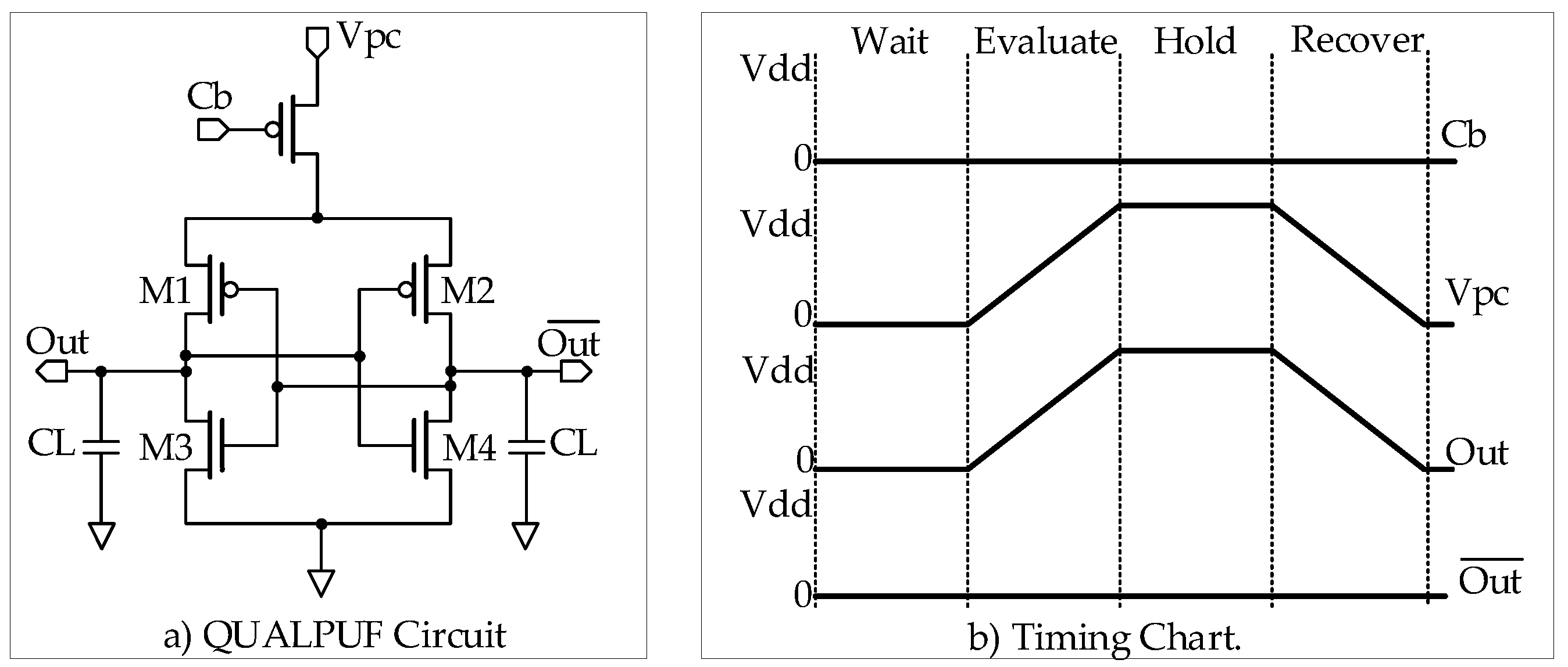
In 2016, the first PUF circuit (quasi-adiabatic logic PUF (QUALPUF)) that employed the adiabatic switching technique was reported in [29], in which the PUF cell was composed of a cross-coupled inverter (M1, M2, M3, and M4), and a pull-up network transistor to enable or disable the PUF cell. The fundamental QUALPUF circuit topology and its timing chart are shown in Figure 2a,b, respectively. Figure 2b describes the four phases (wait, evaluate, hold, and recovery) of the adiabatic switching operation during challenge-bit (Cb) in the logic low state. Moreover, the adiabatic PUF is supplied with trapezoidal power clock signals that enable PUF response bits to be all zero-level once challenge-bit gets logic “1”. However, the response-bit of the QUALPUF stays at VTH of M3 (approximately 0.45 V), which yields few floating charges during the recovery phase. The stored charge is not fully discharged/recovered back to the power supply. The novel QUALPUF was again thoroughly investigated using 180 nm and 45 nm CMOS technology in a cadence spectrum simulator to analyze the effect of channel length variations [31]. The post-layout simulation result of 4-bits cascaded QUALPUF was reported in [30], and the fabricated chip of 4-bits cascaded QUALPUF LSI using 0.18 μm ROHM standard CMOS process was tested in [32].

2.3. Proposed Adiabatic PUF

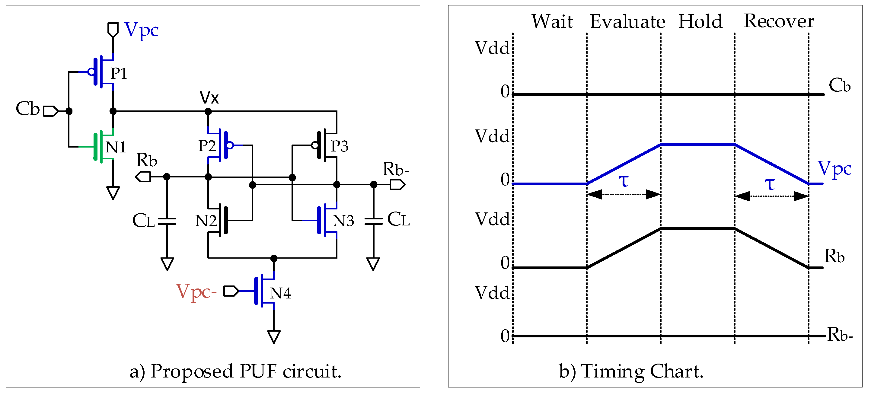
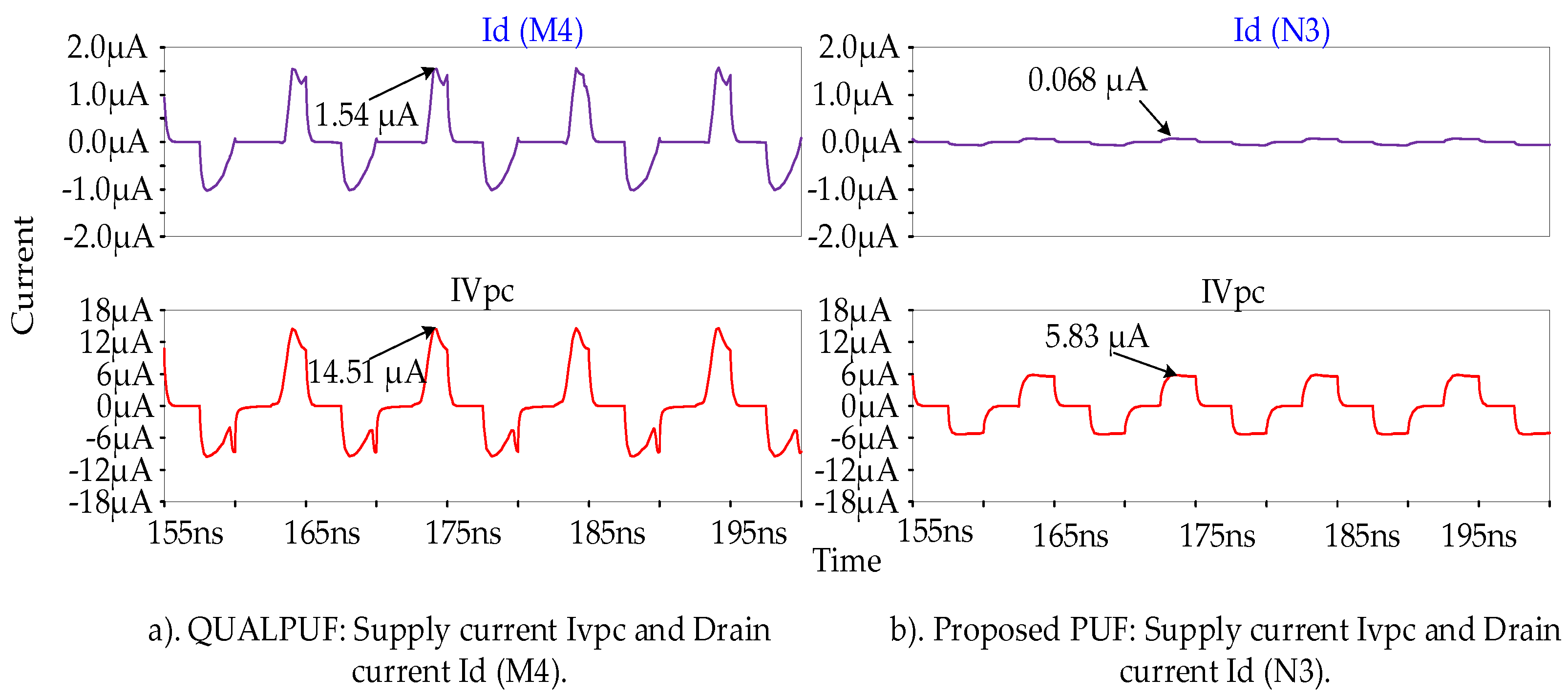
The proposed adiabatic PUF circuit topology is shown in Figure 3a. It consists of a static CMOS inverter (P1 and N1), which plays a key role in charging and discharging the PUF cell semi-adiabatically using a trapezoidal power clock signal of Vpc and controlled by the Cb. Similar to the QUALPUF circuit, the proposed PUF cell consists of a cross-coupled inverter (P2, P3, N2, and N3) to evaluate the response-bits (output nodes of Rb and Rb- in Figure 3a). As an improvement, we control the current flow from one of the output nodes to slowly flow to the ground through transistor N4 by controlling its operation speed with a ramped Vpc- signal. Furthermore, the peak value of current Id (N3) in Figure 3a is significantly lower than that of current Id (M4) of QUALPUF depicted in Figure 2a. Notably, in our proposed adiabatic PUF circuit, we apply two phases of power clock signals Vpc and Vpc-, as depicted in Figure 7b.
The supply voltage Vpc swings between 0.9 and 1.8 V (peak to peak voltage is 0.9 V), while the Vpc- fluctuates between 0 and 0.9 V. The Vpc and Vpc- signals are set such that all output nodes are discharged back to Vpc and ground simultaneously to avoid floating charges for the next charging operation. Accordingly, the proposed adiabatic PUF circuit will consume constant and extremely low power along the period of challenge-bit logic “0”.

2.3.1. Operation of the Proposed Adiabatic PUF

To better understand the proposed adiabatic logic-based PUF, we describe the proposed circuit operation in four different adiabatic phases (Wait, Evaluate, Hold, and Recover, as shown in Figure 3b) when the challenge-bit is at logic “0”, which enables the P1 transistor (Figure 3a) to create a path for the adiabatic operation.
  • Wait Phase: During the wait phase, the power clock (Vpc) is at a constant level of 0.9 V. Therefore, the PUF cell will be in a waiting state during this phase.
  • Evaluate Phase: During the evaluate phase, Vpc slowly rises from 0.9 to 1.8 V (Vdd). Because Vpc is always greater than VTHP in our proposed Vpc signal, both P2 and P3 are turned ON. However, owing to the effect of different threshold voltages due to imperfections in the CMOS manufacturing process, one of the transistors (P2 and P3) with a lower threshold voltage will conduct first, thereby facilitating the corresponding load capacitor to quickly become charged. This will lead to a flip in the outputs where one of the outputs leads to logic “1” and the other to logic “0”. In this phase, the supply current IVpc flows through P1 and P2 to charge the Rb node capacitor, as shown in Figure 3a.
  • Hold Phase: During the hold phase of the Vpc, the proposed adiabatic PUF generates a stable PUF response.
  • Recover Phase: During the recovery phase of the Vpc, the time ramp voltage slowly decreases from Vdd to 0.9 V. During this phase, the charge stored in the load capacitor is slowly recovered back to the power clock supply through P1 and P2 transistors. Moreover, the response bits will remain stable because the low level of Vpc is 0.9 V, which is always higher than the VTH of both NMOS and PMOS transistors. Hence, the Rb node maintains logic “1”, which triggers transistor N3 to stay always ON and pull-down Rb- node to ground level through transistor N4 once Vpc- is higher than VTHN.
When the challenge bit increases, transistor P1 turns OFF, and N1 turns ON. In this condition, the output node of the response bit Rb will be discharged from 0.9 V to ground via P2 and N1 transistors. All output nodes (Rb and Rb-) will be at logic “0” and flipped once the challenge bit Cb declines again to logic “0” for the next adiabatic operation.

2.3.2. Theoretical Analysis of the Proposed Adiabatic PUF

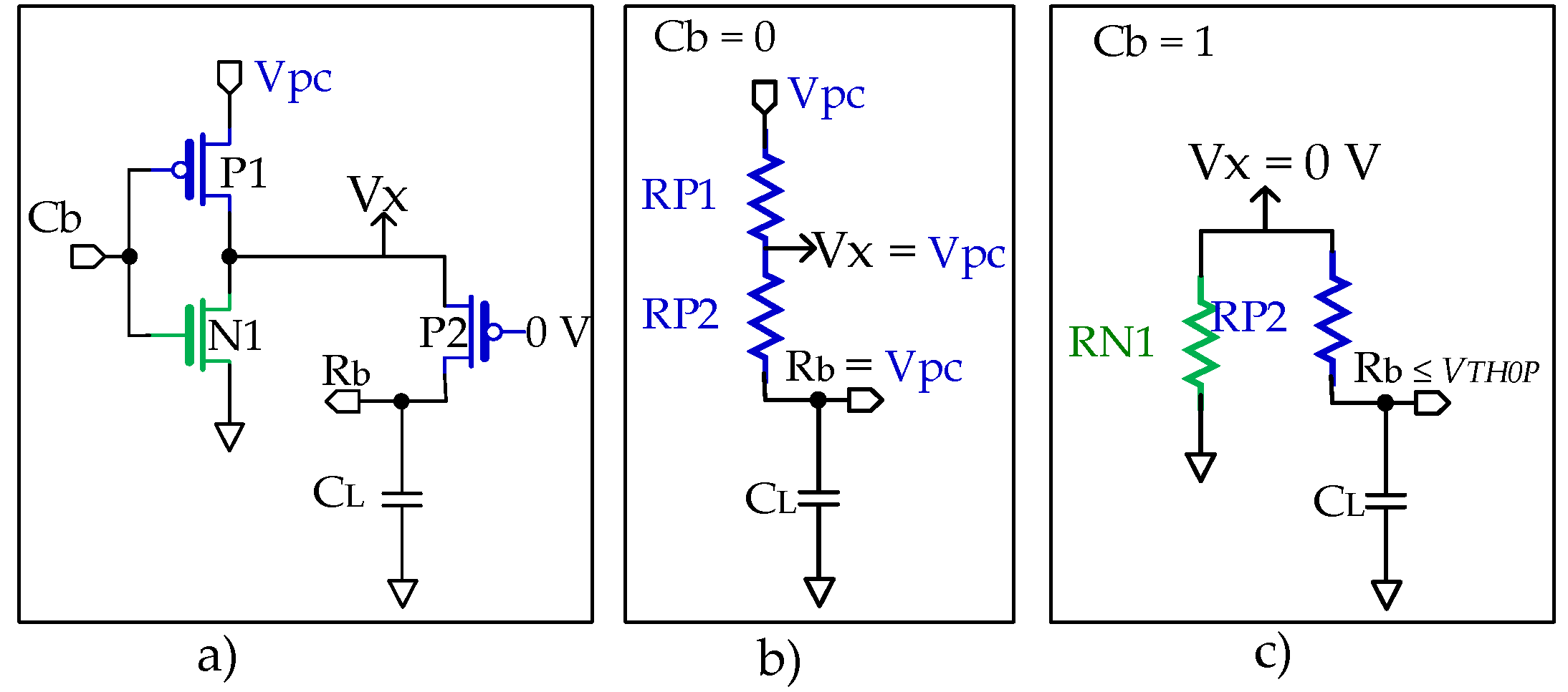
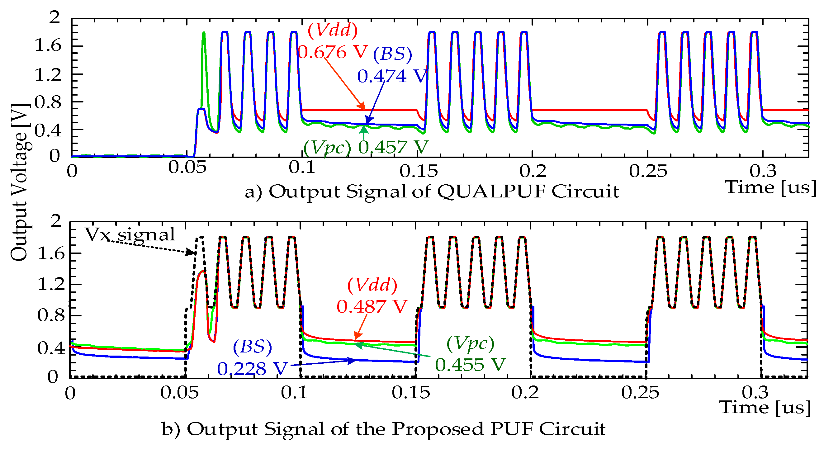
In most of today’s CMOS processes, the PMOS devices are physically separated from each other by fabricating in an n-well [33]. This facilitates individual connection between the bulk and source of each PMOS device. Accordingly, we have investigated the body effect of a PMOS by connecting the body of a PMOS to Vdd (constant voltage) of the Vpc power clock, and to the source of each PMOS (P1, P2, and P3 in Figure 3a). Figure 5 shows the output signals (response bit Rb signals) of the proposed adiabatic PUF versus the QUALPUF circuit. As labeled in Figure 5a,b, (BS): PMOS bulk is tied to each respective Source, (Vpc): all PMOS bulks are tied to Vpc signal, and (Vdd): all PMOS bulks are tied to constant Vdd. The circuit operation is shown in Figure 4. Let Cb = 0. Then, P1 and P2 are ON, and CL is charged from Vpc (the RC model in Figure 4b, and such signal is shown at t = 0.15–0.2 µs, as shown in Figure 5). In contrast, Figure 4c illustrates that when Cb = Vdd, P2 and N1 are ON, forcing CL to discharge to ground level (such signal is shown at t = 0.1–0.15 µs, as shown in Figure 5). We attempted here to reduce the output voltage level of Rb (Figure 4c) as close to zero as possible (when challenge bit Cb = 1, i.e., Cb logic “1” or Vdd). However, the response bit Rb cannot be declined to ground because of a voltage drop at RP2, which is associated with the VTH of PMOS P2. The MOS VTH variation is expressed as follows:
V TH = V TH 0 + γ ( | 2 Φ F + V SB | | 2 Φ F | )
where γ and ΦF are MOSFET device parameters, and VSB is the source-bulk potential difference [34]. In our proposed PUF design, the PMOS body is connected to its source pin, as shown in Figure 4a,c, indicating that VSB = 0 V; hence, the VTH of P2 is ≤VTH0, which is the lowest output voltage level, as depicted in Figure 5. Therefore, the bulk of PMOS that is tied to each source is chosen for further simulations.

3. Design of 4-Bits Adiabatic PUF

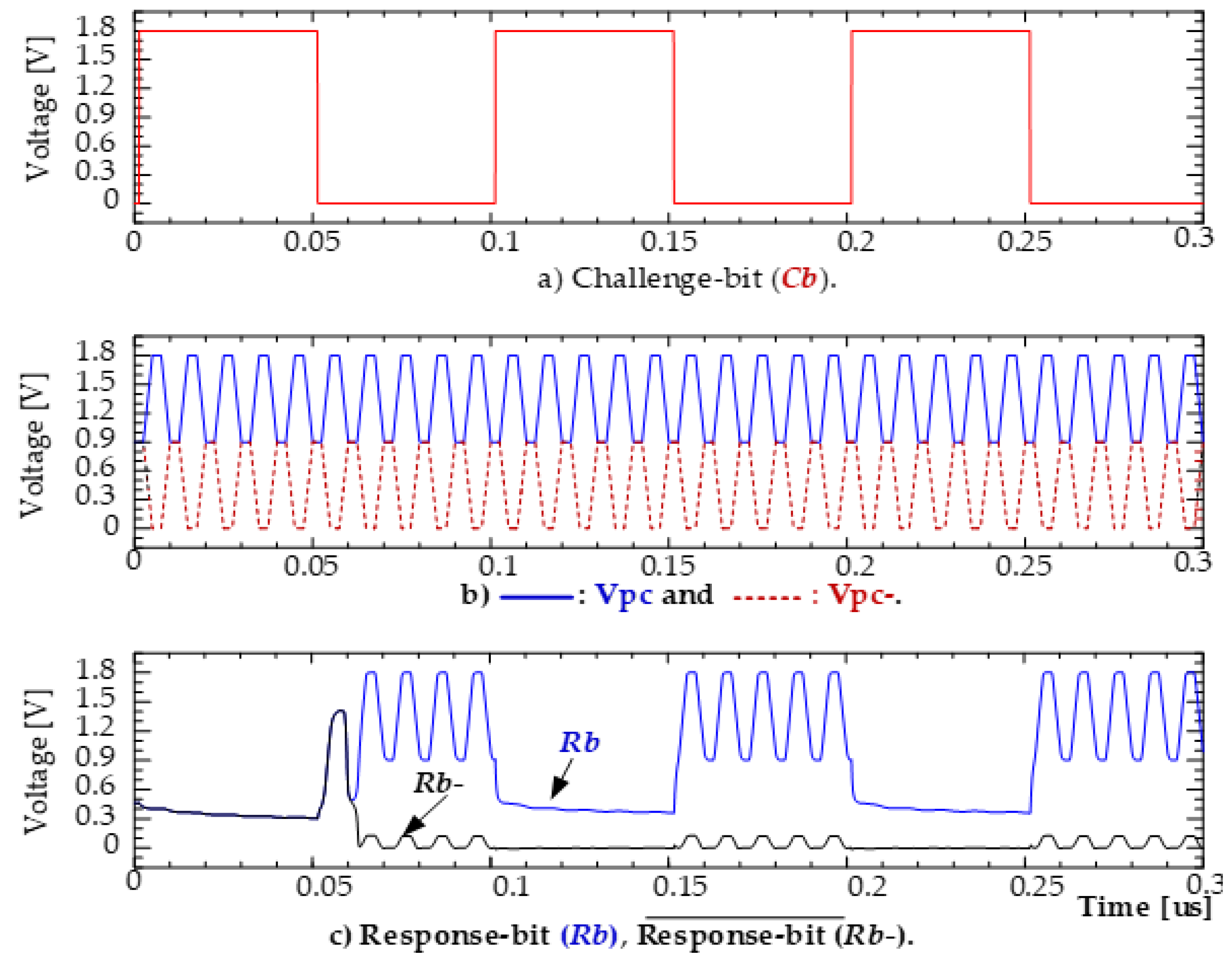
To validate the proposed adiabatic PUF cell, we designed a 4-bit cascaded adiabatic PUF, as depicted in Figure 6. Each local PUF is supplied by four power clocks, where each adjacent clock differs by a phase difference of 90°. For instance, if the first cell, as shown in Figure 6, operates in the hold phase, the next cell in the same local PUF operates in the recovery phase. Similarly, the other two PUFs operate in the wait and evaluation phases, respectively. When all four outputs are sampled at a time, it leads to a length of 4 bits. Moreover, each local PUF cell is controlled by challenge bits; each adjacent bit has ¼ delay time of one power clock cycle. Therefore, if one cycle of Vpc signal has 10 ns, then the second Cb signal will have a delay time of 2.5 ns, compared to the first Cb signal. This delay time allows the challenge bits to flip the response signals at the middle point of the wait phase of the Vpc signals, as shown in Figure 7a,b. Thus, the challenge bits are flipped adiabatically, as depicted in Figure 7c, thereby significantly reducing the energy.

4. Simulation and Results

4.1. Simulation Condition

To analyze the effectiveness of the proposed adiabatic PUF, a 4-bit cascaded PUF was simulated using a 0.18 μm standard CMOS process provided by ROHM Corporation. Table 1 summarizes the MOS device parameters and simulation conditions.
The ability of PUF to uniquely distinguish a chip among the group of other chips was demonstrated by conducting 100-runs of the Monte Carlo simulation to emulate the behavior of 100 IC PUF chips. This simulation aimed to analyze the effect of process variation, such as VTH, TOX, and ambient temperature variations. For VTH and TOX, a tolerance variation of 10% was set in the Monte Carlo simulation to evaluate the uniqueness and reliability of the proposed adiabatic PUF cell. The temperature variation was set at −40, 0, 27, 50, and 100 °C.

4.2. Simulation Result

The relationship between the input challenge bits and output response bits of the proposed adiabatic PUF cell is in the correct logic function, as depicted in Figure 7. For performance analysis, the energy dissipation per cycle per challenge bits (logics “1” and “0”) and the PUF evaluation metrics of uniqueness and reliability are presented.

4.2.1. Energy Dissipation

A major reason for employing adiabatic switching techniques in PUF circuits is to reduce power consumption. In this study, energy is collected from the total instantaneous power along the duration of the challenge bit cycle as follows:
E = 0 T ( ( V p c s I p c s ) ) d t
where T is the period of challenge bit (fCb = 10 MHz or inversely equal to 100 ns).
Start-up energy and energy per cycle are considered in this study. For instance, Figure 7 shows that the start-up energy is the total power consumed in the time range of 0–0.1 µs, and the energy-per-cycle is the total power consumed in the time range of 0.1–0.2 µs, or average of cyclical energy of challenge-bit after start-up period. Instead of the start-up energy, we consider the start-up power in this study, which is derived from the energy-per-cycle/time period.
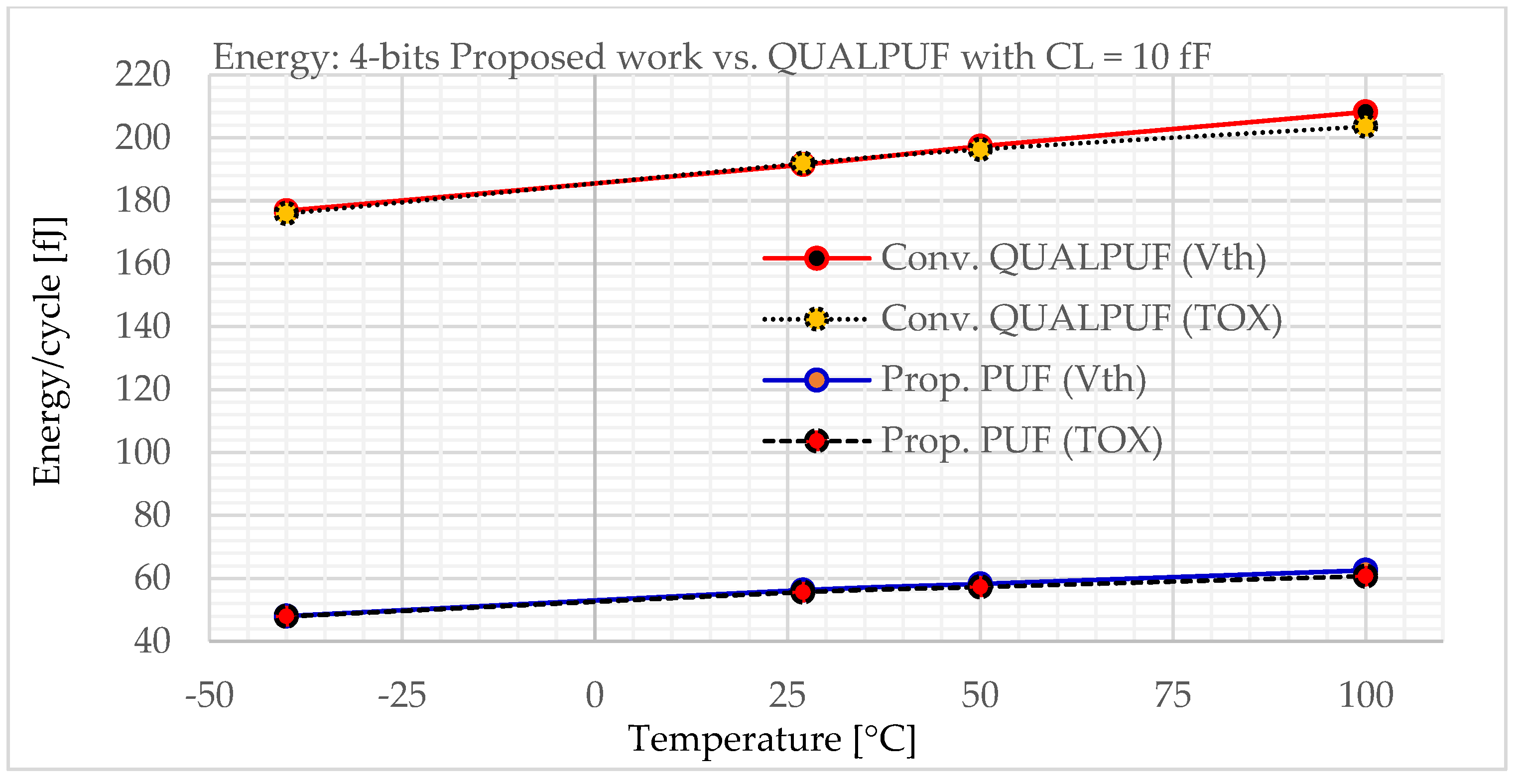
We evaluated the energy consumption of the proposed adiabatic PUF circuit in comparison with the QUALPUF circuit at the PUF cell level (1-bit) and 4-bit cascaded PUF circuit, as graphically illustrated in Figure 8 and Figure 9, respectively. Figure 8 shows the 1-bit PUF cell energy comparison of the proposed PUF and QUALPUF with respect to the body effect of the PMOS transistors along with the temperature variation. Figure 9 illustrates the energy comparison of both the 4-bit circuit topologies. The energy loss shown in Figure 9 is the average of the energy consumed by 100 chips emulated using Monte Carlo simulation with VTH and TOX variations of 10%. The energy data of the proposed PUF in Figure 8 and Figure 9 were obtained from the proposed circuit with all PMOS bulks tied to each respective source pin. In addition, both VTH and TOX variations consume comparable amounts of energy with respect to the temperature change.

4.2.2. PUF Evaluation Metric

We utilize two evaluation metrics to verify the proposed adiabatic PUF behavior.
  • Uniqueness is used to determine the ability of a PUF to distinguish a chip from other chips [29]. The ideal value of the uniqueness metric is 50%, indicating that a uniqueness result closer to 50% has a better performance (where the normalized value of uniqueness is 0 ≤ U ≤ 1). The uniqueness is expressed as
    U n i q u n e s s = 2 k ( k 1 ) i = 1 k 1 j = i + 1 k H D ( R i ,   R j ) n × 100
    where HD(Ri, Rj) represents the Hamming Distance of the two different PUF instances’ responses, with k number of chips and n-bit length.
  • Reliability measures how reproducibly the challenge-response pairs of a PUF instance with varying environmental conditions, such as temperature and CMOS process variations. The reliability is mathematically expressed as follows:
    R e l i a b i l i t y = 100 1 k i = 1 k H D ( R i ,   R i , j ) n
    where k represents the total number chips (k = 100 in this study), n is the number of PUF bits, and HD(Ri, Ri,j) is the Hamming Distance of j-th sampling of Ri. The ideal reliability value is 100%.
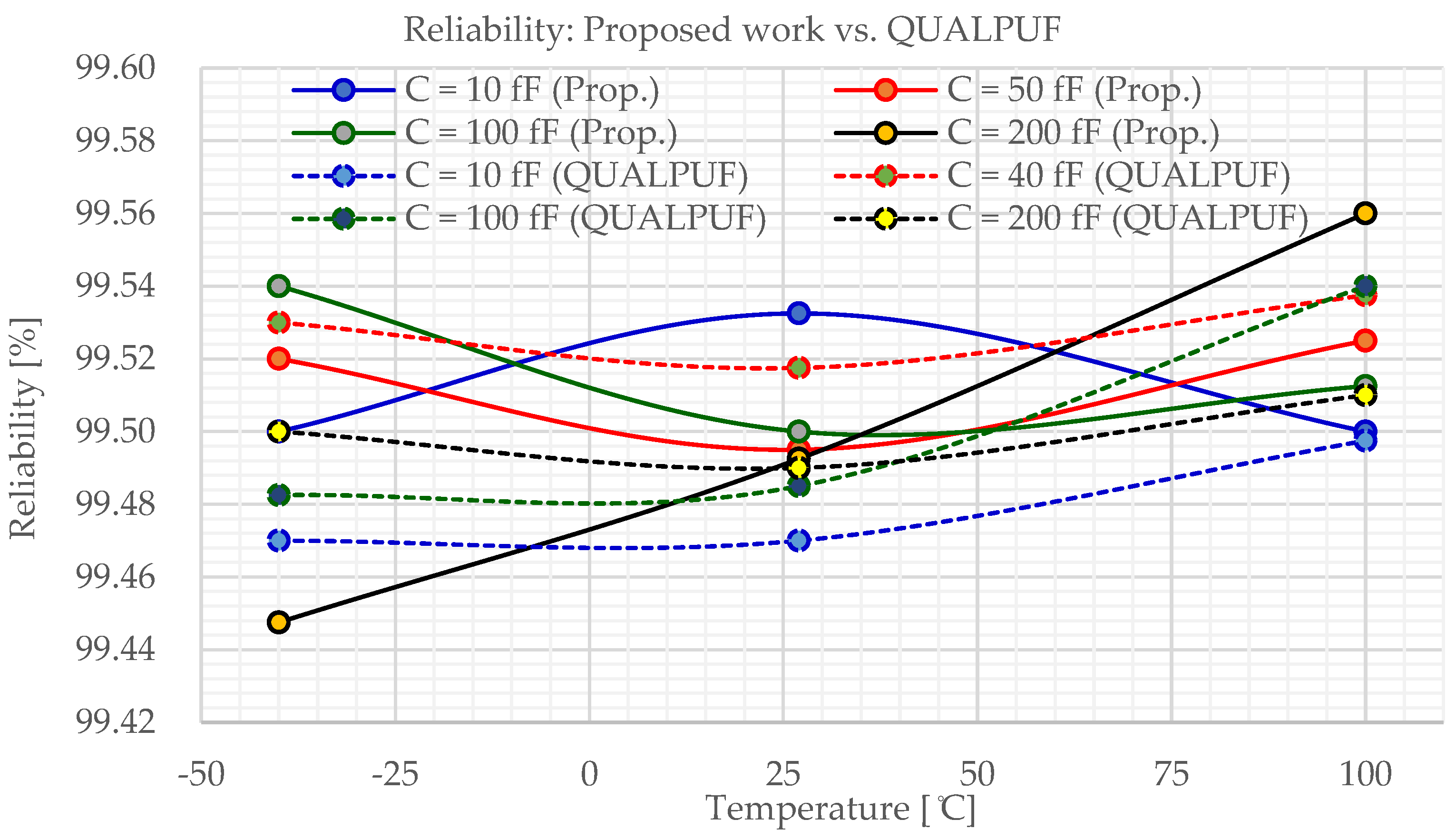
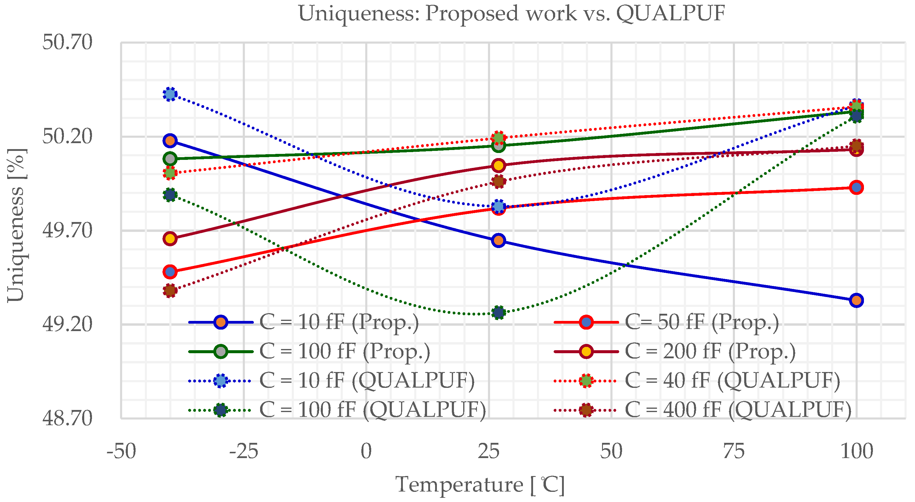
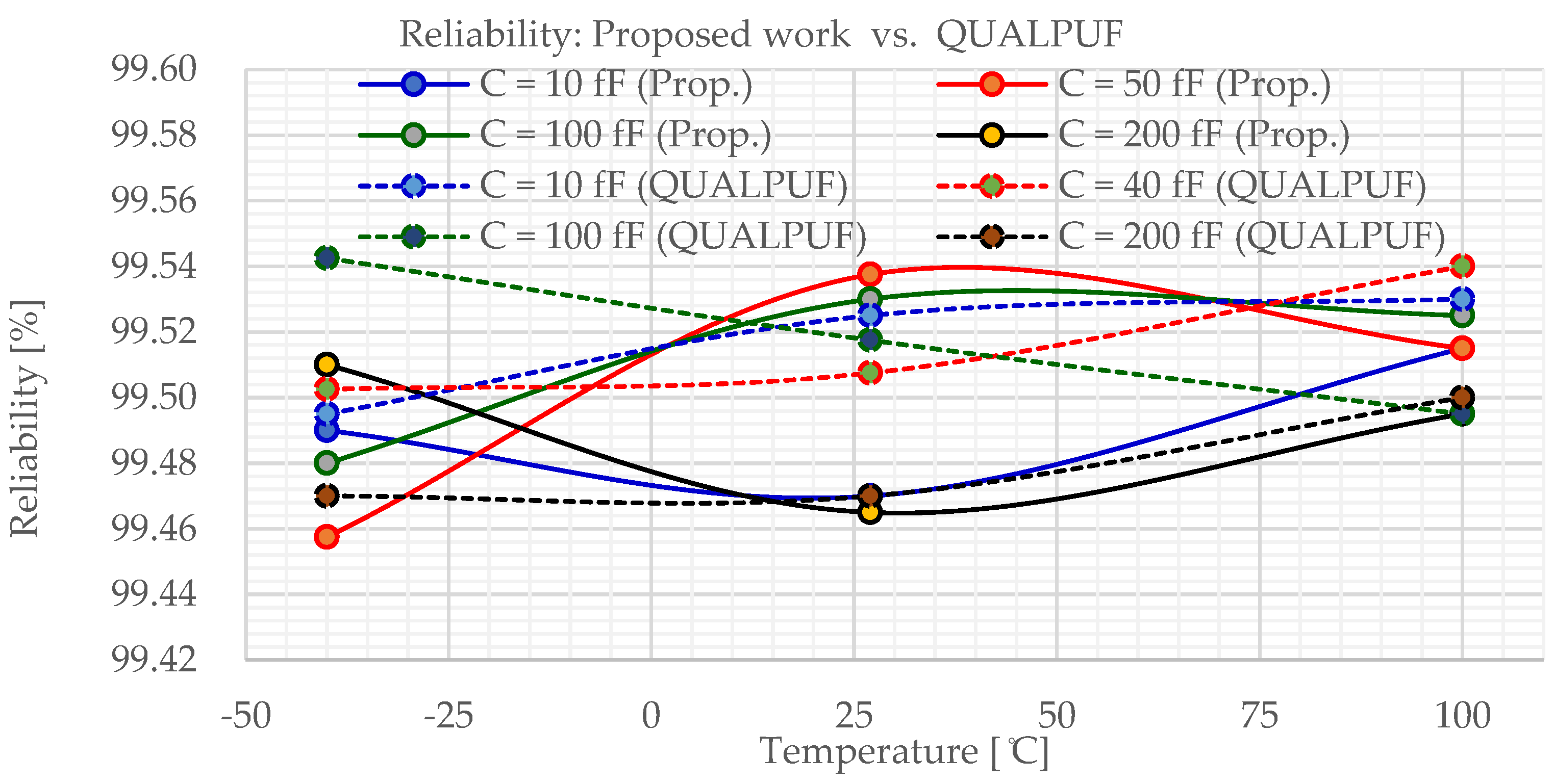
The calculated uniqueness results using Equation (9) are graphically depicted in Figure 10 and Figure 12, and calculated reliabilities (using Equation (10)) are shown in Figure 11 and Figure 13, under VTH and TOX variations, respectively. In this study, we used a bit size of n = 4 and chip number of k = 100. In Figure 10, Figure 11, Figure 12 and Figure 13, the solid lines indicate the proposed adiabatic PUF, and the dotted lines represent QUALPUF. To facilitate the uniqueness and reliability calculations, Monte Carlo simulations were repeatedly conducted with a varying output load capacitance (CL = 10, 50, 100, and 200 pF) under temperature variations.

5. Discussion

We investigate the power efficiency of the proposed adiabatic PUF cell and reliability of the PUF circuit using PUF evaluation metrics (uniqueness and reliability). The supply voltage in our adiabatic PUF design has a trapezoidal shape with a time-ramped voltage of τ, which aids in achieving a high energy efficiency and simultaneously improving the reliability [35] to overcome authentication and piracy issues in cryptographic devices. Reliability of the proposed PUF was examined through Monte Carlo simulation-based temperature variations, and uniqueness was evaluated using CMOS process (VTH and TOX) variations.
The proposed adiabatic PUF is designed based on the SRAM cell topology, which is technically utilized for cryptographic key generation (a weak PUF model) [4]. To balance the PUF logic for constant charging and discharging processes, the challenge bit is driven by the static CMOS inverter transistors (P1 and N1 in Figure 3a). In addition, to lower the peak of supply current traces, the evaluation transistor N4 (Figure 3a) is inserted to control the current flowing to the ground, resulting in a low peak current, as shown in Figure 14.
The challenge–response pairs occur through pull-up networks, as shown in Figure 4b, in which the network is established by PMOS transistors. Additionally, we investigated the body effects of PMOS transistors. In our simulation, the bulk of PMOSs are tied to Vdd (constant voltage), Vpc power clock, and source of each PMOS (Figure 3a). Simulation results confirmed that the proposed adiabatic PUF cell consumes low energy when all the PMOS bulks are connected to Vpc, as shown in Figure 8. However, the output logic “0” level remains at a voltage ≥ VTHN in this connection model, which affects the logic function in further cascaded large scale integrated (LSI) circuits. To avoid this phenomenon, a proper connection method is established by connecting the bulk of each PMOS to each drain, thereby reducing the output logic “0” level to below VTHN, as indicated in Figure 5b. We confirmed this connection method using a CMOS buffer circuit, which yielded stable input-output logic functions (stable as logic “1” (or 1.8 V) and “0” (or 0 V)).
Table 2 summarizes the merits of the proposed adiabatic PUF in comparison with the PUFs presented in previous studies. The PUF circuits introduced in [29,32] were considered as the benchmarks for comparison purposes because they implemented the same technology and both adopted an adiabatic logic topology. The energy values (fJ/bit/cycle) listed in Table 2 were taken from the power supply of Vpc (with clock frequency fVpc = 100 MHz) during one period of Cb cycle (10 MHz). Moreover, the average energy and PUF start-up power values of Kumar [29] and Takahashi [32] are identical because they investigated the same PUF circuit topology (QUALPUF). Table 2 presents that the proposed adiabatic PUF cell reduces energy by approximately 59% and enables safe start-up power of the SRAM PUF behavior by approximately 85%, compared to the conventional QUALPUF cell.
The energy data (per 1-bit) presented in Table 2 and PUF evaluation metrics shown in Figure 10, Figure 11, Figure 12 and Figure 13 (by 4-bit circuit complexity) are acquired from our simulation results using the aforementioned parameters and simulation conditions.
In addition to the advantages of the proposed PUF cell, the comparison data in Table 2 shows the drawback of the proposed PUF cell, which is the circuit complexity (transistor count). Indeed, circuit complexity contributes to higher area consumption in LSI/VLSI implementations. In this study, we focused on investigation of fundamental adiabatic PUF circuit topology, explored the advantages and drawbacks of the proposed PUF cell, and validated it into a 4-bit circuit complexity to evaluate the PUF behavior using uniqueness and reliability for comparison purposes.

6. Conclusions

In this study, we presented a novel low-power two-phase clocking adiabatic PUF fundamental cell. The proposed adiabatic PUF cell has the following advantages:
-
it utilizes a trapezoidal power clock signal with a time-ramped voltage that can improve energy efficiency and facilitate reliable start-up PUF behavior;
-
static CMOS logic is employed to produce stable CRPs in the adiabatic mode;
-
an extra evaluation transistor enables the PUF cell to charge and discharge its output nodes with a constant supply current, while generating secure keys to counteract cyber-attacks;
-
by connecting the PMOS bulks to their respective sources, the proposed PUF cell can pull down the response node close to the ground during discharging. This method allows the PUF cell to produce a stable logic function for further cascading of the LSI circuits.
Consequently, the proposed adiabatic PUF cell consumes a reduced energy of approximately 59% and enables safe start-up power by approximately 85%, compared to the conventional QUALPUF cell. Moreover, the proposed PUF cell exhibits a superior security. Its average reliability is 99.47% and uniqueness value is 49.82%, which are consistent with the ideal values (50% of uniqueness and 100% of reliability). The remarkable performance of the proposed adiabatic PUF makes it an appropriate candidate for low-frequency IoT device applications.
Further studies are required to investigate the proposed adiabatic PUF with 128-bit and 256-bit circuits, evaluate the PUF metrics using the Shannon entropy and bit-error rate, and address LSI implementations.

Author Contributions

C.M. and Y.T. contributed to the design of the proposed circuit; C.M. performed the simulations, and the writing-original draft; all authors participated in data analysis and paper revision. All authors have read and agreed to the published version of the manuscript.

Funding

This research received no external funding.

Acknowledgments

The customs circuits discussed in this paper have been simulated with Cadence and Synopsys tools through the chip fabrication program of the VLSI Design and Education Centre (VDEC) at the University of Tokyo in collaboration with ROHM Corporation. The Authors also would like to acknowledge the JICA-CADEFEST project for the financial support.

Conflicts of Interest

The authors declare no conflict of interest.

References

  1. Atzori, L.; Iera, A.; Morabito, G. The internet of things: A survey. Comput. Netw. 2010, 54, 2787–2805. [Google Scholar] [CrossRef]
  2. Bandyopadhyay, D.; Sen, J. Internet of things: Applications and challenges in technology and standardization. Wirel. Pers. Commun. 2011, 58, 49–69. [Google Scholar] [CrossRef]
  3. Keoh, S.L.; Kumar, S.S.; Tschofenig, H. Securing the internet of things: A standardization perspective. IEEE Internet Things J. 2014, 1, 265–275. [Google Scholar] [CrossRef]
  4. Helder, C.; Yu, M.-D.; Koushanfar, F.; Devadas, S. Physical Unclonable Functions and Applications: A Tutorial. Proc. IEEE 2014, 102, 1126–1141. [Google Scholar] [CrossRef]
  5. Mukhopadhyay, D. PUFs as promising tools for security in Internet of Things. IEEE Des. Test 2016, 33, 103–115. [Google Scholar] [CrossRef]
  6. McGrath, T.; Bagci, I.E.; Wang, Z.M.; Roedig, U.; Young, R.J. A PUF Taxonomy. Appl. Phys. Rev. 2019, 6, 011303. [Google Scholar] [CrossRef] [Green Version]
  7. Hori, Y.; Yoshida, T.; Katashita, T.; Satoh, A. Quantitative and statistical performance evaluation of arbiter physical unclonable functions on FPGAs. In Proceedings of the 2010 International Conference on IEEE Reconfigurable Computing and FPGAs, Cancun, Mexico, 13–15 December 2010; pp. 298–303. [Google Scholar] [CrossRef]
  8. Lee, J.W.; Lim, D.; Gassend, B.; Suh, G.E.; Dijk, M.v.; Devadas, S. A technique to build a secret key in integrated circuits for identification and authentication applications. In Proceedings of the 2004 Symposium on VLSI Circuits. Digest of Technical Papers (IEEE Cat. No.04CH37525), Honolulu, HI, USA, 17–19 June 2004; pp. 176–179. [Google Scholar] [CrossRef] [Green Version]
  9. Beckmann, N.; Potkonjak, M. Hardware-based public-key cryptography with public physically unclonable functions. In International Workshop on Information Hiding; Springer: Darmstadt, Germany, 2009; pp. 206–220. [Google Scholar] [CrossRef]
  10. Machida, T.; Yamamoto, D.; Iwamoto, M.; Sakiyama, K. Implementation of double arbiter PUF and its performance evaluation on FPGA. In Proceedings of the 20th Asia and South Pacific Design Automation Conference, Chiba, Japan, 19–22 January 2015; pp. 6–7. [Google Scholar] [CrossRef]
  11. Maiti, A.; Casarona, J.; McHale, L.; Schaumont, P. A large scale characterization of RO-PUF. In Proceedings of the 2010 IEEE International Symposium on Hardware-Oriented Security and Trust (HOST), Anaheim, CA, USA, 13–14 June 2010; pp. 94–99. [Google Scholar] [CrossRef]
  12. Gao, M.; Lai, K.; Qu, G. A highly flexible ring oscillator PUF. In Proceedings of the 51st Annual Design Automation Conference, San Francisco, CA, USA, 1–5 June 2014; ACM: New York, NY, USA, 2014; pp. 1–6. [Google Scholar] [CrossRef]
  13. Maiti, A.; Schaumont, P. Improving the quality of a physical unclonable function using configurable ring oscillators. In Proceedings of the International Conference on Field Programmable Logic and Applications, Prague, Czech Republic, 31 August–2 September 2009; pp. 703–707. [Google Scholar] [CrossRef]
  14. Gassend, B.; Clarke, D.; Dijk, M.v.; Devadas, S. Silicon physical random functions. In Proceedings of the 9th ACM Conference on Computer and Communications Security, Washington, DC, USA, 18–22 November 2002; pp. 148–160. [Google Scholar] [CrossRef]
  15. Cao, Y.; Zhang, L.; Chang, C.-H.; Chen, S. A Low-Power Hybrid RO PUF with Improved Thermal Stability for Lightweight Applications. IEEE Trans. Comput. Aided Des. Integr. Circuits Syst. 2015, 34, 1143–1147. [Google Scholar] [CrossRef]
  16. Günlü, O.; Kernetzky, T.; İşcan, O.; Sidorenko, V.; Kramer, G.; Schaefer, R.F. Secure and Reliable Key Agreement with Physical Unclonable Functions. Entropy 2018, 20, 340. [Google Scholar] [CrossRef] [PubMed] [Green Version]
  17. Chen, Q.; Csaba, G.; Lugli, P.; Schlichtmann, U.; Ruhmair, U. The bistable ring PUF: A new architecture for strong physical unclonable functions. In Proceedings of the IEEE International Symposium on Hardware-Oriented Security and Trust (HOST), San Diego, CA, USA, 5–6 June 2011; pp. 134–141. [Google Scholar] [CrossRef]
  18. Anderson, J.H. A PUF design for secure FPGA-based embedded systems. In Proceedings of the 15th Asia and South Pacific Design Automation Conference (ASP-DAC), Taipe, Taiwan, 18–21 January 2010; pp. 1–6. [Google Scholar] [CrossRef] [Green Version]
  19. Tehranipoor, F.; Karimian, N.; Xion, K.; Chandy, J.A. DRAM-based Intrinsic physical unclonable functions for system level security. In Proceedings of the 25th Edition on Great Lakes Symposium on VLSI, Pittsburgh, PA, USA, 20–22 May 2015; pp. 15–20. [Google Scholar] [CrossRef]
  20. Tehranipoor, F.; Karimian, N.; Yan, W.; Chandy, J.A. DRAM-based intrinsic physically unclonable functions for system-level security and authentication. IEEE Trans. Very Large Scale Integr. (VLSI) Syst. 2017, 25, 1085–1097. [Google Scholar] [CrossRef]
  21. Guajardo, J.; Kumar, S.S.; Schrijen, G.-J.; Tuyls, P. FPGA intrinsic PUFs and their use for IP protection. In Proceedings of the 9th International Workshop on Cryptographic Hardware and Embedded Systems, Viennan, Austria, 10–13 September 2007; pp. 63–80. [Google Scholar] [CrossRef] [Green Version]
  22. Holcomb, D.E.; Burleson, W.P.; Fu, K. Power-Up SRAM State as an Identifying Fingerprint and Source of True Random Numbers. IEEE Trans. Comput. 2009, 58, 1198–1210. [Google Scholar] [CrossRef]
  23. Majzoobi, M.; Ghiaasi, G.; Koushanfar, F.; Nassif, S.R. Ultra-low power current-based PUF. In Proceedings of the 2011 IEEE International Symposium of Circuits and Systems (ISCAS), Rio de Janeiro, Brazil, 15–18 May 2011; pp. 2071–2074. [Google Scholar] [CrossRef] [Green Version]
  24. Golanbari, M.S.; Kiamehr, S.; Bishnoi, R.; Tahoori, M.B. Reliable memory PUF design for low-power applications. In Proceedings of the 19th International Symposium on Quality Electronic Design (ISQED), Santa Clara, CA, USA, 13–14 March 2018; pp. 207–213. [Google Scholar] [CrossRef]
  25. Athas, W.C.; Svensson, L.J.; Koller, J.G.; Tzartzanis, N.; Chou, E.Y.-C. Low-power digital systems based on adiabatic-switching principles. IEEE Trans. Very Large-Scale Integr. (VLSI) Syst. 1994, 2, 398–407. [Google Scholar] [CrossRef]
  26. Monteiro, C.; Takahashi, Y.; Sekine, T. Low-power secure S-box circuit using charge-sharing symmetric adiabatic logic for advanced encryption standard hardware design. IET Circuits Dev. Syst. 2015, 9, 362–369. [Google Scholar] [CrossRef]
  27. Avital, M.; Dagan, H.; Levi, I.; Keren, O.; Fish, A. DPA-Secured Quasi-Adiabatic Logic (SQAL) for Low-Power Passive RFID Tags Employing S-Boxes. IEEE Trans. Circuits Syst. I Regul. Pap. 2015, 62, 149–156. [Google Scholar] [CrossRef]
  28. Kumar, S.D.; Thapliyal, H.; Mohammad, A. EE-SPFAL: A Novel Energy-Efficient Secure Positive Feedback Adiabatic Logic for DPA Resistant RFID and Smart Card. IEEE Trans. Emerg. Top. Comput. 2019, 7, 281–293. [Google Scholar] [CrossRef]
  29. Kumar, S.D.; Thapliyal, H. QUALPUF: A Novel Quasi-Adiabatic Logic based Physical Unclonable Function. In Proceedings of the 11th Annual Cyber and Information Security Research Conference, Oak Ridge, TN, USA, 5–7 April 2016. [Google Scholar] [CrossRef]
  30. Kumar, S.D.; Thapliyal, H. Design of Adiabatic Logic-Based Energy-Efficient and Reliable PUF for IoT Devices. J. Emerg. Technol. Comput. Syst. 2020, 16, 34. [Google Scholar] [CrossRef]
  31. Takahashi, Y.; Koyasu, H.; Kumar, S.D.; Thapliyal, H. Post-Layout Simulation of Quasi-Adiabatic Logic Based Physical Unclonable Function. In Proceedings of the 2019 IEEE Computer Society Annual Symposium on VLSI (ISVLSI), Miami, FL, USA, 15–17 July 2019; pp. 443–446. [Google Scholar] [CrossRef]
  32. Takahashi, Y.; Koyasu, H.; Kumar, S.D.; Thapliyal, H. Quasi-Adiabatic SRAM Based Silicon Physical Unclonable Function. SN Comput. Sci. 2020, 1, 237. [Google Scholar] [CrossRef]
  33. Razavi, B. Design of Analog CMOS Integrated Circuit; International Edition; McGRAM-HILL: New York, NY, USA, 2001; pp. 9–38. [Google Scholar]
  34. Muller, R.S.; Kamins, T.I. Device Electronics for Integrated Circuits, 2nd ed.; Wiley: New York, NY, USA, 1986. [Google Scholar]
  35. Cortez, M.; Hamdioui, S.; Kaichouhi, A.; Leest, V.v.d.; Maes, R.; Schrijen, G.-J. Intelligent Voltage Ramp-Up Time Adaptation for Temperature Noise Reduction on Memory-Based PUF Systems. IEEE Trans. Comput. Aided Des. Integr. Circuits Syst. 2015, 34, 1162–1175. [Google Scholar] [CrossRef]
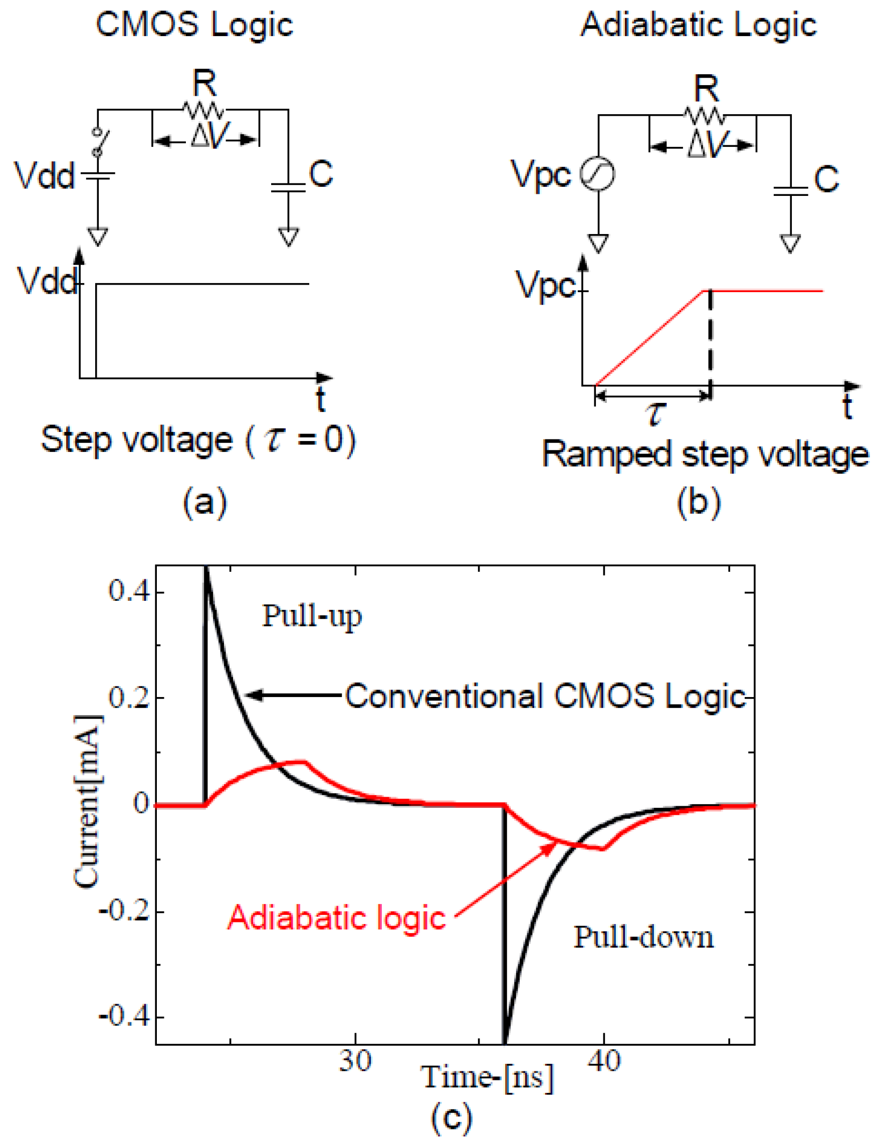
Figure 1. Comparison of the supply current transitions for the equivalent RC models of the (a) CMOS logic step voltage and (b) adiabatic logic ramped step voltage. (c) The peak supply current of the adiabatic logic is significantly lower than that of the conventional CMOS logic under the same parameters and conditions.
Electronics 10 01258 g001
Figure 2. (a) QUALPUF circuit and (b) its timing chart.
Electronics 10 01258 g002
Figure 3. (a) Proposed Adiabatic PUF circuit and (b) its timing chart.
Electronics 10 01258 g003
Figure 4. Proposed adiabatic PUF; (a) active transistors during charging and discharging the response node, (b) RC equivalent model at Cb = 0 V, and (c) RC equivalent model at Cb = 1.8 V.
Electronics 10 01258 g004
Figure 5. Evaluation result of challenge bit under the PMOS transistor body effect. PMOS bulk: tied to source (labeled as BS: body to source), tied to Vpc (labeled as Vpc) and tied to Vdd (labeled as Vdd).
Electronics 10 01258 g005
Figure 6. Proposed 4-bits PUF architecture.
Electronics 10 01258 g006
Figure 7. Input and output signals of the proposed adiabatic PUF.
Electronics 10 01258 g007
Figure 8. PUF cell energy dissipation of the proposed adiabatic PUF versus QUALPUF under the PMOS body effect.
Electronics 10 01258 g008
Figure 9. 4-bits PUF energy dissipation of the proposed adiabatic PUF versus QUALPUF under CMOS process variation.
Electronics 10 01258 g009
Figure 10. Uniqueness of the proposed adiabatic PUF (labeled as Prop.) versus QUALPUF under the TOX variation (4-bit PUF).
Electronics 10 01258 g010
Figure 11. Reliability of the proposed adiabatic PUF (labeled as Prop.) versus QUALPUF under the TOX variation (4-bit PUF).
Electronics 10 01258 g011
Figure 12. Uniqueness of the proposed adiabatic PUF (labeled as Prop.) versus QUALPUF under the VTH variation (4-bit PUF).
Electronics 10 01258 g012
Figure 13. Reliability of the proposed adiabatic PUF (labeled as Prop.) versus QUALPUF under the VTH variation (4-bit PUF).
Electronics 10 01258 g013
Figure 14. Current traces of charging and discharging output nodes when Cb signal at logic “0” level; (a) QUALPUF circuit (refer to Figure 2a), and (b) proposed PUF (refer to Figure 3a).
Electronics 10 01258 g014
Table 1. Simulation conditions.
Power supplyVpc: swing from 0.9–1.8 V trapezoidal clock, fVpc = 100 MH
zVpc-: swing from 0–0.9 V trapezoidal power clock, fVpc- = 100 MHzCb voltage: 1.8 pulse signal, fCb = 10 MHz
Transistor parameter and ratioParameter: 0.18 µm ROHM standard CMOS process
Ratio: W/L = 0.6 µm/0.18 µm for all NMOS and PMOS Transistors
Table 2. Comparison of conventional and proposed adiabatic PUFs (with T = 27 °C and CL = 10 fF, fCb = 10 MHz, and fVpc = 100 MHz).
PUFKumar [29]Takahashi [32]This Work
Year201620192021
TopologyAdiabatic SRAMAdiabatic SRAMAdiabatic SRAM
Transistor-number/bit557
Process (nm)180180180
Start-Up power (µW)3.083.080.47
Energy (fJ/bit/cycle)39.1839.1815.98
Uniqueness (%)40.5047.5849.82
Reliability (%)96.2095.1099.47
Publisher’s Note: MDPI stays neutral with regard to jurisdictional claims in published maps and institutional affiliations.