Article

Design of a Charge Pump Circuit and System with Input Impedance Modulation for a Flexible-Type Thermoelectric Generator with High-Output Impedance

Graduate School of Integrated Science and Technology, Shizuoka University, Hamamatsu 432-8561, Japan
*
Author to whom correspondence should be addressed.
Electronics 2021, 10(10), 1212; https://doi.org/10.3390/electronics10101212
Submission received: 2 April 2021 / Revised: 4 May 2021 / Accepted: 13 May 2021 / Published: 19 May 2021
(This article belongs to the Special Issue Energy Harvesting and Energy Storage Systems)

Abstract

:
This paper describes a charge pump system for a flexible thermoelectric generator (TEG). Even though the TEG has high-output impedance, the system controls the input voltage to keep it higher than the minimum operating voltage by modulating the input impedance of the charge pump using two-phase operation with low- and high-input impedance modes. The average input impedance can be matched with the output impedance of the TEG. How the system can be designed is also described in detail. A design demonstration was performed for the TEG with 400 Ω. The fabricated system was also measured with a flexible-type TEG based on carbon nanotubes. Even with an output impedance of 1.4 kΩ, the system converted thermal energy into electric power of 30 μW at 2.5 V to the following sensor ICs.

1. Introduction

The Internet of Things (IoT) currently is attracting researchers’ attention, which is a system for the interaction of information from things such as sensing edge devices to the cloud and servers via the Internet and vice versa [1]. The maintenance costs to replace batteries can be a large portion of the costs of edge devices. Therefore, it is expected that sensing devices should be battery free based on the energy transducer generating electric power from environmental energy such as sunlight and vibration kinetic energy. A thermoelectric generator (TEG) extracts power from a temperature gradient. The open-circuit voltage VOC of the TEG increases in proportion to the temperature difference between hot and cold heat sources [2]. Bulk-type TEGs [3] have a low output impedance (RTEG) of the order of Ω and are in production together with boost converters. Flexible-type thin film TEGs [4] are expected to have various applications because they can be placed on curved surfaces. A drawback of the flexible-type TEG is the high-output impedance of the order of 10–100 Ω, especially in the case of a small form-factor. Even worse, a low-cost small form-factor TEG generates VOC as low as a few hundred mV. To operate sensor ICs, boost converters are required [5,6,7]. In this research, the design of boost charge pump circuits (CPs) is proposed for a flexible-type TEG with high-output impedance, as illustrated in Figure 1. Such a system is used for heat pipes [8] and wrist watches [9].
To design systems with TEGs and integrated CPs, the circuit area and power conversion efficiency (PCE) are key figures of merit. Table 1 summarizes the key features of existing designs and this work. In [10], the design of low-voltage CPs was developed to strike a balance between the circuit area and power efficiency under the conditions of a given output voltage and current. In this design, CPs are driven by voltage sources with zero impedance, while TEGs have a finite output impedance. In [11], both TEGs and CPs were optimally designed to minimize their areas when CPs were driven by TEGs. However, design constraints such as temperature differences and the number of TEG units connected in parallel and in series were not taken into consideration. A design methodology was proposed when VOC and RTEG were given in [12,13]. In [12], an optimum design was provided to determine the dimensions of switching devices and the clock frequency to maximize the output power of the CP when the number of stages N and stage capacitors C of the CP and the VOC and RTEG of TEG were given. However, the output voltage of the CP was not given, whereas the input voltage of the load circuit must be controlled with a specific voltage. In [13], how the input voltage of the CP or the output voltage of the TEG is determined theoretically was discussed when the circuit area of the CP was minimized or, in other words, when the output power of the CP was maximized with a given CP circuit area to generate a target output current at a specific output voltage, as shown in Figure 2a, which is the same target design of this work. However, the minimum operation voltage of circuits was not considered in [13], but it was assumed that the input voltage of the CP can be set at any voltage. Furthermore, no control circuit was disclosed to control the input voltage of the CP in [13]. In this work, the minimum operating voltage of the circuits was taken into consideration in the design, as shown in Figure 2b. This can be a key design point especially for TEGs with a high-output impedance, which have a potentially large IR drop at VDD.
This paper is an extended version of a conference paper [14] to describe its details. A control circuit to operate the CP was proposed to meet the demand that the output current be generated as high as the target current at a specific voltage while the input voltage of the CP is controlled at a voltage higher than the minimum operating voltage. The designs of the CP system and building blocks are presented in Section 2.1 and Section 2.2, respectively, to discuss how the circuits can be optimally designed. The entire system was fabricated in 65 nm CMOS. Experimental results are shown in Section 2.3, and Section 3 gives a summary of this work.

2. Circuit Design

2.1. System Design

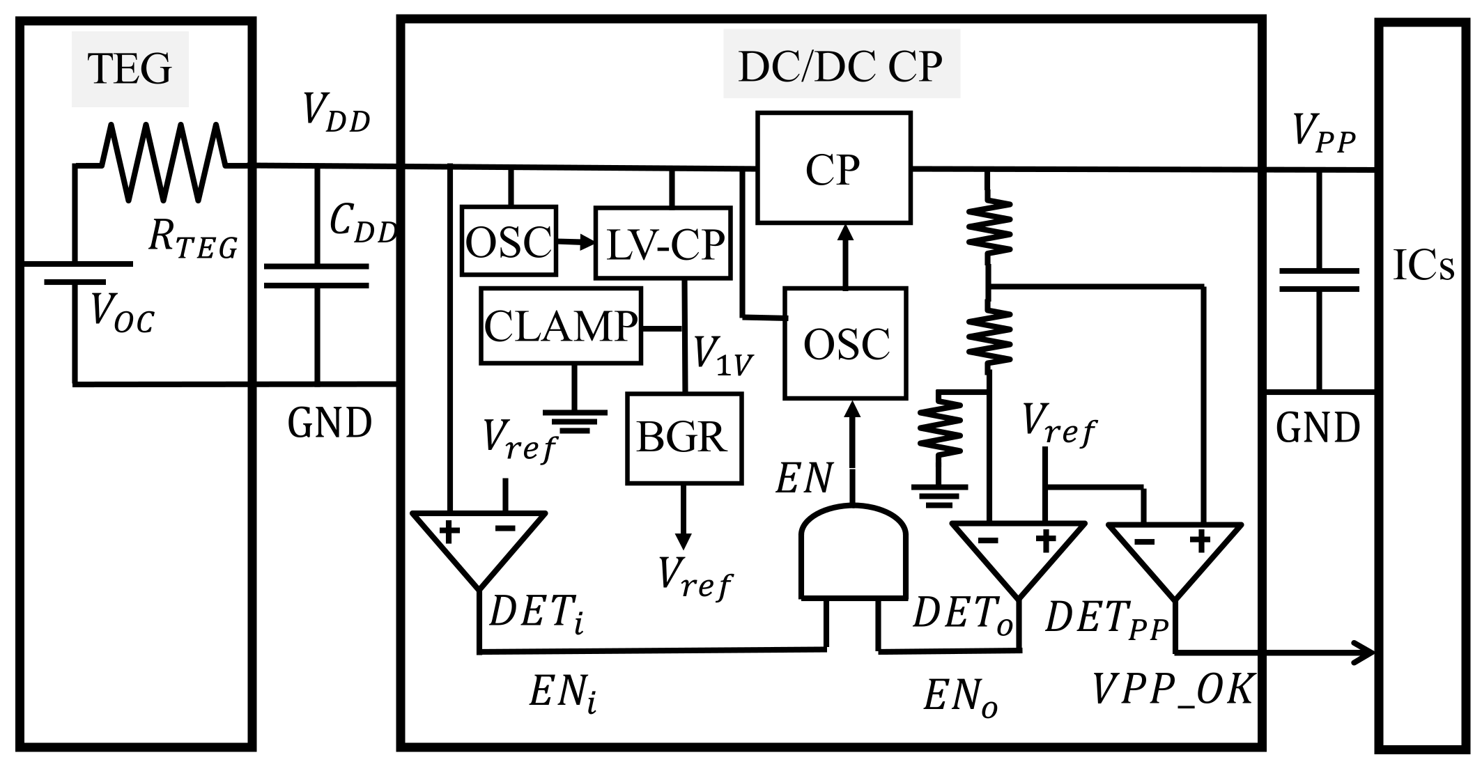
Figure 3 illustrates the proposed CP system to extract power from the TEG with high-output impedance and to drive the following sensor ICs. Table 2 shows the condition to resume or suspend CP operation. A detector DETi monitors VDD and outputs ENi. A detector DETo monitors VPP and outputs ENo. Only when both signals become high, an oscillator OSC outputs a clock to drive the CP. Otherwise, the OSC stops working to not drive the CP. The third detector DETpp generates a signal VPP_OK to let the sensor ICs know the supply voltage is sufficiently high to work.
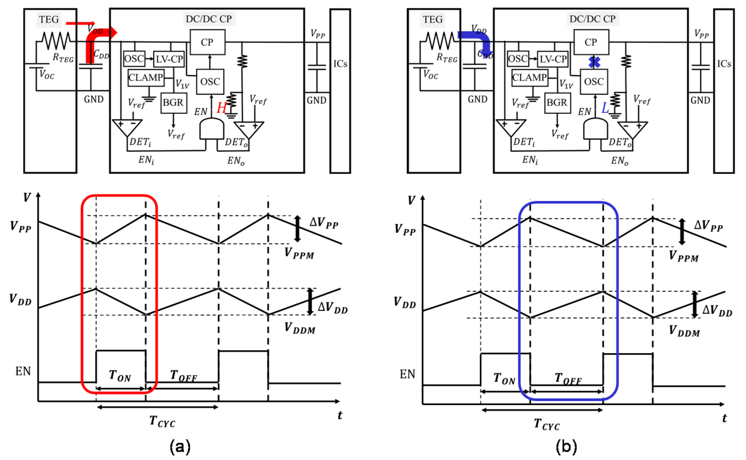
Figure 4 shows two operation phases in steady state. In Phase (a), the CP inputs the current mainly from CDD. Even though RTEG is much larger than the input impedance of CP, VDD can be controlled to be higher than VDD_MIN. Phase (a) starts with EN high when VPP hits VPPM = VPPT, where VPPM and VPPT are the minimum voltage of VPP and the target voltage of VPP, respectively. VPP increases while VDD decreases due to CP operation. EN goes low when (1) ENo goes low or (2) ENi goes low. In the case of (1), the ripple △VPP is determined by the loop response from the output node of the CP to EN. VDDM must be higher than VDDT. In the case of (2), VDDM is equal to VDDT. In Phase (b), VDD increases with the charging current from the TEG, while VPP decreases with the discharging load current. The input impedance of the CP becomes very large because the main charge pump CP is suspended with EN low, even though a small amount of current flows into small building blocks such as LV-CP. Thus, even though the TEG has high-output impedance, the system controls the input voltage to keep it higher than the minimum operating voltage by modulating the input impedance of the charge pump using two-phase operation with low- and high-input impedance modes. The average input impedance can be matched with the output impedance of the TEG. On the other hand, such an operation is not required when the output impedance of TEGs such as the bulk-type is much lower than the input impedance of the CP in operation. The operating point approaches VOC, but the system can work as long as VOC is higher than the minimum operating voltage.
The following equations hold among TON, TOFF, ΔVPP and ΔVDD, where it is assumed that IPP and IDD are the steady-state currents and can be treated as constant when ΔVPP << VPP, ΔVDD << VDD, and ITEG << IDD.
T O N = C D D   Δ V D D I D D = C P P   Δ V P P I P P I L O A D
T O F F = R T E G C D D   ln V O C V D D M V O C V D D M Δ V D D = C P P   Δ V P P I L O A D
IPP and ILOAD are related as Equation (3).
I L O A D = T O N T I P P
When one can regard ITEG as constant in the case of ΔVDD << VDD, IDD and ITEG are related as Equation (4).
I T E G = T O N T I D D

2.2. Building Blocks’ Design

B1: Main charge pump
The given design parameters are the minimum open-circuit voltage of the TEG (VOCMIN), RTEG, VPPT. The number of stages N was designed to maximize IPP at VPPT when the circuit area is given. Based on [15], N is given by Equation (5).
N = 1.7 × N M I N = 1.7 × V P P V D D + V T H E F F V D D / 1 + α T V T H E F F ,
where [x] indicates the floor function of x, NMIN is the minimum number of stages to barely generate VPP, and V T H E F F is an effective threshold voltage of switching transistors, which were called ultra-low power diodes in [16]. The capacitance of each stage capacitor C is related with IPP and IDD as Equations (6) and (7), where the clock frequency f is determined to maximize IPP.
I P P = f C 1 + α T N N 1 + α T + 1 V D D N + 1 V T H E F F V P P ,
I D D = N 1 + α T + 1 I P P + α T 1 + α T + α B f N C V D D + I C T R L ,
where αT and αB are the ratios of the top (CTOP) and bottom plate parasitic capacitance (CBTM) to C, CTOP/C and CBTM/C, respectively. Note that CBTM includes the parasitic capacitance of an oscillator to drive the main CP. ICTRL is the input current for the control circuits, which was assumed to be βIDD using the design parameter β (<1) in this paper because the auxiliary circuits assumed in this paper as shown later steadily ran regardless of TON. IDD is also given by Equation (8) at the extreme case of TON = T and TOFF = 0.
I D D = V O C V D D R T E G
From Equations (6)–(8), the minimum C needs to meet Equation (9).
C = 1 β N V O C V D D f R T E G N + 1 + α T N 1 + α T + 1 V D D N + 1 V T H E F F V P P + α T 1 + α T + α B N 2 V D D
To have a duty ratio of TON/T smaller than a factor of γ, the C to be designed must be increased by a factor of 1/γ.
The parameters shown in Table 3 were used for design demonstration. VDDMIN was mainly determined by the technology used to design, e.g., the availability of low-Vt CMOS and circuits used in the system. As will be shown later, it was limited by an oscillator to generate a clock with 10 MHz. Such a moderate frequency was required to have a sufficiently small circuit system built in the same sensor ICs. From Equations (5) and (9), N and C were calculated to be 19 and 4.8 pF at VDDT = 0.5 V, respectively. Figure 5 shows PPP and CP area NC/γ as a function of VDD.
B2: Auxiliary circuits
As illustrated in Figure 3, the detectors compare VDD and VPP with a reference voltage VREF generated by bandgap reference BGR [17]. To provide a supply voltage V1V~1 V to the BGR, another small CP (LV-CP) was implemented. The LV-CP is operated in open loop not to affect the VDDMIN of the system. A dedicated oscillator starts running without any input signal other than VDD. When LV-CP converts power to the output terminal and V1V reaches about 1 V, a clamping circuit CLAMP with NMOSFETs connected in series with the output terminal clamps the output voltage. V1V is also used as the supply voltage of all the logic gates and the detectors. Figure 6 shows a simulated result of the BGR. VREF is saturated when V1V > 0.8 V.

2.3. Experimental Results

The system was designed in 65 nm low-Vt CMOS technology, as shown in Figure 7. The entire area was 0.28 μm2. The CPs had an N of 20 and a C of 15 pF. The LV-CP had an N of six and a C of 3 pF to generate the supply current of 10 μA at 1 V, which was sufficiently high for the following circuits while keeping γ < 0.2.
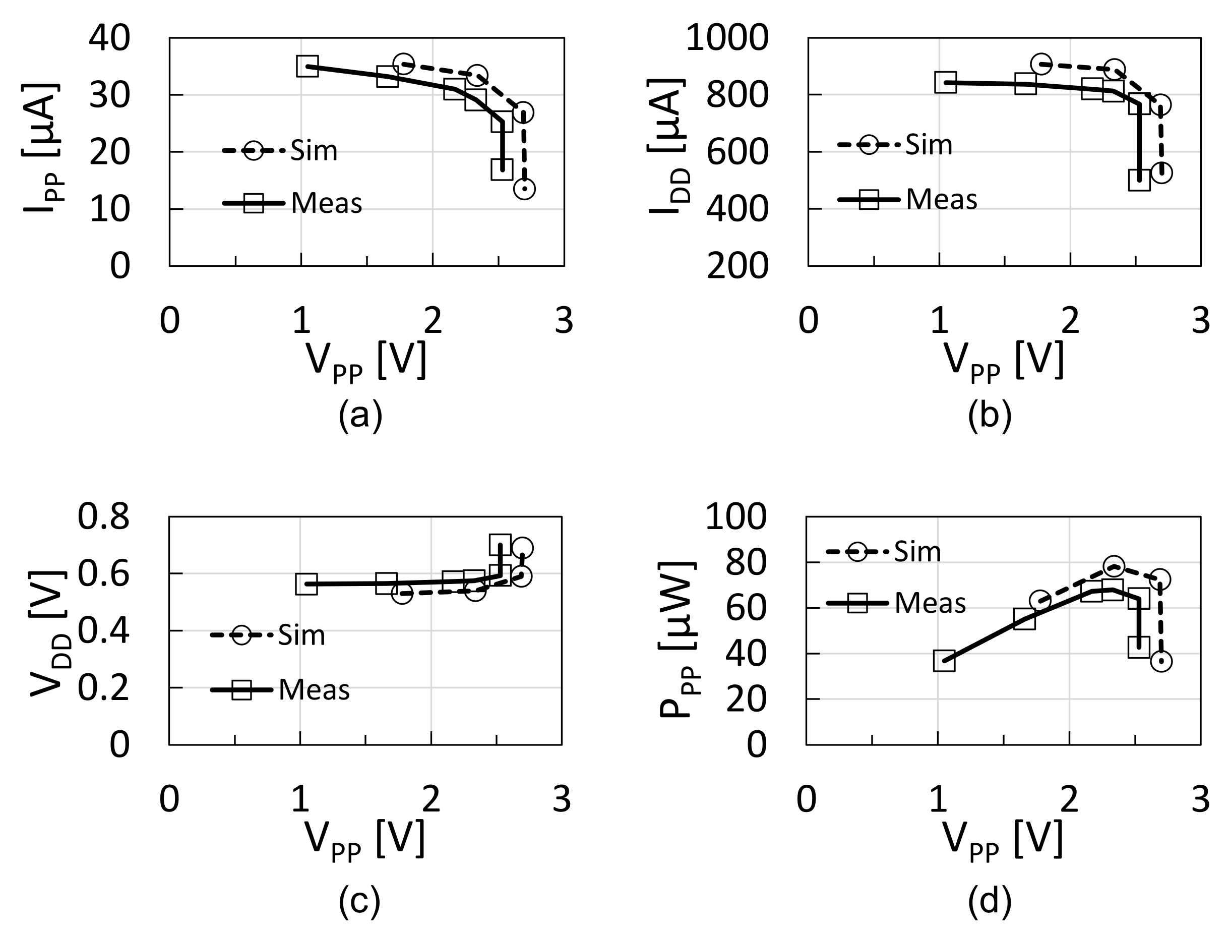
The input terminal was connected to an equivalent circuit of the TEG with VOC and RTEG. A CDD of 300 nF and a CPP of 1 nF were connected to the input and output terminals of the CP system, respectively. Since the system did not work at a VOC of 0.6 V probably because the VTH of MOSFETs was close to the slow corner while the simulation was performed at the typical corner, the experiments were performed at VOC of 0.8 V. Figure 8 shows IPP, IDD, VDD, and PPP as a function of VPP where VPP was varied by varying the load resistance. All the simulations were performed with the slow-corner model. The measured results were matched with the simulated ones with an error of about 10%. VPP was regulated at 2.5 V when IPP was 25 μA or lower. The average VDD was 0.6 V or higher when VPP was regulated.
To see the dynamic response of VPP and VDD against VOC, VOC was made to go up and down between 0.5 V and 1 V in 200 μs, as shown in Figure 9. A signal EN was also monitored using a buffer whose supply voltage was V1V. In the period T1, because VDD was lower than VDDT, EN stayed low. In the period T2, because VDD was higher than VDDT, but VPP was lower than VPPT, EN stayed high. Once VPP reached VPPT, in the period T3, the system stayed in the steady state where the TON/TOFF operation was repeated to keep VPP and VDD at VPPT and VDDT, respectively.
The system was also tested with the TEG using a thermal source, as shown in Figure 10. The TEG was based on carbon nanotubes [18]. The TEG module was built to fit with a pipe, which flowed hot liquid or gas. Because the TEG module had an RTEG of 1.4 kΩ, VOC needed to be set at a higher voltage of 1.1 V with a temperature difference of 66 K to enable the fabricated converter system to be functional, as shown in Figure 11.
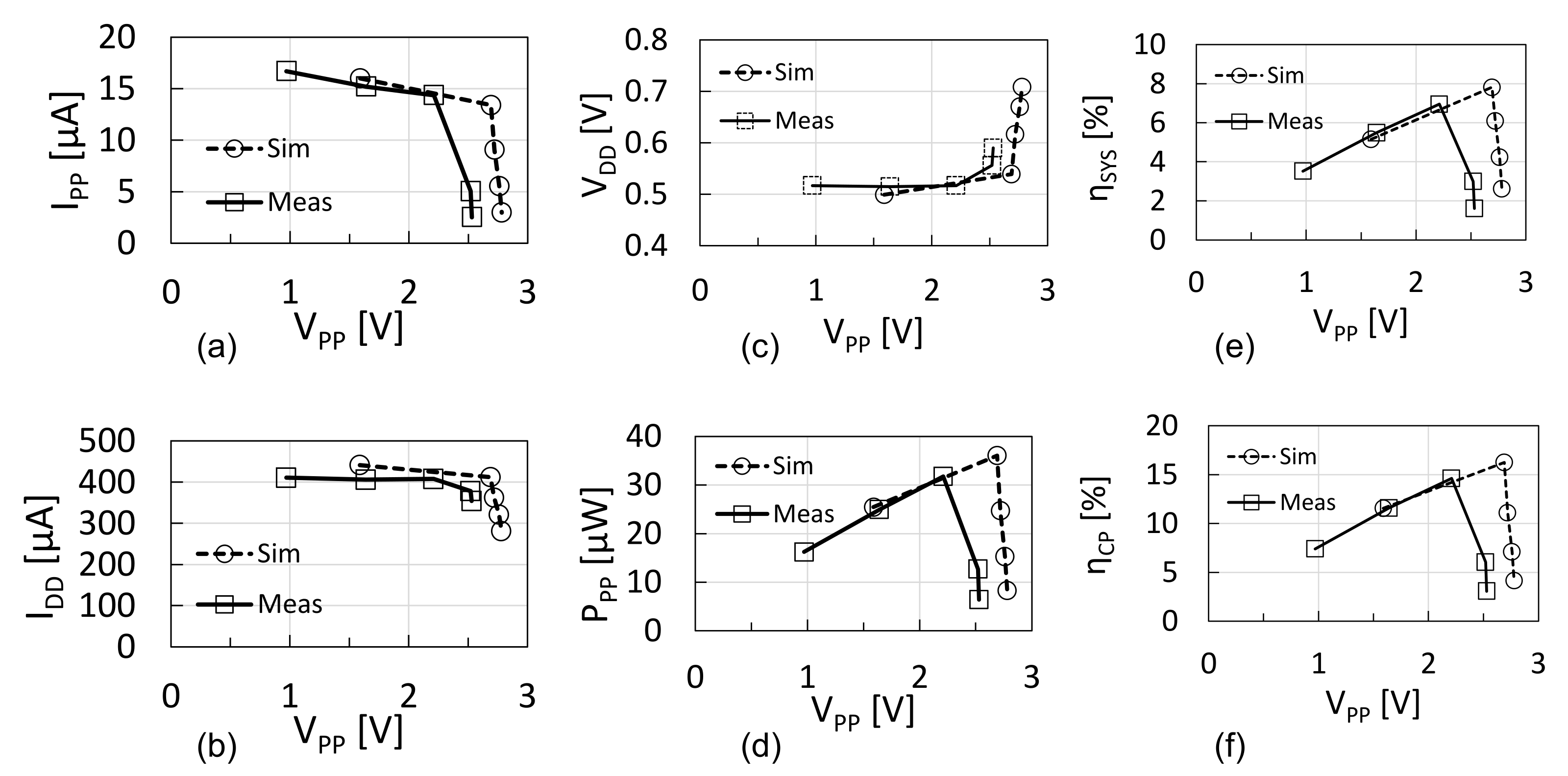
Figure 12 shows IPP, IDD, VDD, PPP, ηSYS, and ηCP as a function of VPP. ηSYS and ηCP are defined by (VPP × IPP)/(VOC × IDD) and (VPP × IPP)/(VDD × IDD), respectively. The VPP regulation point was different by 0.3 V between measured and simulated, but the electric values except for it were in good agreement. It was confirmed that the converter system with the TEG module under the experimental condition could supply power of 30 μW at 2.5 V to the following sensor ICs. The overall power conversion efficiency ηSYS was hit at about 7% against a theoretical limit with no loss of 50%. The power conversion efficiency of the converter system ηCP was 15% when VDD was 0.55 V at VPP of 2.5 V, i.e., a voltage ratio (VPP/VDD) of 4.5. For comparison, ηCP of 20%, 32%, and 45% was realized with a VDD of 0.1 V, 0.2 V, and 0.3 V at a VPP of 0.5 V, respectively, in [10]. Thus, the ηCP of the proposed converter system was a little lower than that of [10] at the voltage ratio of 4.5. The design optimization may need to be improved to increase power conversion efficiency by including the TEG electrical parameters in the design parameters.

3. Conclusions

A charge pump circuit system was presented for energy harvesting based on a flexible-type thermoelectric generator with high-output impedance. Even though the charge pump was operated with a highly resistive TEG, the input voltage could be controlled at a voltage higher than VDDMIN by modulating the input impedance of the CP using two-phase operation with low- and high-input impedance modes. The average input impedance could be matched with the output impedance of TEG. The design methodology was proposed to determine the N and C of the main charge pump when VOC, RTEG, VPP, f, and VDDMIN were given. The system was fabricated in 65 nm CMOS to demonstrate the functionality of the system with the TEG. Using an equivalent circuit for the TEG, the system was validated with a VOC of 0.8 V and an RTEG of 400 Ω. VPP regulation was successfully observed. The circuit system was also measured with a flexible-type TEG and a thermal source. The system converted thermal energy into power to 30 μW at 2.5 V. By adding a full-bridge rectifier between the energy transducer and the proposed converter, the control circuit would be able to work even with other energy transducers such as piezoelectric or electrostatic vibration energy transducers with an AC equivalent voltage source and high-output impedance.

Author Contributions

Conceptualization, T.T.; methodology, K.K. and T.T.; software, K.K.; validation, K.K. and T.T.; formal analysis, K.K. and T.T.; investigation, K.K. and T.T.; writing—original draft preparation, K.K.; writing—review and editing, T.T.; funding acquisition, T.T. All authors have read and agreed to the published version of the manuscript.

Funding

This research was partially funded by Zeon Corp. and Micron Foundation.

Acknowledgments

This work was supported by Zeon Corp., VDEC, Synopsys, Inc., Cadence Design Systems, Inc. Rohm Corp., and Micron Foundation. The authors wish to thank M. Futagawa and H. Hirano and S. Ota for technical discussions.

Conflicts of Interest

The authors declare no conflict of interest.

Nomenclature

CCapacitance per stage
CDDCapacitor connected to VDD
CPPCapacitor connected to VPP
fClock frequency
ICPInput current of CP
ICTRLInput current of control circuits
IDDOperating current of the TEG and CP
ILOADLoad current of the CP
ITEGOutput current of the TEG
NStage number of the CP
PDDInput power of the CP
PPPOutput power of the CP
PTEGGenerated power of the TEG
αTRatio of top plate capacitance to C
αBRatio of bottom plate capacitance to C
RTEGOutput impedance of the TEG
TOperation period, TON + TOFF
TOFFSuspended period
TONResumed period
VDDInput voltage of the CP
VDDTTarget input voltage of the CP to be controlled
VDDMMinimum VDD in operation
ΔVDDRipple in VDD
VPPOutput voltage of the CP
VPPTTarget output voltage of the CP to be controlled
VPPMMinimum VPP in operation
ΔVPPRipple in VPP
βRatio of ICTRL to IDD
γOperation duty; TON/T

References

  1. Lu, C.; Raghunathan, V.; Roy, K. Efficient Design of Micro-Scale Energy Harvesting Systems. IEEE J. Emerg. Sel. Top. Circuits Syst. 2011, 1, 254–266. [Google Scholar] [CrossRef]
  2. Huesgen, T.; Woias, P.; Kockmann, N. Design and fabrication of MEMS thermoelectric generators with high temperature efficiency. Sens. Actuators A Phys. 2008, 145, 423–429. [Google Scholar] [CrossRef]
  3. Date Sheet of TGP-651, Micropelt. Available online: http://www.micropelt.com/ (accessed on 2 April 2021).
  4. Du, Y.; Xu, J.; Paul, B.; Eklund, P. Flexible thermoelectric materials and devices. Appl. Mater. Today 2018, 12, 366–388. [Google Scholar] [CrossRef]
  5. Priya, S.; Inman, D.J. Chapter 18: Energy Harvesting for Active RF Sensors and ID Tags. In Energy Harvesting Technologies; Springer: New York, NY, USA, 2009. [Google Scholar]
  6. Li, Y.; Buddharaju, K.; Singh, N.; Lo, G.Q.; Lee, S.J. Chip-Level Thermoelectric Power Generators Based on High-Density Silicon Nanowire Array Prepared with Top-Down CMOS Technology. IEEE Electron Device Lett. 2011, 32, 674–676. [Google Scholar] [CrossRef]
  7. Shrivastava, A.; Wentzloff, D.; Calhoun, B.H. A 10mV-input boost converter with inductor peak current control and zero detection for thermoelectric energy harvesting. In Proceedings of the IEEE 2014 Custom Integrated Circuits Conference, San Jose, CA, USA, 15–17 September 2014. [Google Scholar] [CrossRef]
  8. Remeli, M.F.; Kiatbodin, L.; Singh, B.; Verojporn, K.; Date, A.; Akbarzadeh, A. Power Generation from Waste Heat Using Heat Pipe and Thermoelectric Generator. Energy Procedia 2015, 75, 645–650. [Google Scholar] [CrossRef] [Green Version]
  9. Priya, S.; Inman, D.J. Chapter 11: Thermoelectric Energy Harvesting. In Energy Harvesting Technologies; Springer: New York, NY, USA, 2009. [Google Scholar]
  10. Tokuda, S.; Tanzawa, T. Toward a Minimum-Operating-Voltage Design of DC-DC Charge Pump Circuits for Energy Harvesting. In Proceedings of the 2019 IEEE International Symposium on Circuits and Systems (ISCAS), Sapporo, Japan, 26–29 May 2019; pp. 1–4. [Google Scholar] [CrossRef]
  11. Koketsu, K.; Tanzawa, T. An Optimum Design of Thermal Energy Transducers and Power Converters for Small Form-Factor Thermoelectric Energy Harvester. In Proceedings of the IEICE General Conference, Tokyo, Japan, 19–22 March 2019; Available online: http://hdl.handle.net/10297/00026345 (accessed on 27 March 2019).
  12. Lu, C.; Park, S.P.; Raghunathan, V.; Roy, K. Analysis and Design of Ultra Low Power Thermoelectric Energy Harvesting Systems. In Proceedings of the 16th ACM/IEEE International Symposium on Low-Power Electronics and Design, Austin, TX, USA, 11 October 2010; pp. 183–188. [Google Scholar] [CrossRef]
  13. Tanzawa, T. Design of DC-DC Switched-Capacitor Voltage Multiplier driven by DC Energy Transducer. In Proceedings of the 2014 21st IEEE International Conference on Electronics Circuits and Systems, Marseille, France, 7–10 December 2014; pp. 327–330. [Google Scholar] [CrossRef]
  14. Koketsu, K.; Tanzawa, T. A Design of Cold Start Charge Pump for Flexible Thermoelectric Generator with High Output Impedance. In Proceedings of the 2020 27th IEEE International Conference on Electronics, Circuits and Systems, Glasgow, UK, 23–25 November 2020. [Google Scholar] [CrossRef]
  15. Tanzawa, T. An Optimum Design for Integrated Switched-Capacitor Dickson Charge Pump Multipliers with Area Power Balance. IEEE Trans. Power Electron. 2014, 29, 534–538. [Google Scholar] [CrossRef]
  16. Haddad, P.-A.; Gosset, G.; Raskin, J.-P.; Flandre, D. Automated Design of a 13.56 MHz 19 µW Passive Rectifier With 72% Efficiency Under 10 µA load. IEEE J. Solid-State Circuits 2016, 51, 1290–1301. [Google Scholar] [CrossRef]
  17. Banba, H.; Shiga, H.; Umezawa, A.; Miyaba, T.; Tanzawa, T.; Atsumi, S.; Sakui, K. A CMOS bandgap reference circuit with sub-1-V operation. IEEE J. Solid-State Circuits 1999, 34, 670–674. [Google Scholar] [CrossRef] [Green Version]
  18. Suemori, K.; Hoshino, S.; Kamata, T. Flexible and lightweight thermoelectric generators composed of carbon nanotube—Polystyrene composites printed on film substrate. Appl. Phys. Lett. 2013, 103, 153902. [Google Scholar] [CrossRef]
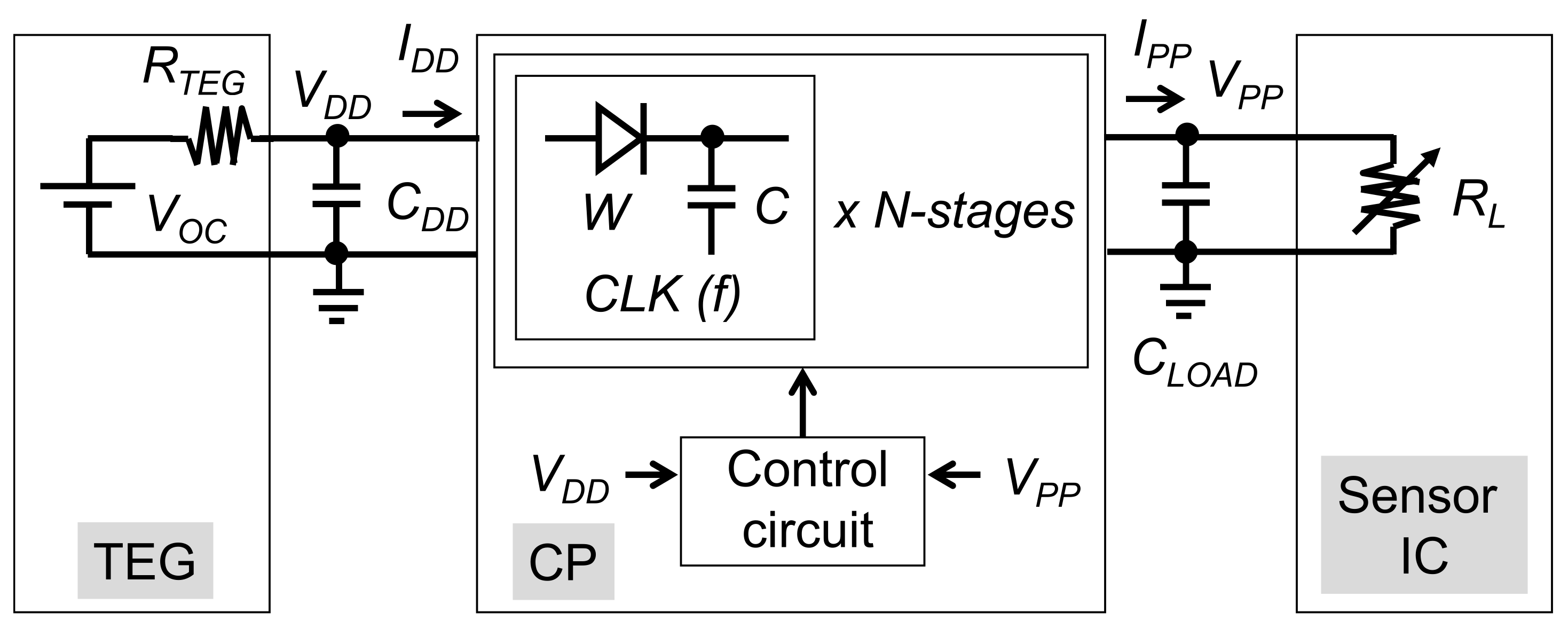
Figure 1. Block diagram of the energy harvesting system based on the TEG and CP.
Electronics 10 01212 g001
Figure 2. Operating points of [8] (a) and of this work (b).
Electronics 10 01212 g002
Figure 3. Building blocks of the proposed CP circuit system.
Electronics 10 01212 g003
Figure 4. Two phases of the circuit operation. (a) Low and (b) high input impedance modes
Electronics 10 01212 g004
Figure 5. (a) PPP vs. VDD; (b) CP area NC/γ vs. VDD.
Electronics 10 01212 g005
Figure 6. VREF vs. VDD.
Electronics 10 01212 g006
Figure 7. Die photo.
Electronics 10 01212 g007
Figure 8. (a) IPP, (b) IDD, (c) VDD, and (d) PPP as a function of VPP.
Electronics 10 01212 g008
Figure 9. Dynamic behavior of VPP and VDD against VOC.
Electronics 10 01212 g009
Figure 10. The TEG module (a) and experimental setup with the TEG (b).
Electronics 10 01212 g010
Figure 11. VOC vs. ΔT (a) and IDD vs. VDD at ΔT of 66 K (b).
Electronics 10 01212 g011
Figure 12. (a) IPP, (b) IDD, (c) VDD, (d) PPP, (e) ηSYS, and (f) ηCP as a function of VPP.
Electronics 10 01212 g012
Table 1. Comparison of the key features of this work with existing designs.
Optimum Design TargetGiven Design ParametersParameter to Be OptimizedParameters to Be Determined
Tokuda [10]CPVPP, IPP, VDD, fArea of the CP to be minimized and the PCE to be maximized N ,   C
Koketsu [11]TEG + CPVPP, IPP, fArea of the TEG and CP to be minimizedVOC, RTEG, N, C
Lu [12]VOC, RTEG, N, CPPP to be maximizedW, f
Tanzawa [13]VOC, RTEG, VPP, fIPP @ VPP to be maximized N ,   C
This workVOC, RTEG, VPP ,   f , VDDMIN
Table 2. Operation condition of the main CP against VDD and VPP.
VPP < VPPTVPP > VPPT
VDD > VDDTResumeSuspend
VDD < VDDTSuspendSuspend
Table 3. Design parameters used in this work.
VDDMINVDDTVTHEFFVPPTRTEGVOCMINfαTαBβγ
0.45 V0.5 V0.25 V2.5 V400 Ω0.6 V10 MHz0.10.20.20.33
Publisher’s Note: MDPI stays neutral with regard to jurisdictional claims in published maps and institutional affiliations.