
A Fully Integrated AC-DC Converter in 1 V CMOS for Electrostatic Vibration Energy Transducer with an Open Circuit Voltage of 10 V

Abstract
:1. Introduction
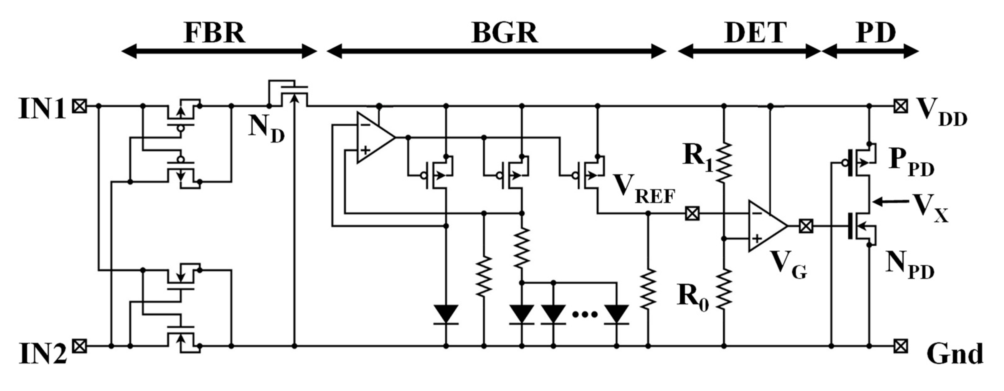
2. Circuit Design
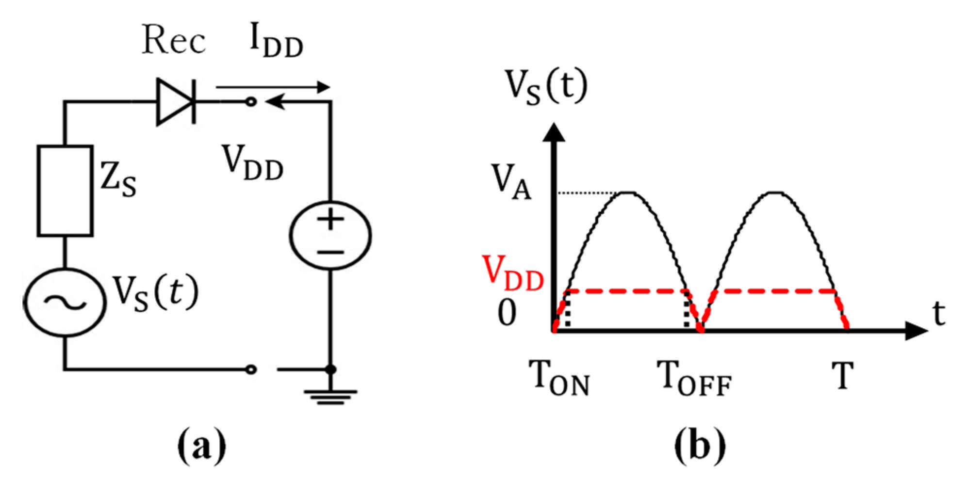
2.1. System Design
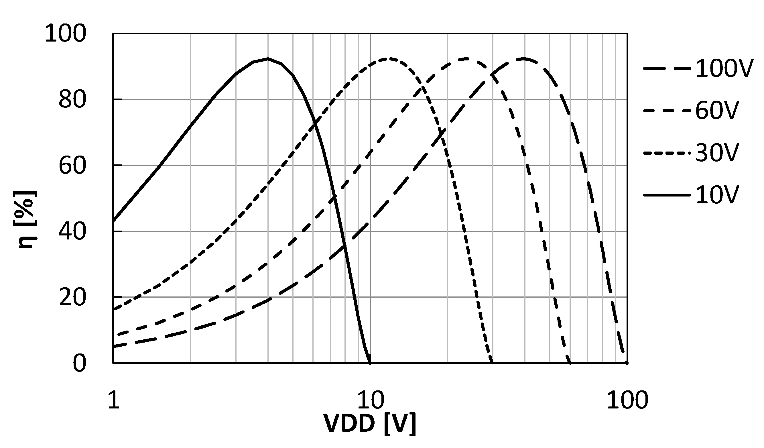
2.2. Power Comversion Efficiency
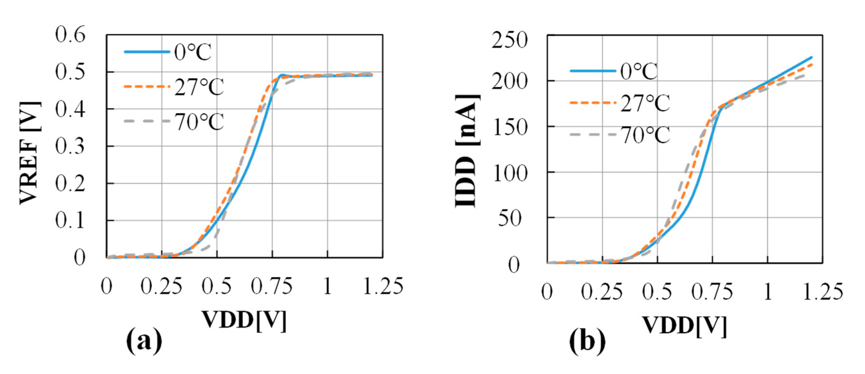
2.3. Bandgap Reference (BGR)
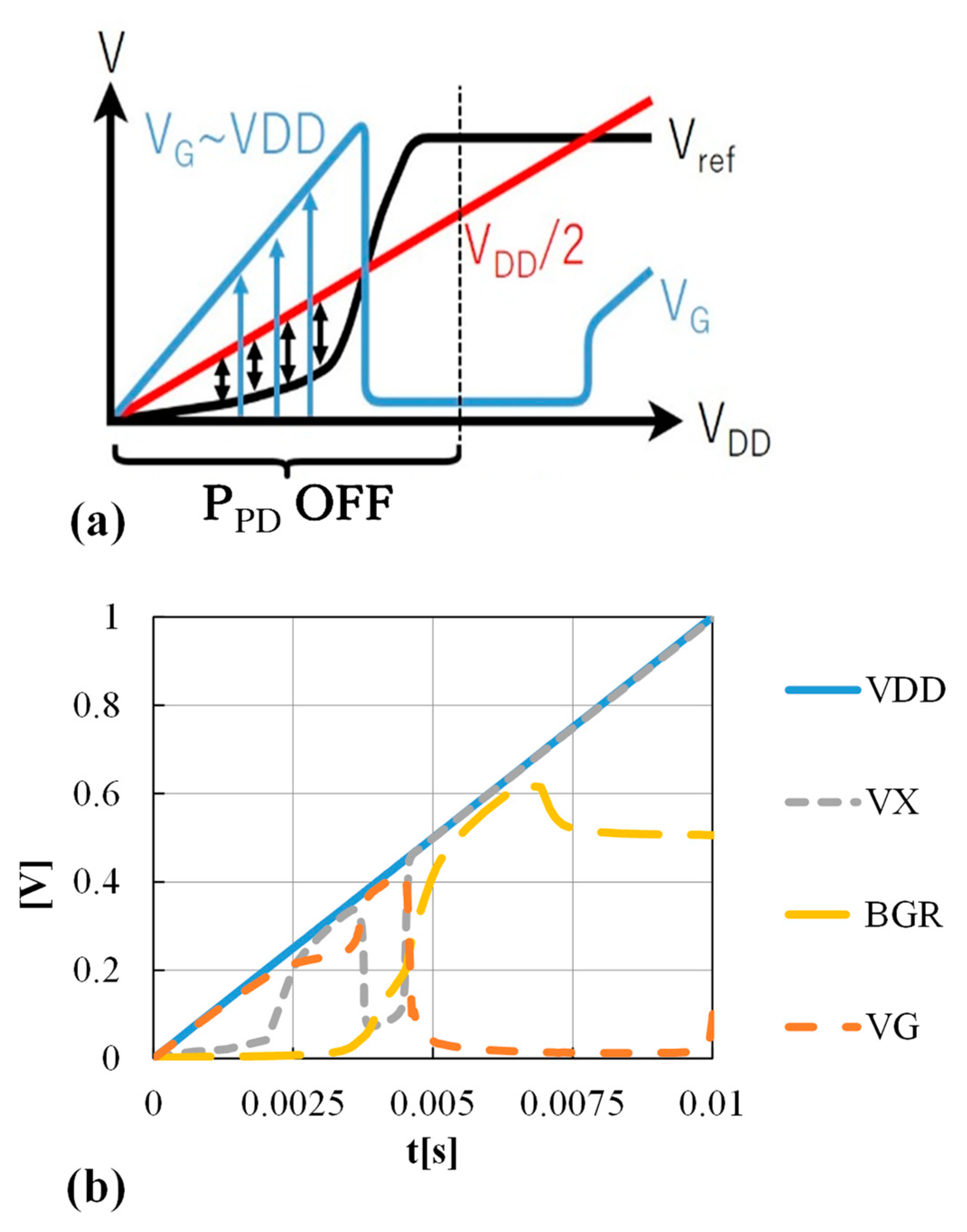
2.4. Built-In Power-On Reset (POR)
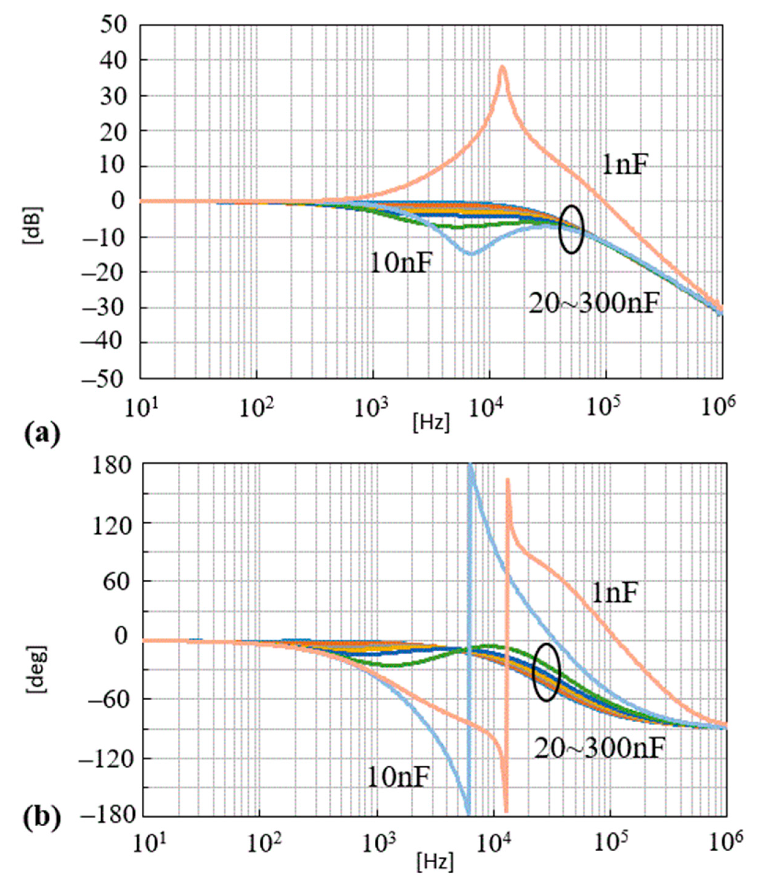
2.5. Decoupling Capacitor
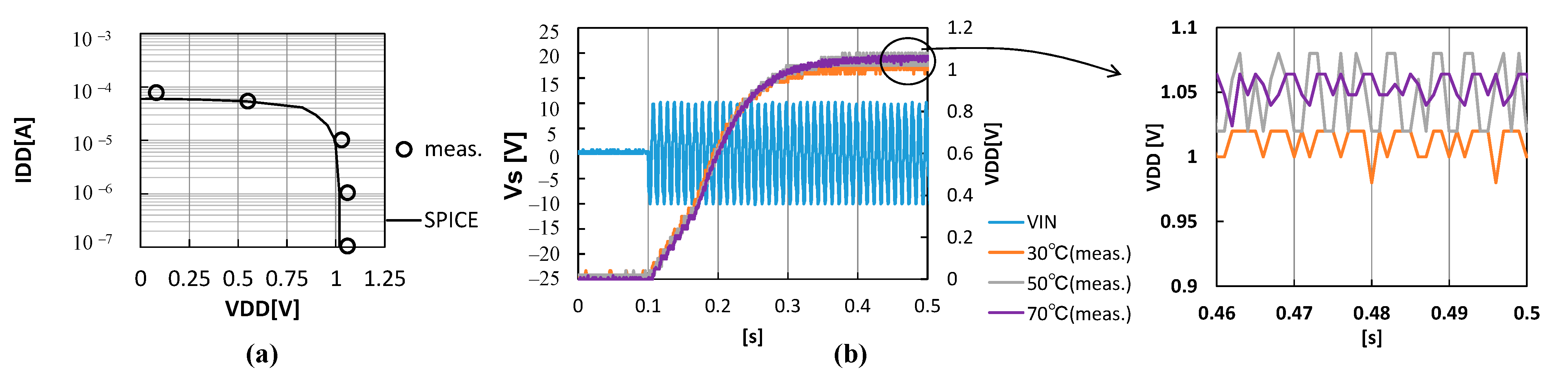
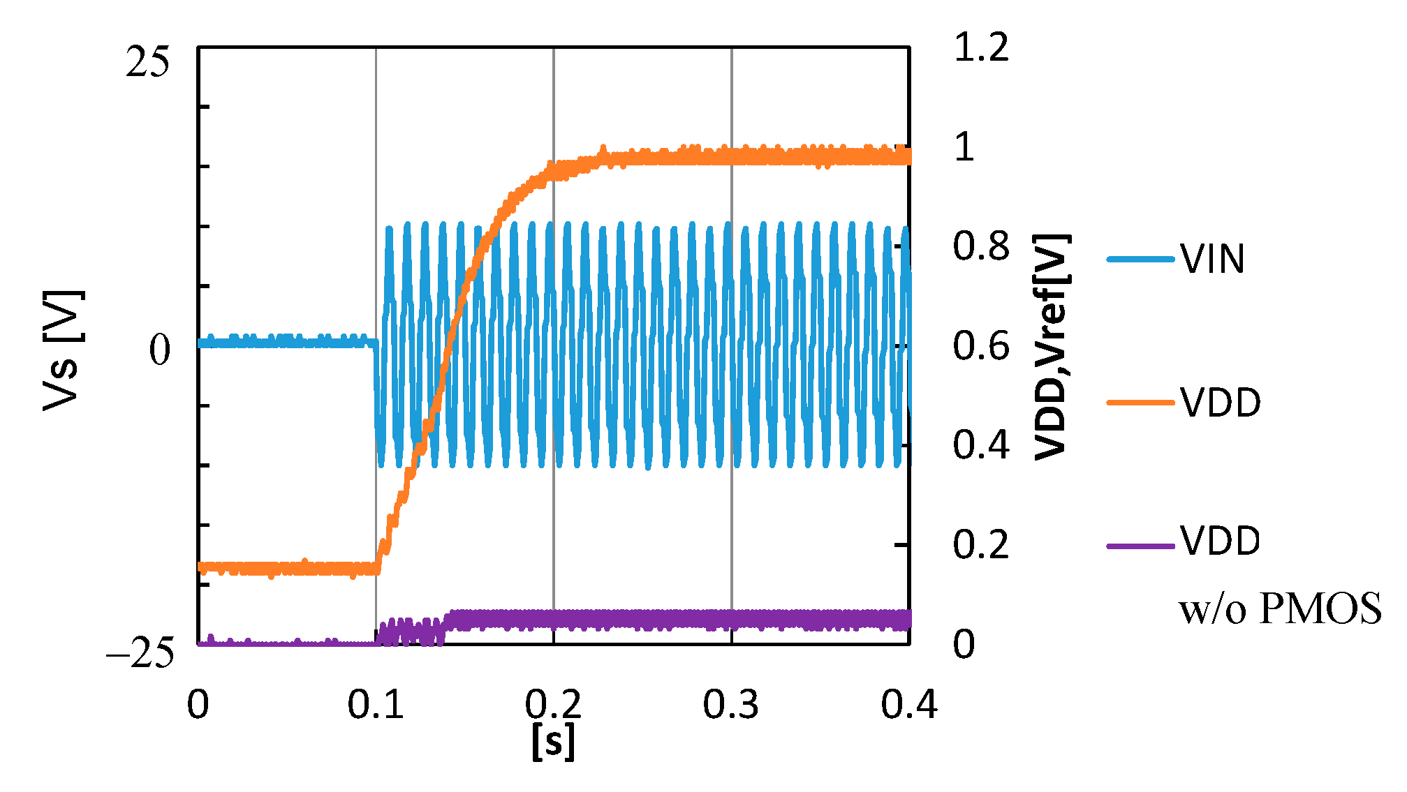
3. Experiments
4. Discussions
4.1. Comparison with Previously Reported Converters
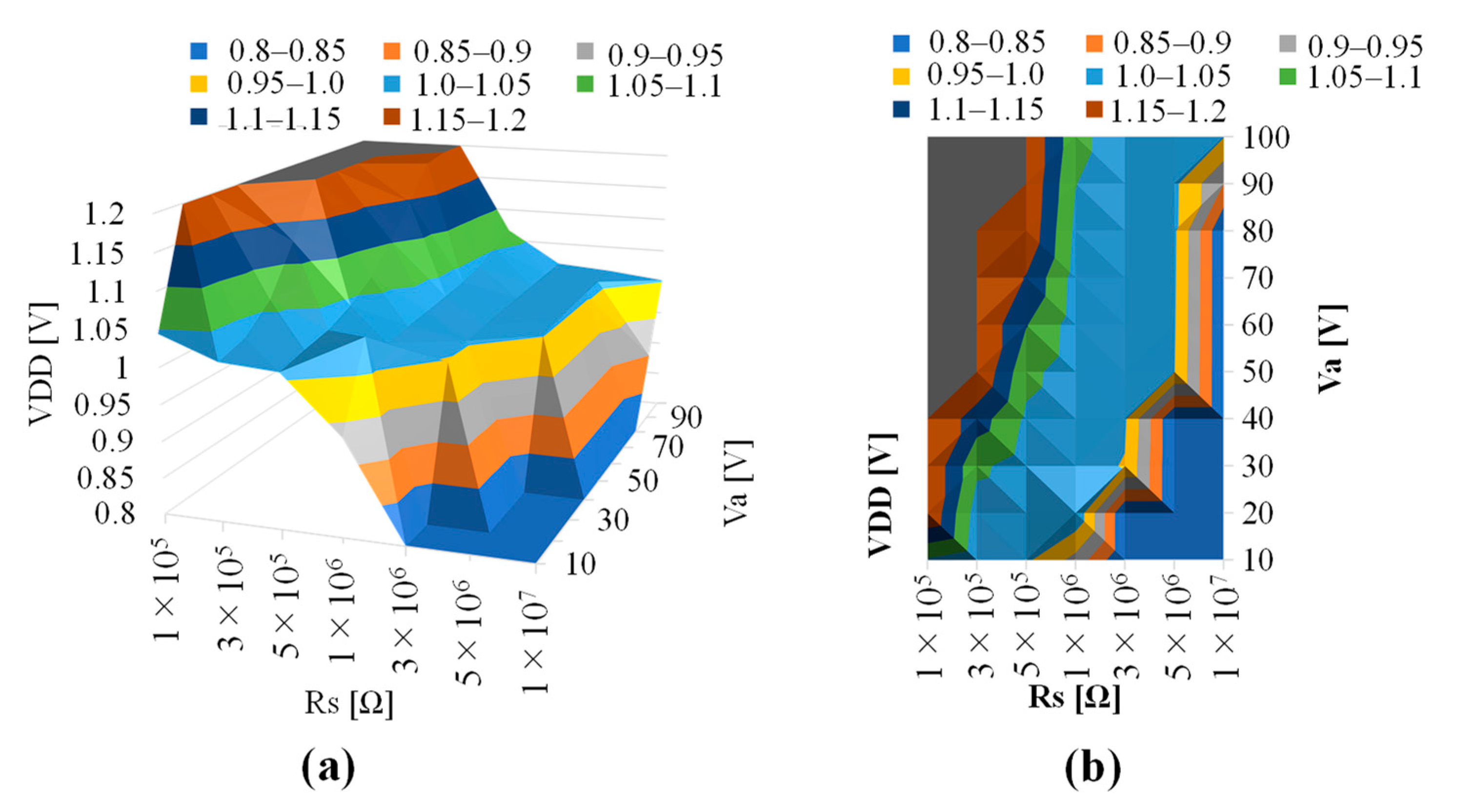
4.2. Limination of the Proposed Converter on VA and RS of ES-EH
5. Conclusions
Author Contributions
Funding
Acknowledgments
Conflicts of Interest
References
- Kazmiersuki, T.; Beedy, S. Energy Harvesting Systems: Principles, Modeling and Applications; Springer: Berlin/Heidelberg, Germany, 2010; pp. 1–78. [Google Scholar]
- Fu, Q.; Suzuki, Y.; Suzuki, Y. MEMS vibration electret energy harvester with combined electrodes. In Proceedings of the 2014 IEEE 27th International Conference on Micro Electro Mechanical Systems (MEMS), San Francisco, CA, USA, 26–30 January 2014; pp. 409–412. [Google Scholar] [CrossRef]
- Hashiguchi, G. Electromechanical theory of microelectromechanical devices. IEICE Electron. Express 2014, 11, 20142007. [Google Scholar] [CrossRef] [Green Version]
- De Queiroz, A.C.M.; Domingues, M. The Doubler of Electricity Used as Battery Charger. IEEE Trans. Circuits Syst. II Express Briefs 2011, 58, 797–801. [Google Scholar] [CrossRef]
- Stanzione, S.; Van Liempd, C.; Van Schaijk, R.; Naito, Y.; Yazicioglu, R.F.; Van Hoof, C. A self-biased 5-to-60 V input voltage and 25-to-1600 µW integrated DC-DC buck converter with fully analog MPPT algorithm reaching up to 88% end-to-end efficiency. In Proceedings of the 2013 IEEE International Solid-State Circuits Conference Digest of Technical Papers, San Francisco, CA, USA, 17–21 February 2013; IEEE: Piscataway, NJ, USA, 2013; pp. 74–75. [Google Scholar]
- Stanzione, S.; Van Liempd, C.; Nabeto, M.; Yazicioglu, F.R.; Van Hoof, C. 20.8 A 500 nW batteryless integrated electrostatic energy harvester interface based on a DC-DC converter with 60 V maximum input voltage and operating from 1 μW available power, including MPPT and cold start. In Proceedings of the 2015 IEEE International Solid-State Circuits Conference—(ISSCC) Digest of Technical Papers, San Francisco, CA, USA, 22–26 February 2015; IEEE: Piscataway, NJ, USA, 2015; pp. 1–3. [Google Scholar]
- Peters, C.; Kessling, O.; Henrici, F.; Ortmanns, M.; Manoli, Y. CMOS Integrated Highly Efficient Full Wave Rectifier. In Proceedings of the 2007 IEEE International Symposium on Circuits and Systems, Los Alamitos, CA, USA, 27–30 May 2007; IEEE: Piscataway, NJ, USA, 2007; pp. 2415–2418. [Google Scholar]
- Ulusan, H.; Gharehbaghi, K.; Zorlu, O.; Muhtaroglu, A.; Kulah, H. A Fully Integrated and Battery-Free Interface for Low-Voltage Electromagnetic Energy Harvesters. IEEE Trans. Power Electron. 2014, 30, 3712–3719. [Google Scholar] [CrossRef]
- Banba, H.; Shiga, H.; Umezawa, A.; Miyaba, T.; Tanzawa, T.; Atsumi, S.; Sakui, K. A CMOS bandgap reference circuit with sub-1-V operation. IEEE J. Solid-State Circuits 1999, 34, 670–674. [Google Scholar] [CrossRef] [Green Version]
- De Pelecijn, E.; Steyaert, M.S.J. A Fully Integrated Switched-Capacitor-Based AC–DC Converter for a 120 VRMS Mains Interface. IEEE J. Solid-State Circuits 2019, 54, 2009–2018. [Google Scholar] [CrossRef]
- Kawauchi, H.; Tanzawa, T. A Fully Integrated Clocked AC-DC Charge Pump for Mignetostrictive Vibration Energy Harvesting. Electronics 2020, 9, 2194. [Google Scholar] [CrossRef]
- Chen, Z.; Law, M.-K.; Mak, P.-I.; Zeng, X.; Martins, R.P. Piezoelectric Energy-Harvesting Interface Using Split-Phase Flipping-Capacitor Rectifier with Capacitor Reuse for Input Power Adaptation. IEEE J. Solid-State Circuits 2020, 55, 2106–2117. [Google Scholar] [CrossRef]


| VDD[V] | FF | TT | SS |
|---|---|---|---|
| 0 °C | 1.0 | 1.0 | 1.0 |
| 27 °C | 1.0 | 1.0 | 1.0 |
| 70 °C | 0.90 | 1.0 | 1.0 |
| Temp. | VDD |
|---|---|
| 0 °C | 20 mV |
| 27 °C | mV |
| 70 °C | 22 mV |
| Stanzione [6] | De Pelecijn [10] | Kawauchi [11] | Chen [12] | This Work | |
|---|---|---|---|---|---|
| Energy source | ES-EH | AC mains | MR-EH | PZ-EH | ES-EH |
| Voltage conversion: Up or Down? | Down | Down | Up | Up/Down | Down |
| Architecture | FBR and Buck | Cap-div, SC, and FBR | FBR and AC-DC CP | FBR and DC-DC CP | FBR and Shunt |
| External components | FBR (4 diodes)/LCR (1L,1C,2R) | None (except for CVDD) | |||
| CMOS | 0.25 µm 60 V BCD and 3 V CMOS | 0.35 µm 12 V HV-CMOS | 65 nm 1 V low-Vt CMOS | 0.18 µm CMOS | 65 nm 1 V low-Vt CMOS |
| VDD regulation | N. A. | N. A. | No regulation | N. A. | ±5% |
| Control power | 500 nW | 50 nW | 18 µW | 4 µW (*1) | 700 nW |
| Maximum input peak voltage | 60 V | 168 V | 1 V | N. A. | 10 V (measured), 100 V (potentially) |
| Input power | 1 µW–1 mW | 20 µW | 22 µW | N.A. | 1 µW–100 µW |
| Output power | 1 µW–1 mW | 20 µW | 4 µW | 0.5–64 µW | 1 µW–100 µW |
| Power conversion efficiency | 85% | 81% | 23% | 72% (*1) | 43% |
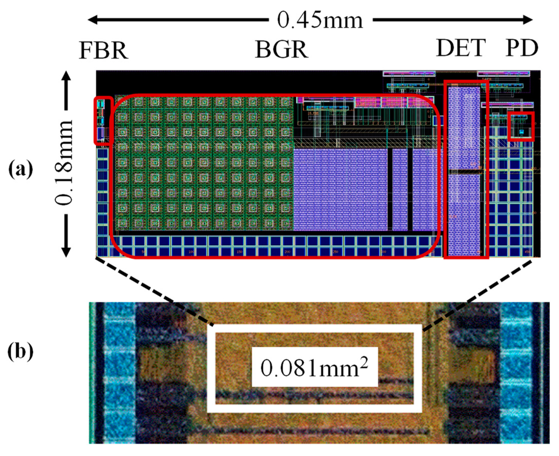
| Die/circuit area | BCD (3 mm2) and CMOS (N.A.) | 9.8 mm2 | 0.11 mm2 | 0.2 mm2 | 0.081 mm2 |
| Area [mm2]/Max. output power [mW] | 4.6 | 612.5 | 27.5 | 3.1 | 8.1 (meas.), 0.81 (sim.) (*2) |
Publisher’s Note: MDPI stays neutral with regard to jurisdictional claims in published maps and institutional affiliations. |
© 2021 by the authors. Licensee MDPI, Basel, Switzerland. This article is an open access article distributed under the terms and conditions of the Creative Commons Attribution (CC BY) license (https://creativecommons.org/licenses/by/4.0/).
Share and Cite
Ishida, Y.; Tanzawa, T. A Fully Integrated AC-DC Converter in 1 V CMOS for Electrostatic Vibration Energy Transducer with an Open Circuit Voltage of 10 V. Electronics 2021, 10, 1185. https://doi.org/10.3390/electronics10101185
Ishida Y, Tanzawa T. A Fully Integrated AC-DC Converter in 1 V CMOS for Electrostatic Vibration Energy Transducer with an Open Circuit Voltage of 10 V. Electronics. 2021; 10(10):1185. https://doi.org/10.3390/electronics10101185
Chicago/Turabian StyleIshida, Yosuke, and Toru Tanzawa. 2021. "A Fully Integrated AC-DC Converter in 1 V CMOS for Electrostatic Vibration Energy Transducer with an Open Circuit Voltage of 10 V" Electronics 10, no. 10: 1185. https://doi.org/10.3390/electronics10101185
APA StyleIshida, Y., & Tanzawa, T. (2021). A Fully Integrated AC-DC Converter in 1 V CMOS for Electrostatic Vibration Energy Transducer with an Open Circuit Voltage of 10 V. Electronics, 10(10), 1185. https://doi.org/10.3390/electronics10101185