Article

Mechanism Analysis of Dynamic On-State Resistance Degradation for a Commercial GaN HEMT Using Double Pulse Test

1
Key Lab for Physical Electronics and Devices, Ministry of Education, Xi’an Jiaotong University, Xi’an 710049, China
2
Institute of Wide Band Gap Semiconductors, School of Electronics and Information Engineering, Xi’an Jiaotong University, Xi’an 710049, China
3
Hangzhou Silan Microelectronics Co., Ltd., Hangzhou 310000, China
*
Authors to whom correspondence should be addressed.
Electronics 2021, 10(10), 1202; https://doi.org/10.3390/electronics10101202
Submission received: 20 April 2021 / Revised: 10 May 2021 / Accepted: 12 May 2021 / Published: 18 May 2021
(This article belongs to the Special Issue GaN-Based Power Electronic Devices and Their Applications)

Abstract

:
The dynamic on-resistance (RON) behavior of one commercial GaN HEMT device with p-GaN gate is investigated under hard-switching conditions. The non-monotonic performance of dynamic RON with off-state voltage ranging from 50 to 400 V is ascribed to the “leaky dielectric” model. The highest normalized RON value of 1.22 appears at 150 and 200 V. The gradual increase and following maximum of dynamic RON are found when the device is exposed to a stress voltage for an extended stress time under 100 and 200 V, which is due to a much longer trapping time compared to detrapping time related to deep acceptors and donors. No obvious RON degradation, thanks to the suppressed trapping effect, is observed at higher VDS. From the multi-pulse test, the dynamic RON is seen to be insensitive to the frequency. It is demonstrated that the leakage, especially under source and drain contact, is a key issue in the dynamic resistance degradation.

1. Introduction

GaN-based power devices, such as high electron mobility transistor (HEMT), are promising in the field of high-frequency, high-power, low-loss converters [1]. Understanding its characteristics is very helpful for better using those devices in power electronics systems. However, the degradation of the dynamic on-state resistance RON after switching from high voltage off state hinders the practical application of these devices. Now, two physical mechanisms have been proposed to explain RON degradation. One is the trapped electrons [2,3] coming from the surface traps between the gate and drain area and/or the buffer traps under the two-dimensional electron gas (2DEG) channel induced by high electric field across the drain-to-substrate in the off state. The other is hot electrons [4,5], generated in the channel, which can be injected to and trapped at the surface or the buffer stack during the high voltage switching transients. Though several advanced device technologies, such as filed plate [6] and optimized buffer design [7], have been performed to release the current collapse, dynamic RON variation is still a big problem for currently commercial GaN devices. Previously, most reports focus on the device level analysis or research for material quality enhancement. In this case, the impact of dynamic on-state resistance should be fully investigated to predict the accurate performance of a GaN converter, and it is better not to use the static RON values for the evaluation of conduction loss.
The double pulse test (DPT) is a widely used methodology to achieve the dynamic RON of the power devices when switching under hard conditions [8,9,10,11,12]. The switching transients of device under test (DUT) can be captured at the second pulse under desired voltage and current. Thus, the rise of junction temperature ascribed to the switching loss can be ignored. The impact on dynamic RON, including off-state time, off-state voltage, drain current, temperature, frequency, duty cycle and gate voltage, can be investigated by using this method. Moreover, DPT results can provide some guidance for converter design, such as switching frequency and dead-time selections, thermal management, and efficiency estimation [13,14]. The impact of gate characteristics [15], off-state voltages [14,16], and continuous operating mode has [17] already been discussed. The off-state time before the first gate pulse is one of the key parameters, which can affect the trapping effect and thus results in uncertainty of the RON value. However, few reports can be found to discuss this issue.
In this paper, the DPT evaluation method was carried out for further understanding of dynamic on-state resistance by investigating the impact of the off-state time before the first gate pulse, the off-state voltage and by the continuous switching operation with two frequencies. The DUT was a commercially purchased GaN normally-off device with a p-type GaN gate from GaN System (GS66504B [18]) with the typical RON of 100 mΩ.

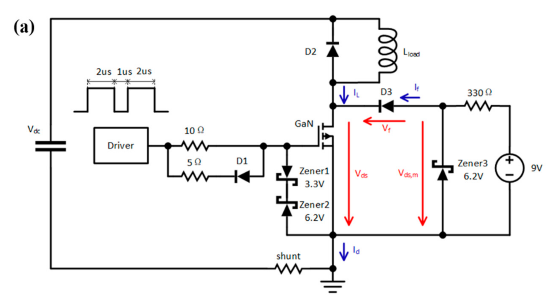
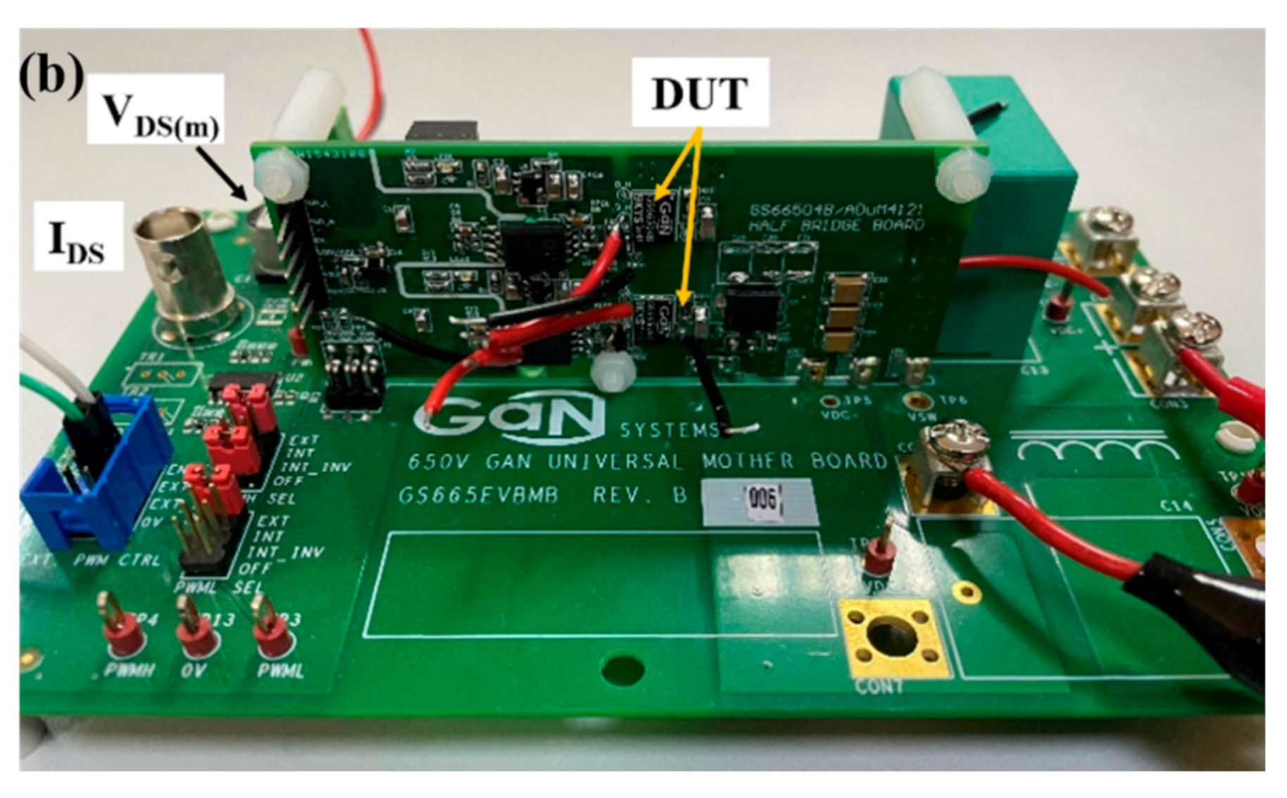
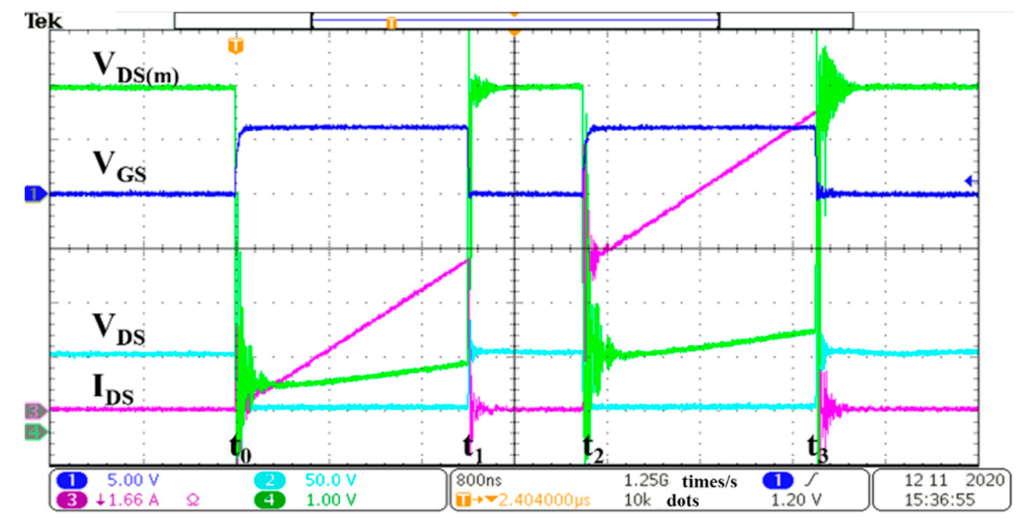
2. Experimental Details
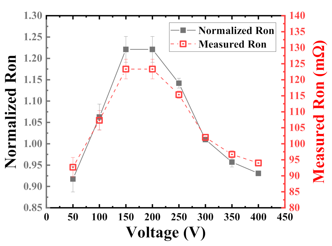
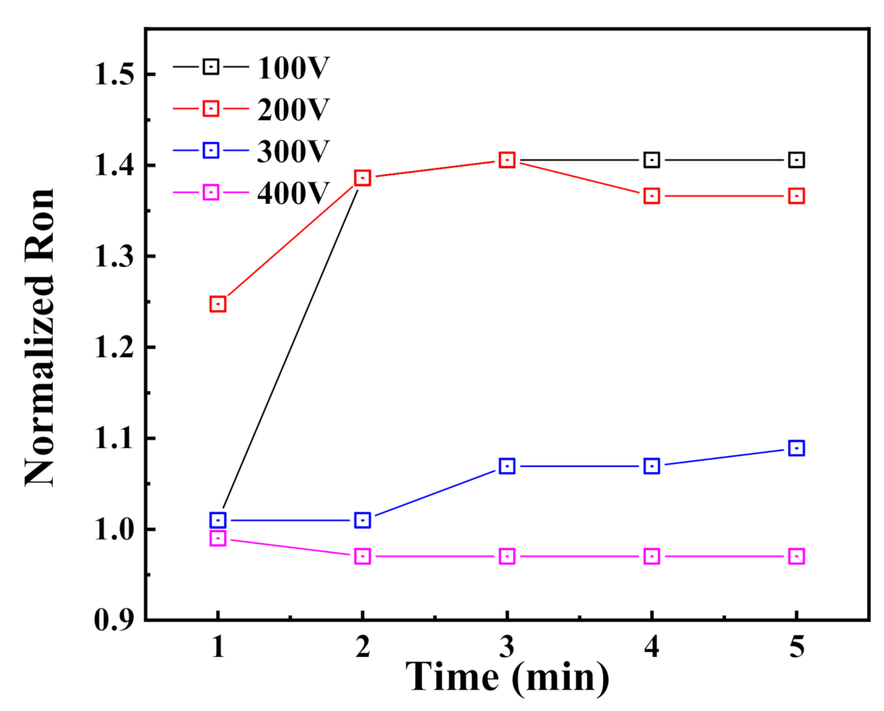
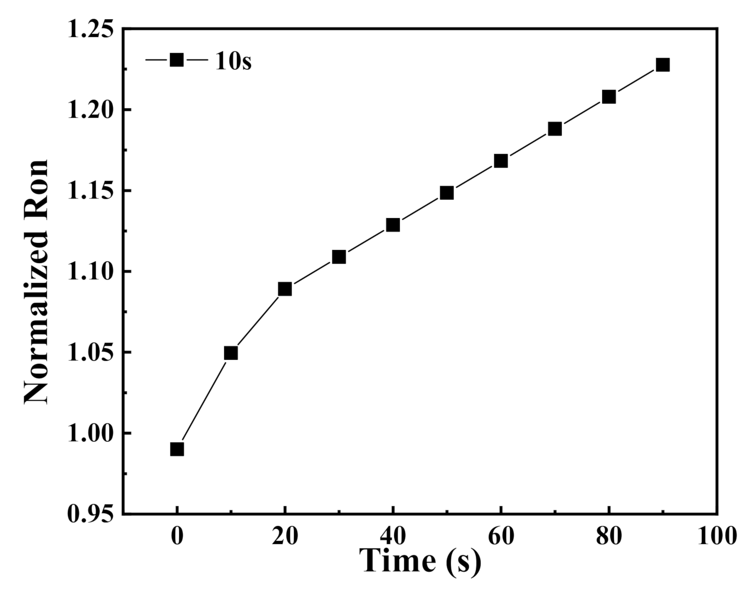
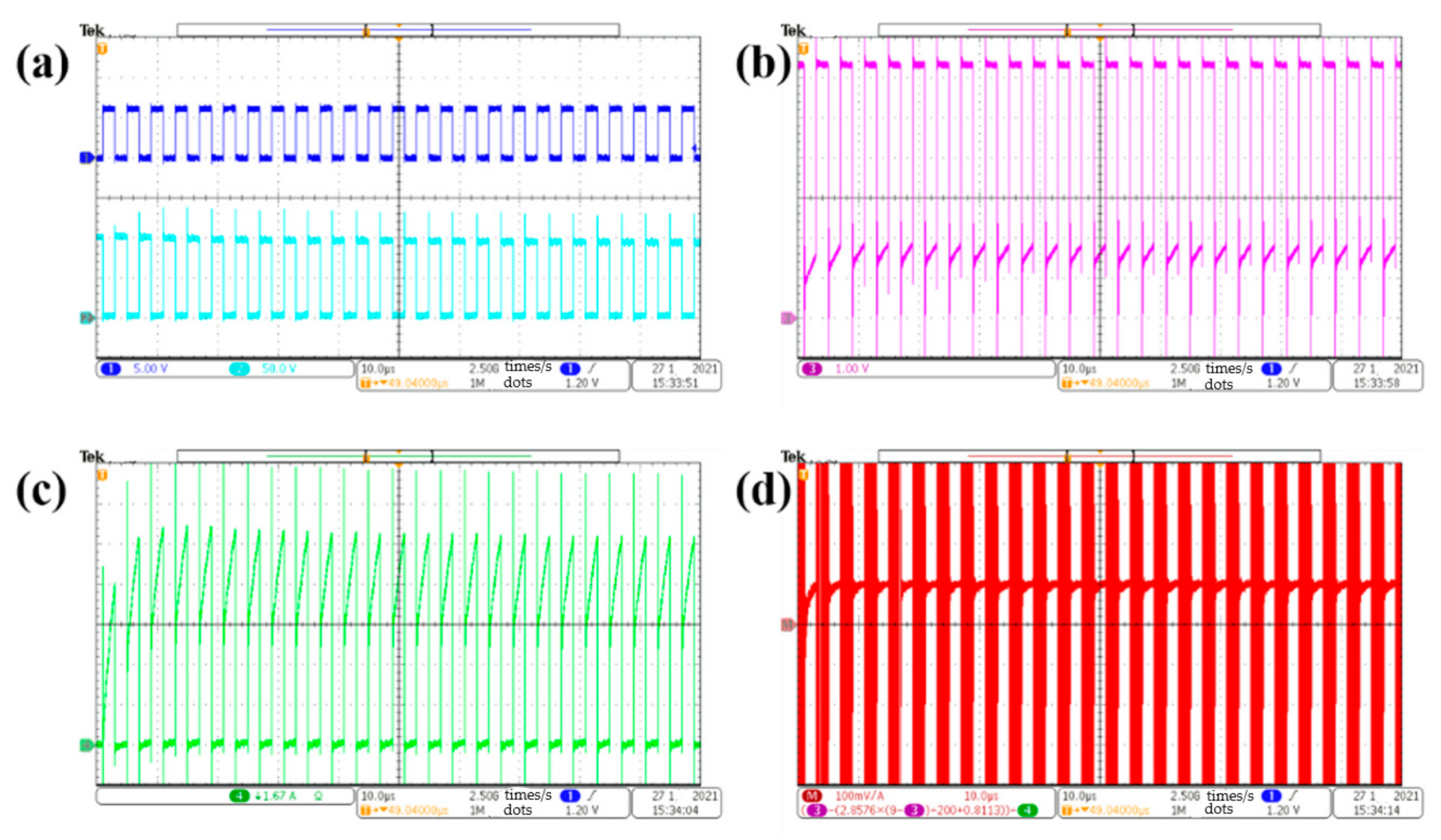
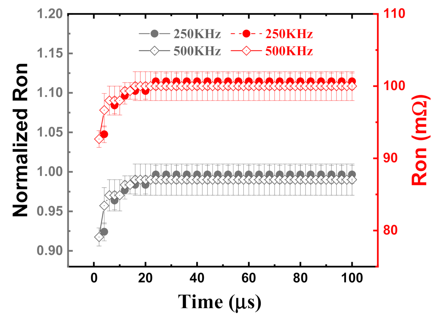
The test circuit schematic used in this paper is shown in Figure 1a, which is widely adopted DPT half-bridge configuration for hard-switching conditions. The control signals are well described previous works [11,17]. The clamping circuit [19] is introduced to avoid saturating the amplifier of the oscilloscope channel, and to ensure accurate results by maintaining the maximum vertical resolution. The method is based on a high voltage, fast-switching zero recovery SiC Schottky diode and a Zener diode. When the DUT is at the off state, which means there is a high voltage supplied (several hundred volts) between source and drain, the diode D3 is also at the off state under a reverse bias. The current flows through low power supply, resistance and a Zener diode. The measured voltage is clamped at the regulation value, which is much lower than the real DUT’s off-state voltage. When the DUT is turned on, the real on-state voltage equals to the measured value subtracting the voltage drop on diode D3. The corresponding homemade test board is depicted in Figure 1b.
The practical testing system includes a DC power supply (HSPY-1000-01), an oscilloscope (Tektronix@MDO3054), an auxiliary power supply (KEITHLEY@2231A-30-3, Keithley Instruments, Solon, OH, USA), a function generator (Tektronix@AFG1022, Tektronix, Beaverton, OR, USA) and a test board.
The actual waveform of the DUT under 50 V off-state voltage is shown in Figure 2. The blue, light blue, purple and green lines indicate the gate voltage (VGS), the drain voltage (VDS), the drain current (IDS) and the clamping voltage (VDS(m)). Before t0, the DUT is under high VDS (ranging from 50 V to 400 V) for a controllable stress time. At t0, the DUT switches to on-state until t1, whose duration is 2 μs. At t1, the current through the DUT increases to 5 A. After an interval of 1 μs, the DUT turns on again for another 2 μs under the second pulse. The device current rises to 10 A at the end of the second pulse. Then, the test finishes at t3 when the DUT is switched off. The dynamic on-state resistance is measured and calculated at 1.96 μs during the second on-state time.

3. Results

Figure 3 displays the dynamic RON variation with different stress voltages ranging from 50 to 400 V; the step is 50 V. The IDS keep the same at 10 A for each voltage, which is adjusted by the external inductor. The detailed value is given in Table 1. At each specific off-state voltage, the dynamic RON is tested three times. Additionally, for the accuracy, the test interval is 20 min to completely release the trapped electrons. The normalized RON is the value of measured dynamic RON values divided by the static on-resistance value extracted from output curves at room temperature.
The device has an evident dynamic RON increase as the voltage initially increases to 150 V, which is consistent with the common understanding of GaN HEMTs [14,15,16,17,19]. Additionally, the dynamic on-resistance degradation is not severe with the highest value of 1.23 at 150 and 200 V. The growing dynamic on-resistance under lower off-state voltage can be explained by the “leaky dielectric” model related with charge storage [20]. The leakage path, which exists between the source and drain contact and the highly resistive carbon-doped GaN layer, allows a hole current to flow from the drain contact into the C-doped layer and forms negatively charged regions at the unintentionally doped (UID)–GaN/C-doped GaN interface as the VDS increases. This negative charge reduces the 2DEG density and leads to the increase in dynamic RON. Another fact for the dynamic on-resistance increases is the hot electron injection, which is due to the overlap of VDS and IDS under hard-switching conditions [4].
However, after experiencing a maximum with the range around 50 V, the dynamic RON starts to decline as the VDC further increases. The descent rate is getting slower and slower. This non-monotonic phenomenon is different from the previous report under the hard-switching conditions [17]. In Reference [17], the authors found similar behavior in a GaN device with a hybrid drain-embedded (HD) structure [21], since the p–n junction in the HD structure endures a voltage drop caused by high channel current when the DUT switches on at a high VDS. It can inject holed into buffer layer to alleviate the current collapse effect by releasing the trapped electrons during the high voltage stress, thus decreasing the dynamic RON. The point is that there is no HD structure in the tested DUT in this paper despite the unknown detailed structure. However, some reasonable explanations can be proposed based on the same point of view (decrease in trapped electrons or increase in holes). The enhanced vertical leakage through the whole area between source and drain [20,22], trapping at donor defects [23], and the two-dimensional hole gas (2DHG) formed at the interface of C-doped GaN and strain relief layer [24] under high VDS will result in a decrease in the number of trapped electrons that cause the reduction in dynamic on-resistance.
For the clarification of the voltage stress superposition effect on the dynamic RON, the time-dependent test is implemented as follows. In Figure 4, normalized RON is plotted versus increasing stressing time under four individual off-state voltages. The DPT is triggered every one minute at a fixed VDS. The curves clearly show that the dynamic Ron degradation is more severe at lower voltage after a period of stress. One of the reasons is the long-time stressing operation which will lead to increased trapping during the off-state and the shorter detrapping time which occurs only during the on-state in each DPT test [4,10]. The accumulated trapping effect is ascribed to both reasons and leads to the increase in dynamic RON. Moreover, a longer trapping time constant associated with deep acceptors and donors as charge reservoirs [20] contributes to the gradual increase in the dynamic on-state resistance in the first 2–3 min.
The resistance increase under 300 V in 5 min is only 8%. At 400 V, the dynamic RON does not even vary with the extended stressing time. A similar phenomenon has been found in the earlier papers [4,25]. They associate this attribution with the field plate normally utilized in the enhancement-mode GaN HEMT devices. This is because the field plate, which is placed between the gate and drain, induces a lateral electric field and inhibits the electron trapping in this area, especially at higher drain and source voltage. Likewise, this suppression is less effective because lateral electric field weakens as the off-state voltage decreases.
Figure 5 shows that the dynamic RON increases with a shorter stress time interval of 10 s when the voltage is fixed at 100 V. It is seen that the dynamic on-state resistance of the DUT displays a gradually increased tendency, indicating that the trapping of electrons is a cumulative process. The phenomenon of this gradual increase can be explained as the response to the donor/acceptor in the UID and/or C-doped GaN layer caused by not only the intrinsic trap time constant but also the charge transport in the buffer stack [20], which takes longer time.
In order to simulate the real working situation of the GaN HEMT device in a converter, the continuous operation was carried out to evaluate the dynamic on-resistance under two frequencies of 250 and 500 kHz. The actual waveform of 250 kHz under 100 V off-state voltage is shown in Figure 6. The heat dissipation, ascribed to conduction loss, can be estimated by the by P = IR2. The current and dynamic on-resistance are 10 V and 100 mΩ, respectively. Take the duty cycle of 0.5 into account, the heat dissipation power is less than 5 W. So, the maximum temperature increase is 5 ℃ to the bottom side. Additionally, the total evaluation time is limited to 100 μs to avoid self-heating.
The measured dynamic RON is plotted in Figure 7 with the total continuous operation time. The multi-pulse test is implemented only for 100 V off-state voltage since the dynamic on-resistance performs a more severe increase. For both frequencies, the resistance increases in the first 10 μs and then gets to a nearly steady value with the increase in pulse number. The results of multi-pulse measurement are consistent with that of DPT [17]. Additionally, there is no difference in the steady value between 250 and 500 kHz, which means that the frequency does not affect the dynamic RON. It indicates that the trapping during the high-power switching and detrapping during the on-state reach an equilibrium in a very short time for a high-frequency switching operation. It can be interpreted by the deep level trap with a longer time constant. Unlike the test in Figure 4, the off-state time is 2 μs in each pulse, meaning the electrons do not have enough time to respond to the high frequency.
It is well acknowledged that dynamic RON is more sensitive to frequency under hard-switching conditions attributed to hot electrons [26]. However, based on the results above, it is assumed that a leaky dielectric mechanism should contribute more to the increase in dynamic on-resistance in a voltage stress experiment, as discussed in Figure 3.

4. Conclusions

In this paper, we investigated the dynamic on-resistance behavior of one commercial GaN HEMT device with p-GaN gate under hard-switching conditions. The dynamic RON shows a non-monotonic performance, which initially increases to 1.22 times the static value and then decreases with the increasing off-state voltage. The stress time dependence of dynamic RON with various VDS displays different characteristics. Only under lower VDS does dynamic RON increase gradually and reach a saturated level. The electron trapping effect was weakened when the field plate was applied as the common technology in GaN HEMT, resulting in no obvious rise of RON. The multi-pulse test, matched to the practical application, implies little frequency correlation and dynamic resistance degradation. All the results suggest that the leakage in the dielectric plays an important role in the dynamic performance. More quantitative investigations should be implemented to fully understand the dynamic characteristics of GaN HEMT.

Author Contributions

Conceptualization, W.W. and Y.L.; methodology, Y.L.; software, M.Z.; validation, W.W., M.Z. and Y.L.; formal analysis, Y.L.; investigation, F.L.; resources, M.Z.; data curation, F.L.; writing—original draft preparation, W.W.; writing—review and editing, F.L. and F.W.; visualization, F.L.; supervision, H.W.; project administration, W.W. and H.W.; funding acquisition, W.W. and H.W. All authors have read and agreed to the published version of the manuscript.

Funding

This research was funded by National Key Research and Development Program (No. 2017YFB0402802, 2018YFE0125900), the National Natural Science Foundation of China (Nos. 61804122, 61627812), Shaanxi Key Research and Development Program (No. 2021GY-223) and China Postdoctoral Science Foundation (2019M660256).

Data Availability Statement

Experimental data is available upon request.

Conflicts of Interest

The authors declare no conflict of interest.

References

  1. Moens, P.; Banerjee, A.; Coppens, P.; Declercq, F.; Tack, M. AlGaN/GaN power device technology for high current (100+A) and high voltage (1.2 kV). In Proceedings of the 2016 28th International Symposium on Power Semiconductor Devices and ICs (ISPSD), Prague, Czech Republic, 12–16 June 2016; pp. 455–458. [Google Scholar] [CrossRef]
  2. Vetury, R.; Zhang, N.Q.; Keller, S.; Mishra, U.K. The impact of surface states on the DC and RF characteristics of AlGaN/GaN HFETs. IEEE Trans. Electron. Devices 2001, 48, 560–566. [Google Scholar] [CrossRef]
  3. Meneghini, M.; Zanoni, E.; Meneghesso, G. Gallium nitride based HEMTs for power applications: High field trapping issues. In Proceedings of the 2014 12th IEEE International Conference on Solid-State and Integrated Circuit Technology (ICSICT), Guilin, China, 28–31 October 2014; pp. 1–4. [Google Scholar] [CrossRef]
  4. Hwang, I.; Kim, J.; Chong, S.; Choi, H.-S.; Hwang, S.-K.; Oh, J.; Shin, J.K.; Chung, U. Impact of Channel Hot Electrons on Current Collapse in AlGaN/GaN HEMTs. IEEE Electron. Device Lett. 2013, 34, 1494–1496. [Google Scholar] [CrossRef]
  5. Rossetto, I.; Meneghini, M.; Tajalli, A.; Dalcanale, S.; De Santi, C.; Moens, P.; Banerjee, A.; Zanoni, E.; Meneghesso, G. Evidence of Hot-Electron Effects During Hard Switching of AlGaN/GaN HEMTs. IEEE Trans. Electron. Devices 2017, 64, 3734–3739. [Google Scholar] [CrossRef]
  6. Jones, E.A.; Wang, F.F.; Costinett, D. Review of Commercial GaN Power Devices and GaN-Based Converter Design Challenges. IEEE J. Emerg. Sel. Top. Power Electron. 2016, 4, 707–719. [Google Scholar] [CrossRef]
  7. Hilt, O.; Bahat-Treidel, E.; Cho, E.; Singwald, S.; Wurfl, J. Impact of buffer composition on the dynamic on-state resistance of high-voltage AlGaN/GaN HFETs. In Proceedings of the 2012 24th International Symposium on Power Semiconductor Devices and ICs, Bruges, Belgium, 3–7 June 2012; pp. 345–348. [Google Scholar] [CrossRef]
  8. Zhang, W.; Xu, Z.; Zhang, Z.; Wang, F.; Tolbert, L.M.; Blalock, B.J. Evaluation of 600 V cascode GaN HEMT in device characterization and all-GaN-based LLC resonant converter. In Proceedings of the 2013 IEEE Energy Conversion Congress and Exposition, Denver, CO, USA, 15–19 September 2013; pp. 15–19. [Google Scholar] [CrossRef]
  9. Josifovic, I.; Popovic-Gerber, J.; Ferreira, J.A. Improving SiC JFET Switching Behavior under Influence of Circuit Parasitics. IEEE Trans. Power Electron. 2012, 27, 3843–3854. [Google Scholar] [CrossRef]
  10. Badawi, N.; Hilt, O.; Bahat-Treidel, E.; Bocker, J.; Wurfl, J.; Dieckerhoff, S. Investigation of the Dynamic On-State Resistance of 600 V Normally-Off and Normally-On GaN HEMTs. IEEE Trans. Ind. Appl. 2016, 52, 4955–4964. [Google Scholar] [CrossRef]
  11. Cai, Y.; Forsyth, A.J.; Todd, R. Impact of GaN HEMT dynamic on-state resistance on converter performance. IEEE Appl. Power Electron. Conf. Expo. (APEC) 2017, 1689–1694. [Google Scholar] [CrossRef]
  12. Jones, E.A.; Pozo, A. Hard-Switching Dynamic Rds,on Characterization of a GaN FET with an Active GaN-Based Clamping Circuit. In Proceedings of the 2019 IEEE Applied Power Electronics Conference and Exposition (APEC), Anaheim, CA, USA, 17–21 March 2019; pp. 2757–2763. [Google Scholar] [CrossRef]
  13. Burgos, R.; Zheng, C.; Boroyevich, D.; Wang, F. Design considerations of a fast 0-Ω gate-drive circuit for 1.2 kV SiC JFET devices in phase-leg configuration. In Proceedings of the 2009 IEEE Energy Conversion Congress and Exposition, San Jose, CA, USA, 20–24 September 2009; pp. 2293–2300. [Google Scholar] [CrossRef]
  14. Yao, T.; Ayyanar, R. A Multifunctional Double Pulse Tester for Cascode GaN Devices. IEEE Trans. Ind. Electron. 2017, 64, 9023–9031. [Google Scholar] [CrossRef]
  15. Wang, H.; Wei, J.; Xie, R.; Liu, C.; Tang, G.; Chen, K.J. Maximizing the Performance of 650-V p-GaN Gate HEMTs: Dynamic RON Characterization and Circuit Design Considerations. IEEE Trans. Power Electron. 2017, 32, 5539–5549. [Google Scholar] [CrossRef]
  16. Lu, B.; Palacios, T.; Risbud, D.; Bahl, S.; Anderson, D.I. Extraction of Dynamic On-Resistance in GaN Transistors: Under Soft- and Hard-Switching Conditions. In Proceedings of the 2011 IEEE Compound Semiconductor Integrated Circuit Symposium (CSICS), Waikoloa, HI, USA, 16–19 October 2011; pp. 1–4. [Google Scholar] [CrossRef]
  17. Li, R.; Wu, X.; Yang, S.; Sheng, K. Dynamic On-state Resistance Test and Evaluation of GaN Power Devices under Hard and Soft Switching Conditions by Double and Multiple Pulses. IEEE Trans. Power Electron. 2019, 34, 1044–1053. [Google Scholar] [CrossRef]
  18. GS66504B-650V Enhancement Mode GaN Transistor. Available online: https://gansystems.com/gan-transistors/gs66504b/ (accessed on 13 May 2021).
  19. Badawi, N.; Dieckerhoff, S. A new method for dynamic Ron extraction of GaN power HEMTs. In Proceedings of the PCIM Europe 2015; International Exhibition and Conference for Power Electronics, Intelligent Motion, Renewable Energy and Energy Management (PCIM), Nuremberg, Germany, 19–21 May 2015; pp. 1–6. [Google Scholar]
  20. Uren, M.J.; Karboyan, S.; Chatterjee, I.; Pooth, A.; Moens, P.; Banerjee, A.; Kuball, M. “Leaky Dielectric” Model for the Suppression of Dynamic RON in Carbon-Doped AlGaN/GaN HEMTs. IEEE Trans. Electron. Devices 2017, 64, 2826–2834. [Google Scholar] [CrossRef] [Green Version]
  21. Kaneko, S.; Kuroda, M.; Yanagihara, M.; Ikoshi, A.; Okita, H.; Morita, T.; Takana, K.; Hikita, M.; Uemoto, Y.; Takahashi, S.; et al. Current-collapse-free operations up to 850 V by GaN-GIT utilizing hole injection from drain. In Proceedings of the 2015 IEEE 27th International Symposium on Power Semiconductor Devices & IC’s (ISPSD), Hong Kong, China, 10–14 May 2015; pp. 41–44. [Google Scholar] [CrossRef]
  22. Cornigli, D.; Reggiani, S.; Gnani, E.; Gnudi, A.; Baccarani, G.; Moens, P.; Vanmeerbeek, P.; Banerjee, A.; Meneghesso, G. Numerical investigation of the lateral and vertical leakage currents and breakdown regimes in GaN-on-Silicon vertical structures. In Proceedings of the 2015 IEEE International Electron Devices Meeting (IEDM), Washington, DC, USA, 7–9 December 2015; pp. 109–112. [Google Scholar] [CrossRef]
  23. Zhou, C.; Jiang, Q.; Huang, S.; Chen, K.J. Vertical Leakage/Breakdown Mechanisms in AlGaN/GaN-on-Si Devices. IEEE Electron. Device Lett. 2012, 33, 1132–1134. [Google Scholar] [CrossRef]
  24. Chatterjee, I.; Uren, M.J.; Karboyan, S.; Pooth, A.; Moens, P.; Banerjee, A.; Kuball, M. Lateral Charge Transport in the Carbon-Doped Buffer in AlGaN/GaN-on-Si HEMTs. IEEE Trans. Electron. Devices 2017, 64, 977–983. [Google Scholar] [CrossRef] [Green Version]
  25. Moens, P.; Liu, C.; Banerjee, A.; Vanmeerbeek, P.; Coppens, P.; Ziad, H.; Constant, A.; Li, Z.; Vleeschouwer, H.D.; RoigGuitart, J.; et al. An industrial process for 650V rated GaN-on-Si power devices using in-situ SiN as a gate dielectric. In Proceedings of the 2014 IEEE 26th International Symposium on Power Semiconductor Devices & IC’s (ISPSD), Waikoloa, HI, USA, 15–19 June 2014; pp. 374–377. [Google Scholar] [CrossRef]
  26. Meneghini, M.; Stocco, A.; Silvestri, R.; Ronchi, N.; Meneghesso, G.; Zanoni, E. Impact of hot electrons on the reliability of AlGaN/GaN High Electron Mobility Transistors. In Proceedings of the 2012 IEEE International Reliability Physics Symposium (IRPS), Anaheim, CA, USA, 15–19 April 2012; pp. 2C.2.1–2C.2.5. [Google Scholar] [CrossRef]
Figure 1. (a) Gallium nitride-high electron mobility transistor (GaN-HEMT) dynamic on-state resistance test circuit for hard-switching conditions with clamping circuit; (b) actual test board.
Electronics 10 01202 g001aElectronics 10 01202 g001b
Figure 2. The real waveform of tested gate voltage (VGS, blue line), drain and source voltage (VDS, cyan line), measured VDS (green line), and drain current (IDS, purple line).
Electronics 10 01202 g002
Figure 3. Normalized and measured dynamic on-resistance (RON) value at 1.96 μs after turn on for different voltage stresses by the double pulse test (DPT) method.
Electronics 10 01202 g003
Figure 4. Normalized RON value for increasing stress times with the interval of 60 s at off-state voltage from 100 to 400 V.
Electronics 10 01202 g004
Figure 5. Normalized RON value for increasing stress times with shorter intervals at 100 V off-state voltage.
Electronics 10 01202 g005
Figure 6. The real waveform of a multi-pulse test at 100 V and 250 kHz: (a) VGS and VDS; (b) VDS(m); (c) IDS; (d) dynamic RON.
Electronics 10 01202 g006
Figure 7. Normalized and measured dynamic RON value at 1.96 μs in every pulse under 250 kHz and 500 kHz.
Electronics 10 01202 g007
Table 1. Inductors corresponding to the different off-state voltages.
VDC (V)50100150200250300400
Inductor (μH)20406080100120160
Publisher’s Note: MDPI stays neutral with regard to jurisdictional claims in published maps and institutional affiliations.

