1. Introduction
The traditional processor uses the von Neumann structure, in which the storage unit and the processing unit are separated and connected by bus. In recent years, with the development of semiconductor technology, the speed of processing units has been greatly improved. However, due to the limitation of bus bandwidth, the operation speed of the whole processor is limited, which is called the “von Neumann bottleneck problem” [
1,
2]. In order to solve this problem, inspired by the biological way of processing information, many pieces of literature have proposed various non-von Neumann processor solutions [
3,
4,
5]. Typical bio-inspired computing relies on nonlinear networks that contain the same cells; each cell has a relatively simple structure and interacts with the surrounding cells. This structure, called a CNN, a cellular neural network, has been applied in fields such as computer vision [
6,
7,
8].
The concept of a CNN can be traced back to two articles by Chua in 1988 [
9,
10], which respectively give the theory and application of CNNs. Recently, Itoh [
11] summarized some characteristics of CNNs in a long paper. Weiher et al. [
12] discussed the pattern formation of CNNs based on the NbO
2 memristor.
Recently, brain-like computing has become a hot topic in research [
13,
14,
15], and the key is to find devices that can produce spike signals like neurons and that have very low power consumption. The VO
2 carbon nanotube (CNT) composite device is a Mott memristor recently proposed [
16]. It can generate periodic peak pulses with a pulse width of less than 20 ns, it is driven by a DC current or voltage, and it does not need additional capacitance. It uses metal–carbon nanotubes as heaters, and, compared with the pure Mott VO
2 proposed earlier, adding CNTs can greatly reduce the transient duration and pulse energy and increase the frequency of a peak pulse by three orders of magnitude.
The VO
2 nano crossbar device does not need the process of electric forming and has low device size dispersion. For devices with a critical size between 50 and 600 nm, the change coefficient of the switch threshold voltage is less than 13%, the switch durability is more than 26.6 million cycles, and the IV characteristics of the device are not changed significantly. The VO
2 device technology in the process of non-electric formation accelerates the development of an active memristor neuron circuit. It can simulate the most known neuron dynamics and clear the way for the realization of a large-scale integrated circuit (IC). In addition, the VO
2 memristor is superior to its NbO
2 counterpart in both switch speed and switching energy. The simulated Mott transition in the VO
2 is 100 times faster than in the NbO
2 and consumes only about one-sixth (16%) of the energy [
17].
In this paper, a cellular neural network based on a VO2 CNT is proposed. As a cell itself, a VO2 CNT is set to be stable and static, that is, in “sleep”. If the memristor is on the “edge of chaos”, two or more cells are connected by the RC coupling, which will make it in the state of “wake-up”, namely, in the dynamic oscillation mode. The second part of this paper is the modeling of VO2 CNT composite devices, providing the SPICE model. The third part is the cell circuit, which gives the analysis process of the decoupled circuit. The response of the memristor is expanded near the operating point and the small-signal equivalent circuit is given. Based on this, the influence of coupling R and C device parameters on the input impedance of one port is analyzed. The fourth part is the CNN simulation, which describes the pattern formation characteristics of a CNN composed of memristor-based cells.
Compared with the traditional CMOS realization of CNN, the memristor counterpart can largely save power and chip area, and provide ultra-high processing speeds.
2. VO2 Carbon Nanotube Composite Device Modeling
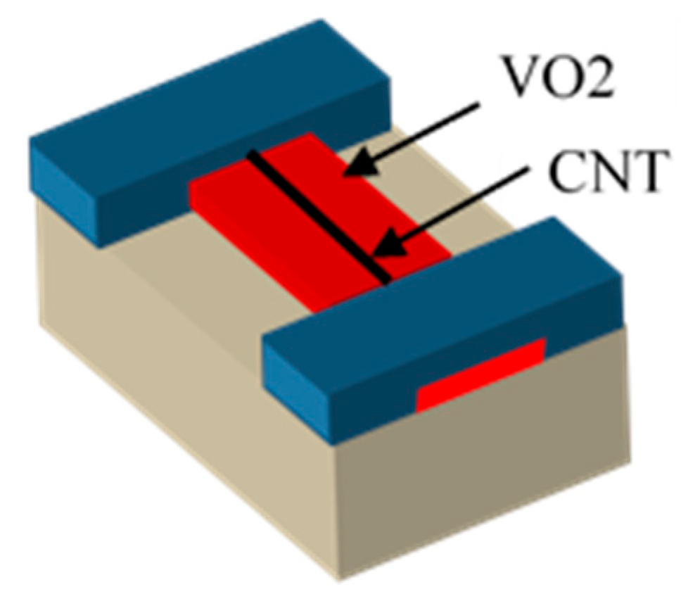
The structure of the VO
2 carbon nanotube composite device is shown in
Figure 1. It contains a transverse active region, which is defined by a VO
2 thin metal strip with a thickness of about 5 nm (as shown in the red region of the figure), and its two ends are connected with Pd electrodes (as shown in the blue region of the figure). This is a planar Mott metal-insulator transition device. The aligned carbon nanotubes (as shown in the black line) were first grown on quartz substrate, and then transferred to the surface of a VO
2 thin metal strip before the whole device was formed.
As a Mott metal-insulator transition device, it satisfies the following equation [
16]:
The first formula of Equation (1) is the current emission equation of the Schottky diode, and the second formula is Newton’s cooling law, where,
im and 𝑣
m are the current and voltage through the memristor NDR device, respectively;
T is the absolute temperature of the device;
Tamb is the ambient temperature;
A and 𝛽 are scaling constants;
d is the effective device length;
k is Boltzmann constant;
is the energy barrier;
Cth is the heat capacity (effective thermal mass);
Rth is the thermal resistance;
RCNT is the resistance value of the CNT (carbon nanotube), taking 600 kΩ. The second expression of Equation (1) represents the electrical and thermal coupling between
RCNT and VO
2. The parameters of the device are shown in
Table 1.
According to Equation (1), the SPICE model of the device can be established, as shown in
Figure 2The quasi-static volt-ampere characteristics of the device can be obtained by using the SPICE model, as shown in
Figure 3.
The simulation measurement method of the quasi-static volt-ampere characteristics of the device is to use a sinusoidal voltage source with a frequency of 1 Hz and amplitude of 10 V to excite the device through a small series resistor, and then draw the V–I relationship curve by measuring the current flowing through the device. When you look at
Figure 3, you can clearly see a hysteresis region, which is a typical feature of the local active memristor.
3. Cell Circuit
Figure 4 is the designed circuit of a memristor cell, in which
is the bias resistor, M is the VO
2 memristor and
is the carbon nanotube resistance. The parallel resistor and capacitor combination is the circuit coupled with adjacent cells, and it is also a part of the cell.
According to
Figure 4, the circuit equation can be obtained by using the Kirchhoff current law, the Kirchhoff voltage law and Equation (1), as follows:
In order to make it easy to write a MATLAB simulation program, Equations (2) and (3) can be further arranged into a matrix form, as follows:
where
The necessary conditions for the local activity of resistive-coupled reaction–diffusion CNNs (RD-CNNs) are given in [
18]. In order to apply the theory to the designed network, the input impedance Z of port A must be calculated. Therefore, it is necessary to linearize Equation (4) near the operating point without coupling, that is to say, the small-signal equivalent circuit analysis condition is satisfied under the condition of a zero-port current. The memristor equation is expanded near the operating point.
Here, , and are the state, voltage and current values of the DC operating point, respectively.
We can expand the expression of the memristor current near the operating point:
where
h.o.t. is the higher-order term relative to
and
. If
and
, we can get the following approximate linear relationship:
Next, we will expand the memristor equation of state with a Taylor series near the operating point
:
where
Notice that
, because
is a point on the DC V–I curve. Ignoring the high-order small term, let us linearize the memristor state Equation (13) near the operating point:
Taking Laplace transform for Equations (12) and (15), we obtain
The Laplace transforms of
,
and
are
,
and
. According to the second formula of (16), we obtain:
According to the first formula of (16) and Equation (17), the admittance function of the memristor can be obtained as follows:
Change Equation (18) into the following form:
is the admittance of the memristor. The small signal equivalent circuit of the memristor is shown in
Figure 5.
,
and
are defined as follows:
Considering the DC bias of the cell circuit, according to Equation (2), and that the R and C parameter values do not affect the DC operating point of the system, let , , respectively. Then, we use MATLAB to solve the DC operating point Q, , and substitute the operating point value into Equation (20), we can evaluate , and respectively.
The equivalent impedance of port A in the frequency domain is obtained.
In [
18], Professor Chua derived the local active condition of resistive coupled RD-CNNs based on the reaction–diffusion equation. It is said that the cell is in the local active region if the input impedance of the one port cell satisfies at least one of the following conditions:
- (a)
There is a pole in the right half plane;
- (b)
There are higher-order poles on the imaginary axis;
- (c)
There is a pole of order one on the imaginary axis and is a negative real number or a complex number with non-zero imaginary part;
- (d)
There is at least one angular frequency value , such that the real part of the impedance is less than zero.
Through calculation, the system impedance
has the following form:
where
A is the real coefficient. According to Chua’s theory [
18], the system described by conditions (a)–(c) is unstable, while the system is a stable local active system when condition (d) is satisfied along with the poles being in the left half plane, that is, the system is located in the edge of chaos. In addition, according to the theory of signals and systems,
is the transfer function of the system. When the poles of
, corresponding to the zeroes, is located in the right half plane of the complex plane, the system will be unstable, and the system is said to be on the sharp edge of chaos. Specifically, because the numerator of the input impedance is a quadratic polynomial, its zeroes correspond to two cases: the system has two positive zeroes (two zeroes whose real part is greater than zero; they are conjugate zeroes, i.e.,
z1 ≠
z2,
Re(
z1) > 0 and
Re(
z2) > 0) or one positive real zero (zero is a positive real number as multiple roots, (
z1 =
z2) > 0), corresponding to dynamic pattern and static pattern, respectively.
In
Figure 6, yellow indicates that the system is in the local passive area and the input impedance does not meet Condition (d); the other areas are in the local active area and the input impedance meets Condition (d). Blue indicates that the system is at the sharp edge of chaos. At this time, the impedance function of the system has two positive zeroes (two zeroes whose real parts are greater than zero; they are conjugate zeroes) or one positive real zero (zero is a positive real number as multiple roots), which correspond to the dark blue and light blue regions, respectively. Other regions in the figure, that is, when green corresponds to other cases of zeroes, indicate that the system is at the edge of chaos. In
Figure 6, the edge region of chaos, that is, the light green Region II, contains coupling parameters that may not destabilize the system because the resulting local input impedance of the cell does not have the zero point of the positive real part. On the other hand, the union of the dark blue Region III and the light blue Region IV represents the sharp edge of chaos. In the dark blue Region III, the local input impedance of the cell allows a pair of complex conjugate zeroes with positive real parts, which makes the system unstable and leads to the formation of a dynamic pattern in a steady state. In the light blue Region IV, a zero point of the local input impedance of a single cell is positive and real, which triggers the instability of the system and gradually leads to a static mode. It has been proved by literature [
12] that when the cell is in the sleeping mode, the "cell" equation has only a steady-state homogeneous solution; only when the cell is in the sharp edge of chaos can it be successfully “awakened” when it is connected to the CNN; that is to say, the system equation has a non-homogeneous solution, and the light blue region is in so-called “static wake-up”. When a cell is connected to a network, it has a non-homogeneous static stable solution, which is different from when the cell is isolated; the dark blue region is called a dynamic wake-up, which causes oscillation when the cell is connected to the network, so it has a dynamic oscillation solution, which is different from the static solution when the cell is isolated. Because the capacitance value of static wake-up is too large, it is not practical for an integrated system. Only a dynamic wake-up is considered.
4. CNN and Simulation
Connect two cells, and the common resistance and capacitance can be equivalent to two identical series connections [
12] by the circuit principle, so as to distribute them to each cell, as shown in
Figure 7.
Select
R = 1 MΩ,
C = 720 p, corresponding to
,
; the two cells are in sleeping mode before coupling, as shown in
Figure 8. In
Figure 8b, the voltage decreases from 10 V to 0 V, and the cell does not oscillate.
After coupling, it is in wake-up mode, as shown in
Figure 9.
Figure 9b shows that the voltage drops from the initial 10 V to oscillate near 0 V.
It can be seen from
Figure 8 and
Figure 9 that when the cell is in the sleeping mode, both cells do not oscillate, and the differential equation of the system has only a trivial solution, that is, a zero solution. When the cell is in wake-up mode, the differential equation of the cell system has oscillatory solutions, and different cells get different oscillatory solutions.
In order to observe the characteristics of a CNN composed of cells, 5 × 5 cells are arrayed, as shown in
Figure 10, and the DC excitation of each cell rises to 10 V in 1 u seconds. The cells in the central position (3,3) are deliberately raised to 10 V in 0.9 u seconds. The voltage response of 25 cells is observed, as shown in
Figure 11.
It can be seen from
Figure 11 that after a short transient response, each cell reaches steady-state oscillation. According to
Figure 11, the network pattern diagram at different times can be made, as shown in
Figure 12, in which different colors represent different terminal voltages of the cellular memristor.
Figure 12 is just a reproduction of
Figure 11 from another view of the spatial distribution of the sampled voltage at a specific time, where, in the vertical axis, “1” represents the highest voltage of the cell, and other values are just the normalized voltage relating to that cell respectively. This is called the pattern of the network. From the figure, it can be seen that the initial conditions can affect the network pattern formation, so that the power source voltage of each cell can be programmed to obtain a specific pattern, so as to complete the information processing.


