
An Experimental Comparison of Galvanically Isolated DC-DC Converters: Isolation Technology and Integration Approach


Abstract
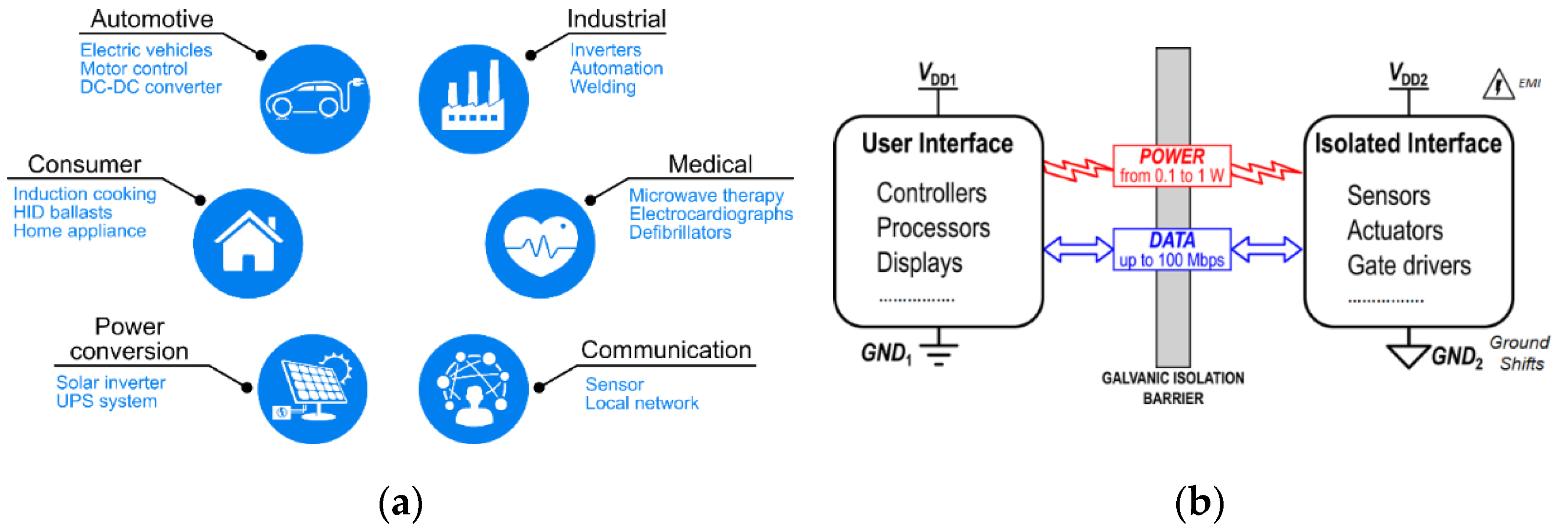
:1. Introduction
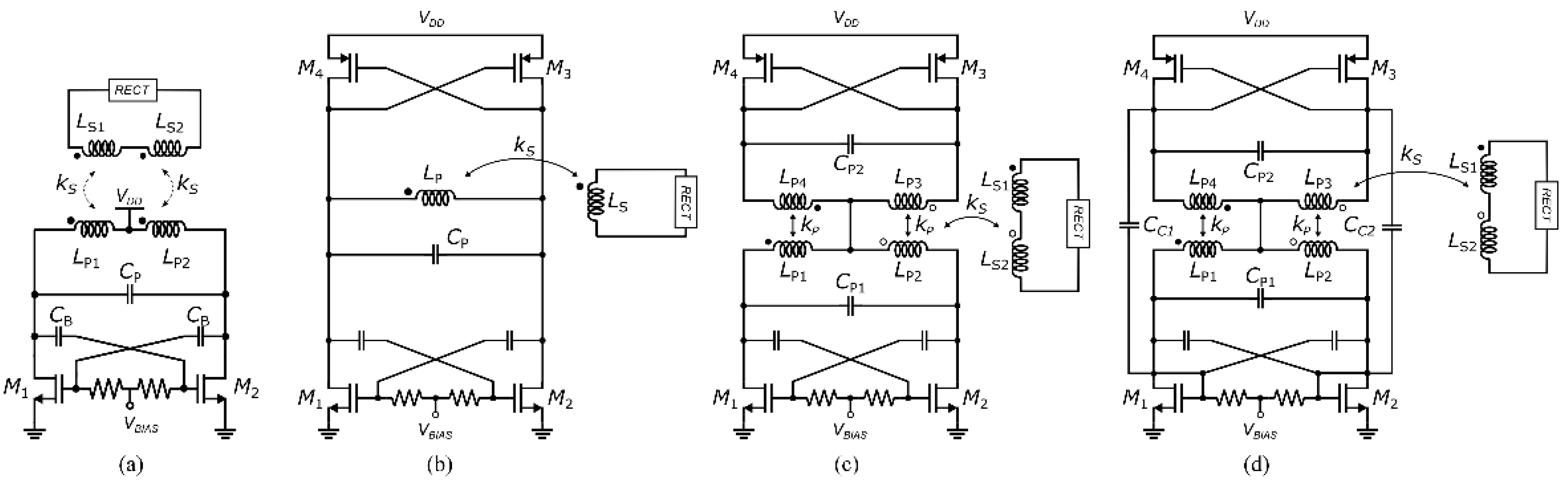
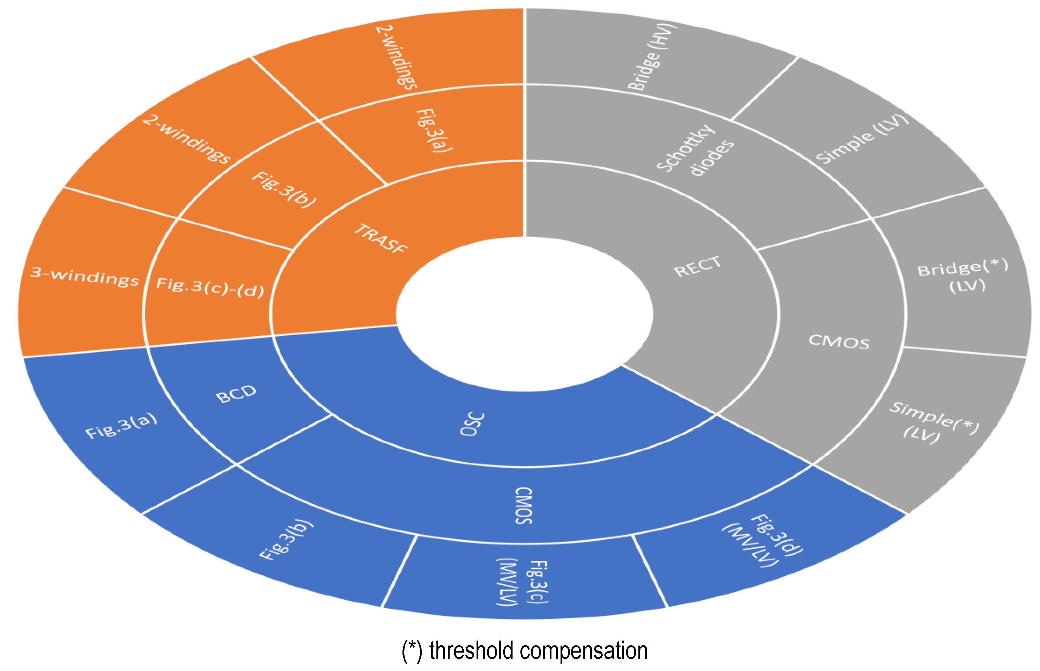
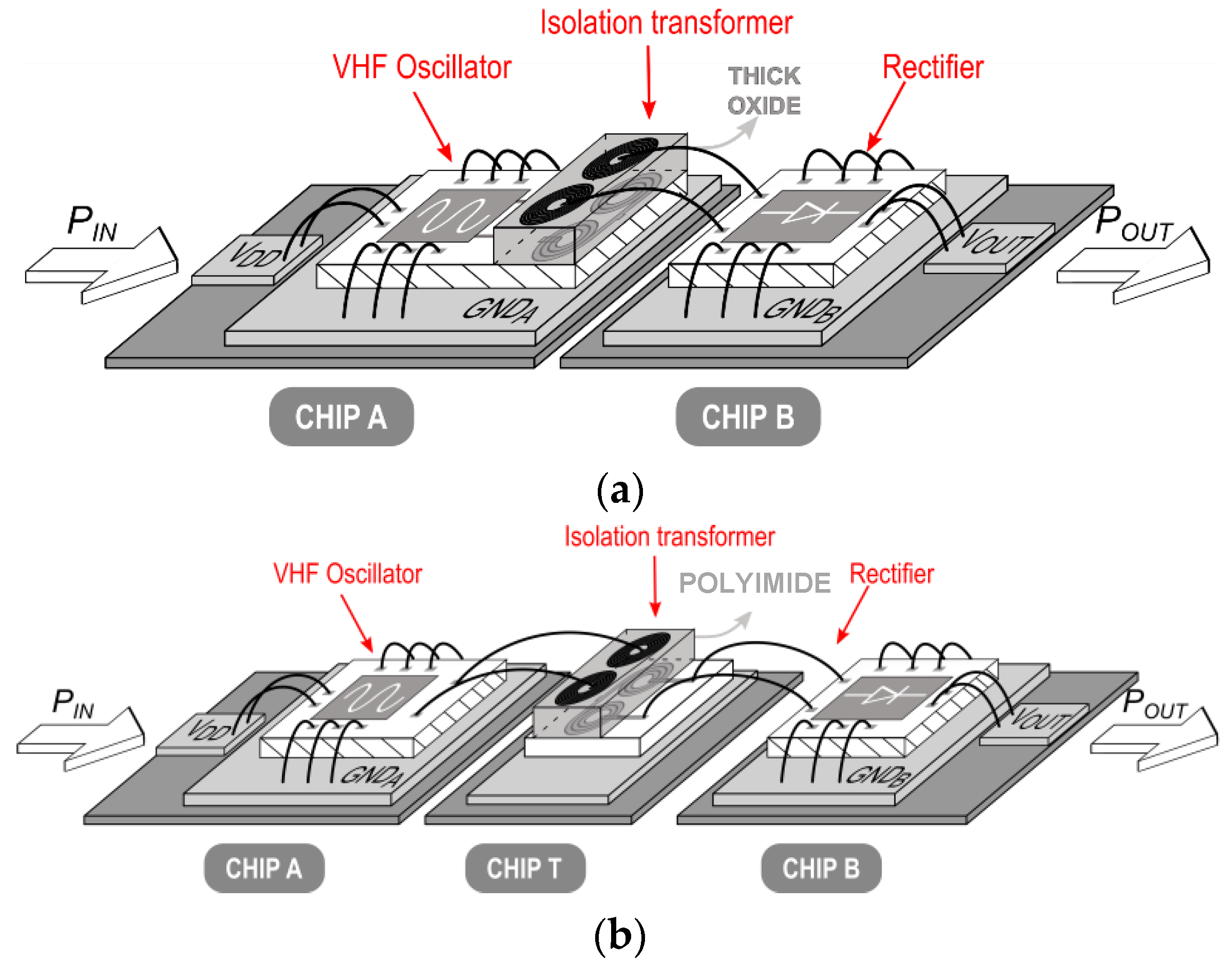
2. Galvanically Isolated DC-DC Conversion: System and Circuit Description
3. Isolation Technology
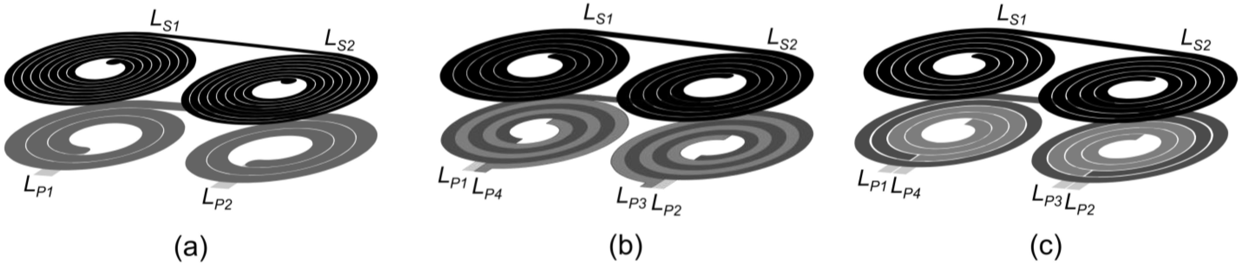
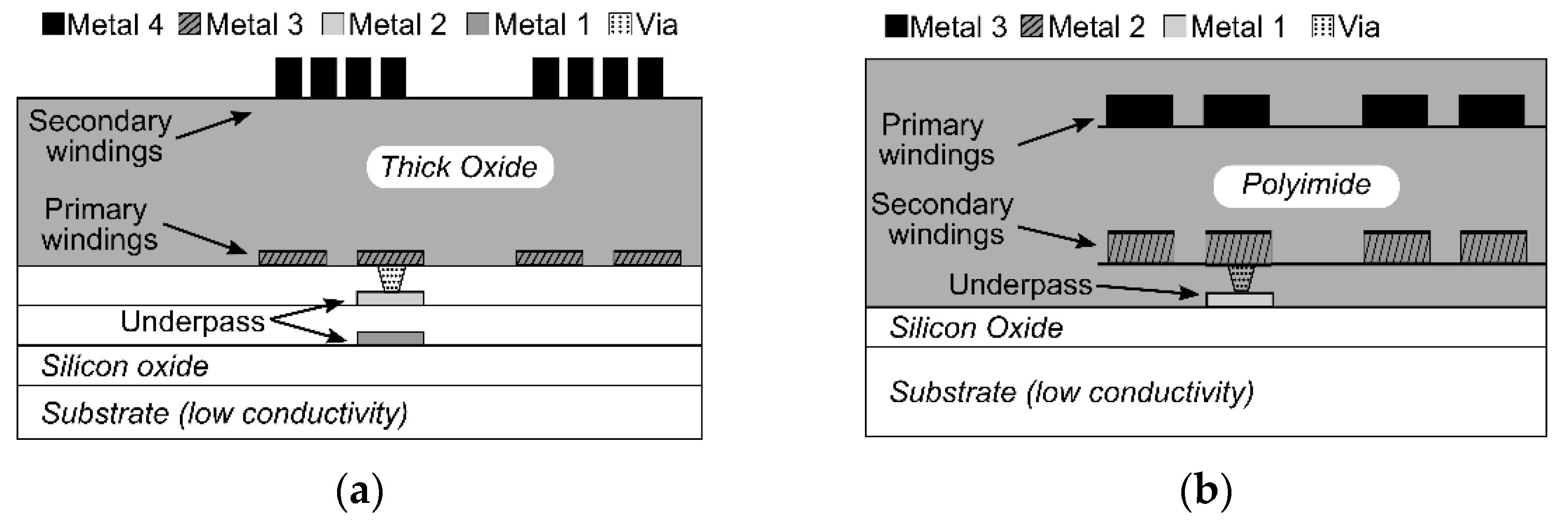
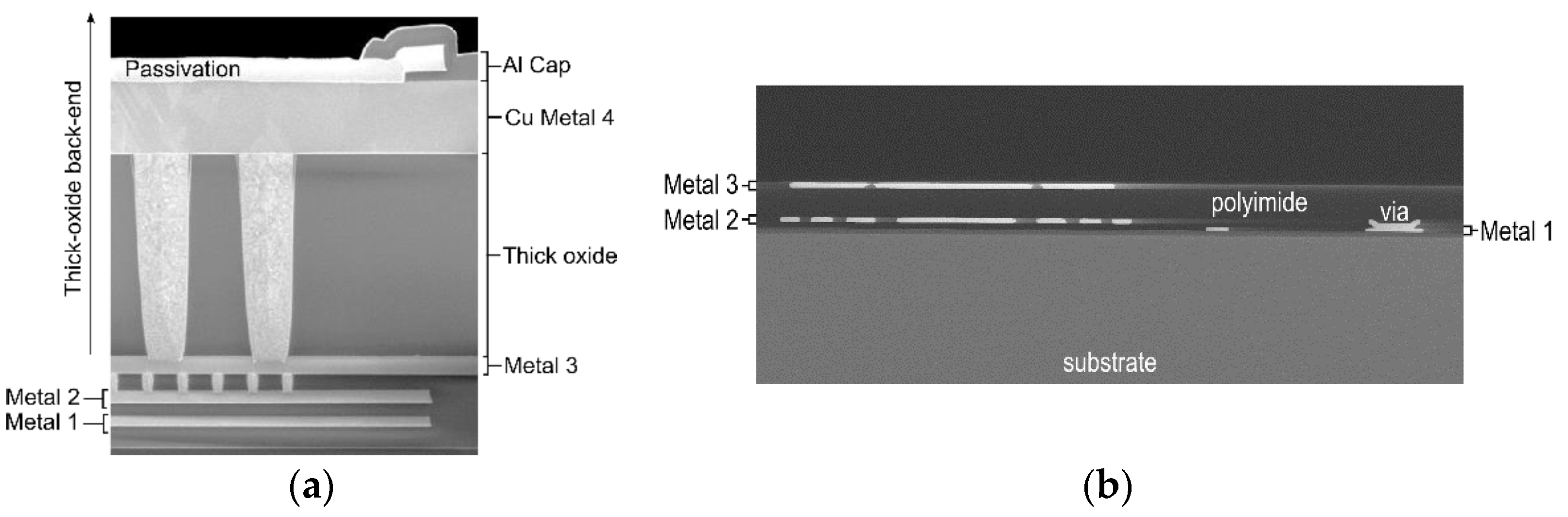
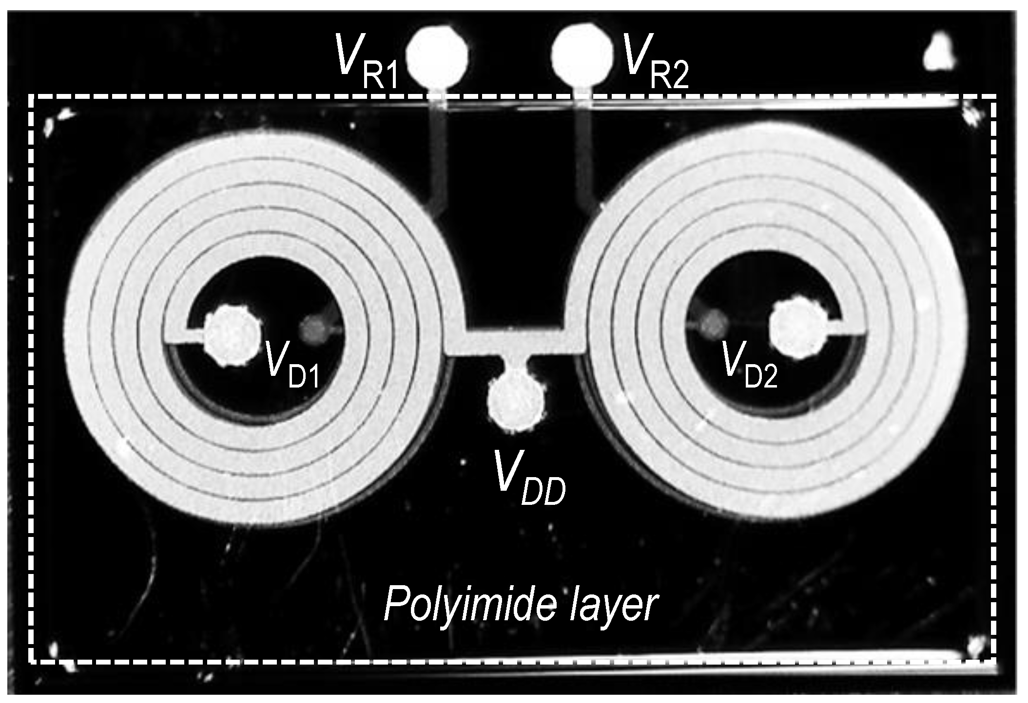
3.1. Integrated Isolation Transformers
3.2. Stand-Alone Isolation Transformers
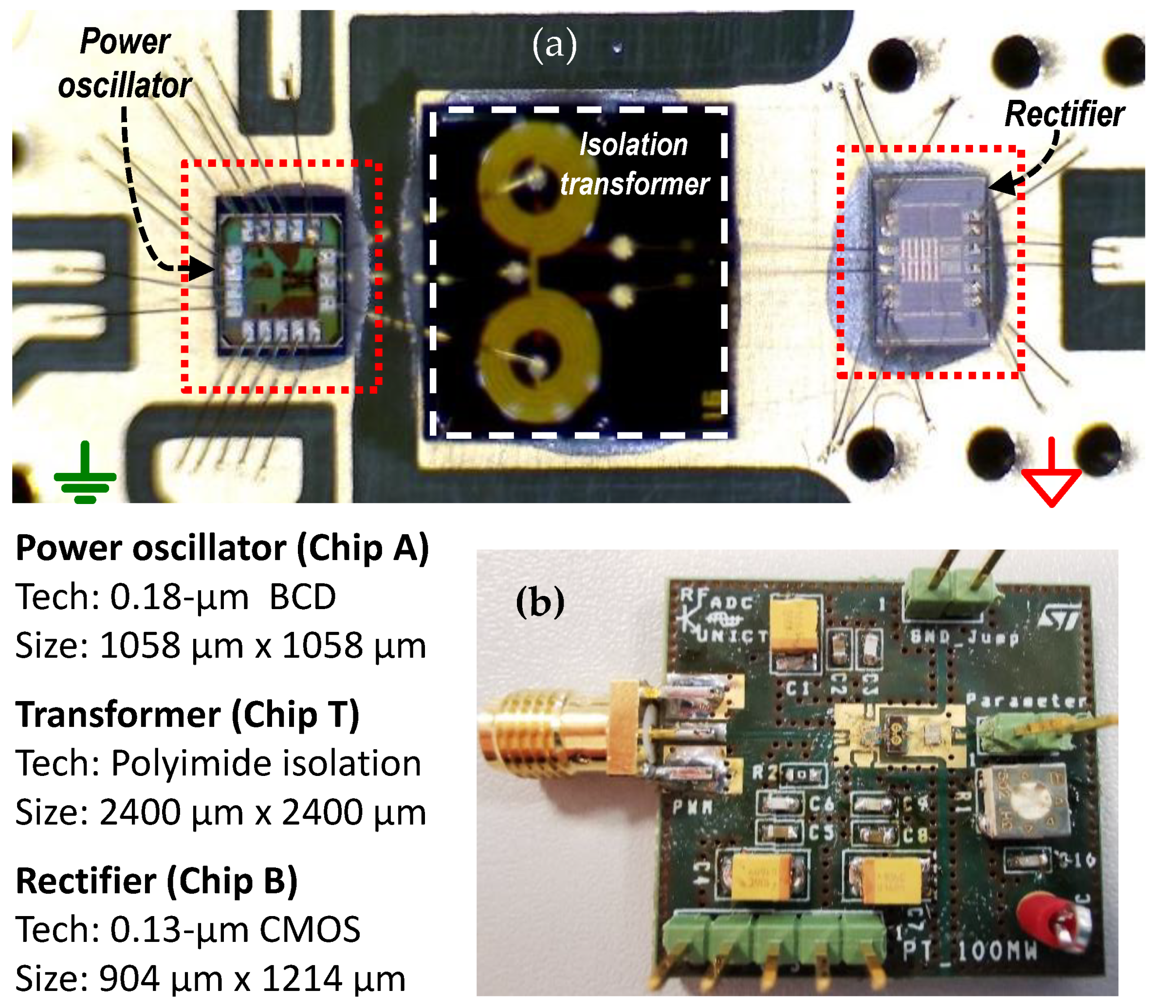
4. Experimental Comparison
5. Conclusions
Author Contributions
Funding
Data Availability Statement
Acknowledgments
Conflicts of Interest
References
- Ragonese, E.; Parisi, A.; Spina, N.; Palmisano, G. Fully integrated galvanically isolated DC-DC converters based on inductive coupling. In International Conference on Applications in Electronics Pervading Industry, Environment and Society; Springer International Publishing: Cham, Switzerland, 2019; pp. 335–341. [Google Scholar]
- Lombardo, P.; Fiore, V.; Ragonese, E.; Palmisano, G. A fully-integrated half-duplex data/power transfer system with up to 40Mbps data rate, 23mW output power and on-chip 5kV galvanic isolation. In Proceedings of the IEEE Int. Solid-State Circuits Conference. Dig. Tech. Papers (ISCCC), San Francisco, CA, USA, 31 January–4 February 2016; pp. 300–301. [Google Scholar]
- Qin, W.; Yang, X.; Ma, S.; Liu, F.; Zhao, Y.; Zhao, T.; Chen, B. An 800mW fully integrated galvanic isolated power transfer system meeting CISPR 22 Class-B emission levels with 6dB margin. In Proceedings of the IEEE International Solid-State Circuits Conference. Dig. Tech. Papers (ISSCC), San Francisco, CA, USA, 17–21 February 2019; pp. 246–248. [Google Scholar]
- Devices-Magnetic, D.V.S. DIN VDE Semiconductor Devices-Magnetic and Capacitive Coupler for Basic and Reinforced Isolation; VDE Verlag VDE V 0884-11: Berlin, Germany, 1 January 2017. [Google Scholar]
- Greco, N.; Parisi, A.; Lombardo, P.; Spina, N.; Ragonese, E.; Palmisano, G. A double-isolated DC-DC converter based on integrated LC resonant barriers. IEEE Trans. Circuits Syst. I Regul. Pap. 2018, 65, 4423–4433. [Google Scholar] [CrossRef]
- Yun, R.; Sun, J.; Gaalaas, E.; Chen, B. A transformer-based digital isolator with 20kVPK surge capability and > 200kV/µS common mode transient immunity. In Proceedings of the IEEE Symposium. on VLSI Circuits, Honolulu, HI, USA, 15–17 June 2016; pp. 1–2. [Google Scholar]
- Parisi, A.; Ragonese, E.; Spina, N.; Palmisano, G. Galvanically isolated DC-DC converter using a single isolation transformer for multi-channel communication. IEEE Trans. Circuits Syst. I Regul. Pap. 2020, 67, 4434–4444. [Google Scholar] [CrossRef]
- Palumbo, V.; Ghidini, G.; Carollo, E.; Toia, F. Integrated Transformer. U.S. Patent 10236115B2, 19 March 2019. [Google Scholar]
- Ragonese, E.; Spina, N.; Castorina, A.; Lombardo, P.; Greco, N.; Parisi, A.; Palmisano, G. A fully integrated galvanically isolated DC-DC converter with data communication. IEEE Trans. Circuits Syst. I Regul. Pap. 2018, 65, 1432–1441. [Google Scholar] [CrossRef]
- Chen, B. High Frequency Power Converter Based on Transformers. U.S. Patent 7983059B2, 19 July 2011. [Google Scholar]
- Chen, B. Fully integrated isolated DC-DC converter using microtransformers. In Proceedings of the 2008 Twenty-Third Annual IEEE Applied Power Electronics Conference and Exposition, Austin, TX, USA, 24–28 February 2008; pp. 335–338. [Google Scholar]
- Fanori, L.; Andreani, P. Class-D CMOS oscillators. IEEE J. Solid State Circuits 2013, 48, 3105–3119. [Google Scholar] [CrossRef]
- Fiore, V.; Ragonese, E.; Palmisano, G. A fully-integrated watt-level power transfer system with on-chip galvanic isolation in silicon technology. IEEE Trans. Power Electron. 2017, 32, 1984–1995. [Google Scholar] [CrossRef]
- Moscatelli, A.; Merlini, A.; Croce, G.; Galbiati, P.; Contiero, C. LDMOS implementation in a 0.35 μm BCD technology (BCD6). In Proceedings of the International Symposium on Power Semiconductor Devices & IC’s (ISPSD), Toulouse, France, 22–25 May 2000; pp. 323–326. [Google Scholar]
- Riccardi, D.; Causio, A.; Filippi, I.; Paleari, A.; Pregnolato, L.V.; Galbiati, P.; Contiero, C. BCD8 from 7V to 70V: A new 0.l8μm technology platform to address the evolution of applications towards smart power IC’s with high logic contents. In Proceedings of the 19th International Symposium on Power Semiconductor Devices and ICs, Jeju, Korea, 27–31 May 2007; pp. 73–76. [Google Scholar]
- Ragonese, E.; Fiore, V.; Spina, N.; Palmisano, G. Power Oscillator Apparatus with Transformer-Based Power Combining. U.S. Patent 9240752 B2, 19 January 2016. [Google Scholar]
- Spina, N.; Fiore, V.; Lombardo, P.; Ragonese, E.; Palmisano, G. Current-reuse transformer coupled oscillators with output power combining for galvanically isolated power transfer systems. IEEE Trans. Circuits Syst. I Regul. Pap. 2015, 62, 2940–2948. [Google Scholar] [CrossRef]
- Greco, N.; Spina, N.; Fiore, V.; Ragonese, E.; Palmisano, G. A galvanically isolated DC-DC converter based on current-reuse hybrid coupled oscillators. IEEE Trans. Circuits Syst. II Exp. Briefs 2017, 64, 56–60. [Google Scholar] [CrossRef]
- Greco, N.; Parisi, A.; Spina, N.; Ragonese, E.; Palmisano, G. Scalable lumped models of integrated transformers for galvanically isolated power transfer systems. Elsevier Integr. VLSI J. 2018, 63, 323–331. [Google Scholar] [CrossRef]
- Chen, B. Isolated half-bridge gate driver with integrated high-side supply. In Proceedings of the 2008 IEEE Power Electronics Specialists Conference, Rhodes, Greece, 15–19 June 2008; pp. 3615–3618. [Google Scholar]
- Biondi, T.; Scuderi, A.; Ragonese, E.; Palmisano, G. Analysis and modeling of layout scaling in silicon integrated stacked transformers. IEEE Trans. Microw. Theory Tech. 2006, 54, 2203–2210. [Google Scholar] [CrossRef]
- Zhuo, Y.; Ma, S.; Zhao, T.; Qin, W.; Zhao, Y.; Guo, Y.; Yan, H.; Chen, B. A 52% peak efficiency> 1-W isolated power transfer system using fully integrated transformer with magnetic core. IEEE J. Solid State Circuits 2019, 54, 3326–3335. [Google Scholar] [CrossRef]


| Layer | Permittivity, εR | Loss Tangent | Conductivity S/m |
|---|---|---|---|
| Metals | - | - | 3.8 × 10⁷ |
| Polyimide | 3 | <0.01 | - |
| Silicon substrate | 11.7 | - | 0.6 |
| Transformer Windings | MTL No. | t (µm) | n | w (µm) | s (µm) | dOUT (µm) |
|---|---|---|---|---|---|---|
| Primary | 3 | 5 | 4.5 | 53 | 8.5 | 1012 |
| Secondary | 2 | 5 | 12 | 15.5 | 8.5 | 1012 |
| Transformer Winding | Inductance (nH) | Q-Factor | k | Self-Resonance Frequency (MHz) |
|---|---|---|---|---|
| Primary | 32 | 11.6 | 0.81 | 840 |
| Secondary | 239 | 9.1 |
| Refs. | [13] | [18] | [19] | [20] | This Work |
|---|---|---|---|---|---|
| Isolation | Thick oxide | Polyimide | Polyimide | ||
| Isolation transformer BEOL | 3.7-µm Cu 0.9-µm Al | 6-μm Au 6-μm Au | 5-μm Au 5-μm Au | ||
| Isolation transformer substrate | BCD SOI | Low conductivity | Low conductivity | ||
| Chip no. | 2 | 3 | 3 | ||
| Oscillator topology | LDMOS D-class | CMOS CR inductively coupled | CMOS CR hybrid-coupled | HV CMOS D-class | LDMOS D-class |
| Rectifier topology | Schottky diode full bridge | ||||
| POUT (mW) | 780 | 200 | 300 | 225 | 200 |
| η (%) | 28 | 27 | 24 | 25 | 24.5 |
| VDD/VOUT (V) | 5/20 | 5/8 | 5/10 | 5/15 | 5/20 |
| fOSC (MHz) | 165 | 240 | 225 | 160 | 250 |
| Power density (mW/mm2) | 83 | 19 | 36 | n.a. | 25 |
| Isolation Transformer Technology | Simulation | Measurement | Unit | ||||||
|---|---|---|---|---|---|---|---|---|---|
| ηOSC | ηB1 | ηTRAF | ηB2 | ηRECT | η | η | |||
| [13] 1 | On-chip thick oxide | 75.5 | 90 | 52.6 | - | 85.5 | 30.6 | 28 | [%] |
| [18] | On-chip thick oxide | 73 | 90 | 50 | - | 75 | 24.6 | 24 | [%] |
| This work | Standalone polyimide | 58 | 90 | 60 | 90 | 90 | 25.4 | 24.5 | [%] |
Publisher’s Note: MDPI stays neutral with regard to jurisdictional claims in published maps and institutional affiliations. |
© 2021 by the authors. Licensee MDPI, Basel, Switzerland. This article is an open access article distributed under the terms and conditions of the Creative Commons Attribution (CC BY) license (https://creativecommons.org/licenses/by/4.0/).
Share and Cite
Ragonese, E.; Spina, N.; Parisi, A.; Palmisano, G. An Experimental Comparison of Galvanically Isolated DC-DC Converters: Isolation Technology and Integration Approach. Electronics 2021, 10, 1186. https://doi.org/10.3390/electronics10101186
Ragonese E, Spina N, Parisi A, Palmisano G. An Experimental Comparison of Galvanically Isolated DC-DC Converters: Isolation Technology and Integration Approach. Electronics. 2021; 10(10):1186. https://doi.org/10.3390/electronics10101186
Chicago/Turabian StyleRagonese, Egidio, Nunzio Spina, Alessandro Parisi, and Giuseppe Palmisano. 2021. "An Experimental Comparison of Galvanically Isolated DC-DC Converters: Isolation Technology and Integration Approach" Electronics 10, no. 10: 1186. https://doi.org/10.3390/electronics10101186