
Low-Toxicity Perovskite Applications in Carbon Electrode Perovskite Solar Cells—A Review


Abstract
:1. Introduction
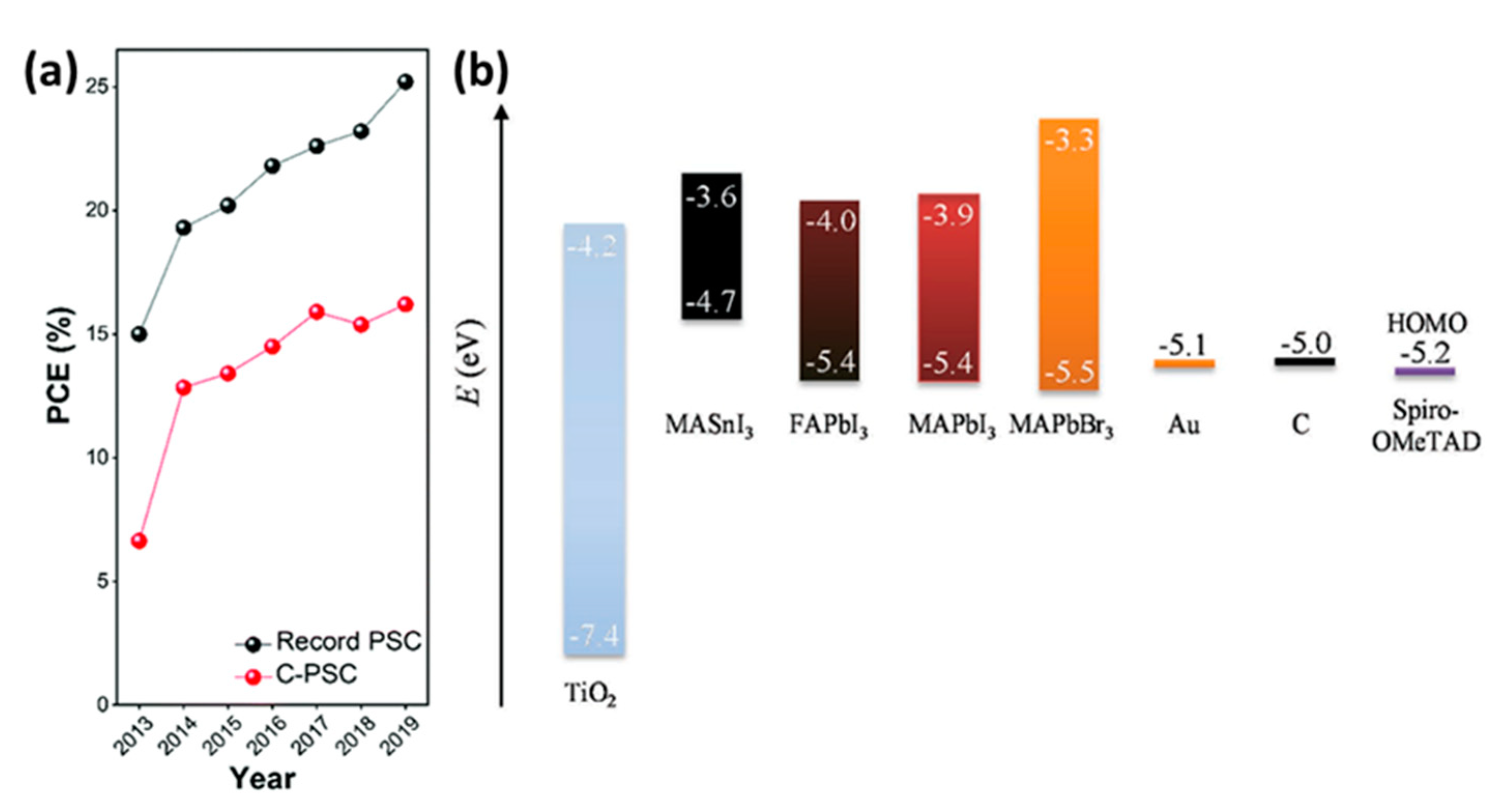
2. Carbon-Based Perovskite Solar Cells (C-PSCs)
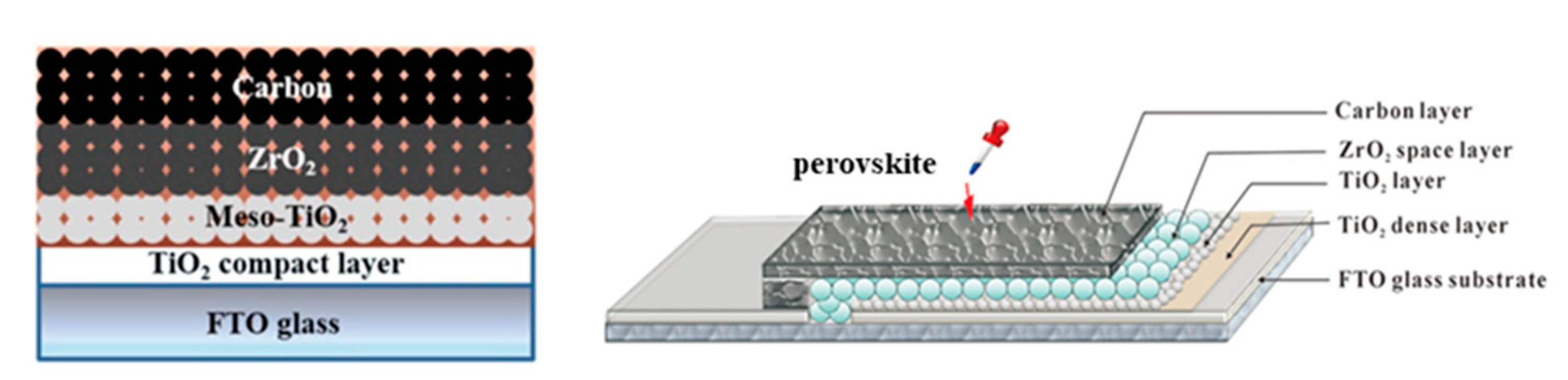
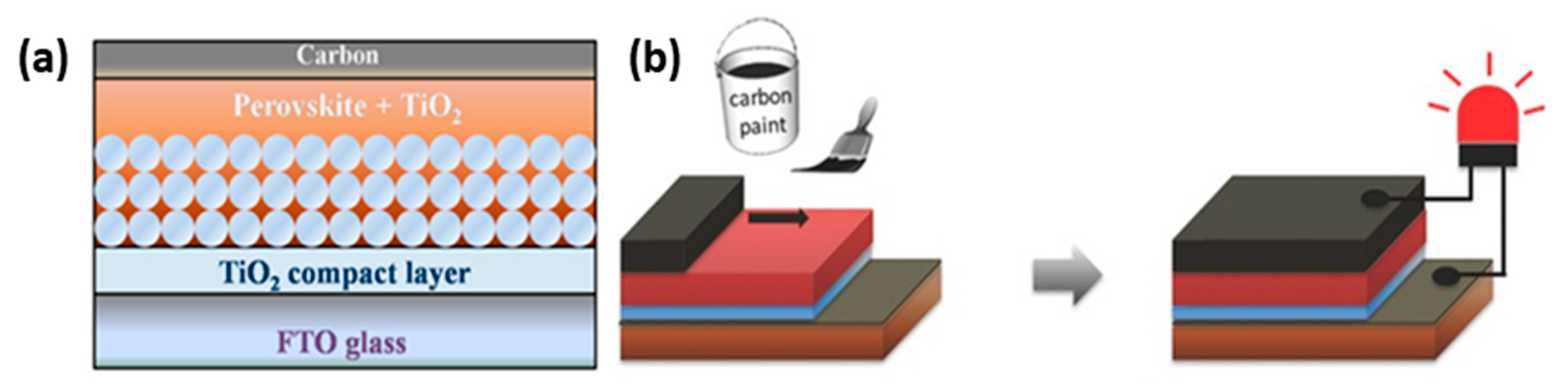
2.1. General Description
2.2. High-Temperature (HT) C-PSCs
2.3. Low-Temperature (LT) C-PSCs
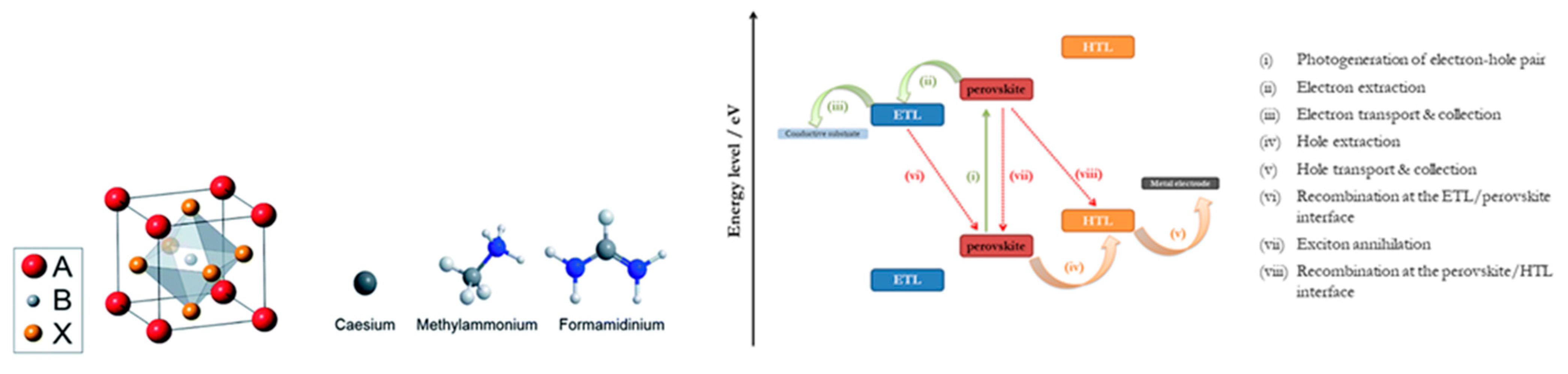
3. Perovskites
3.1. General Description-Current State of the Art
- Tin (Sn)
- Germanium (Ge)
- Bismuth (Bi)
- Antimony (Sb)
- Copper (Cu)
3.2. Pb-Free Perovskites in C-PSCs
3.2.1. Tin (Sn)-Based Perovskites
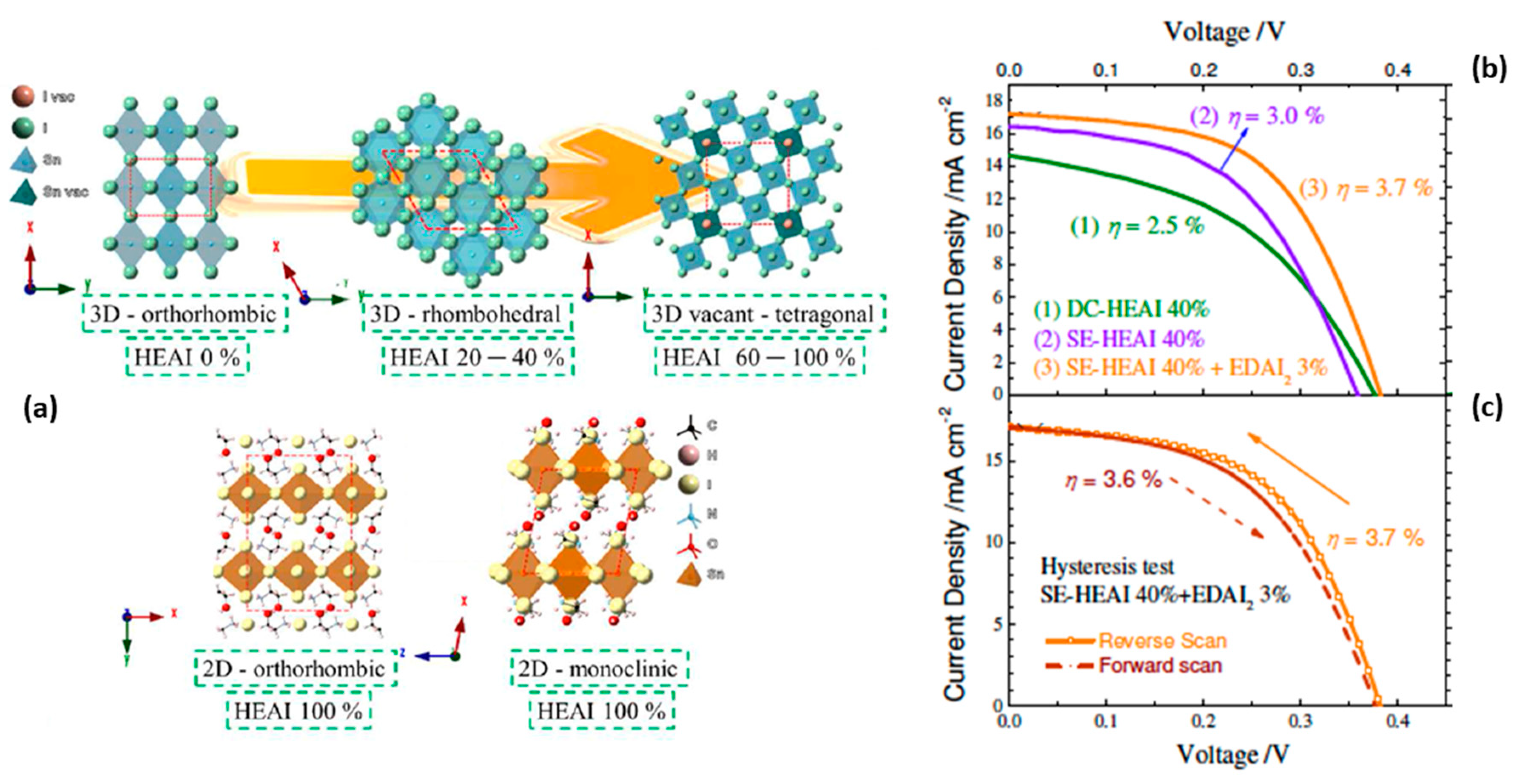
Hybrid Organic-Inorganic (HOI) Sn-Based Perovskites
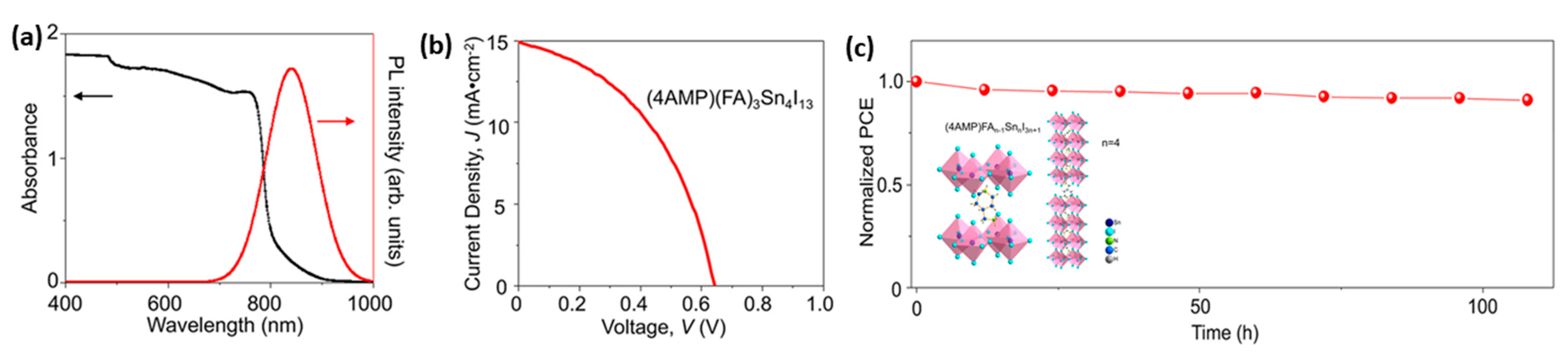
Reduced-Dimensionality HOI Sn-Based Perovskites
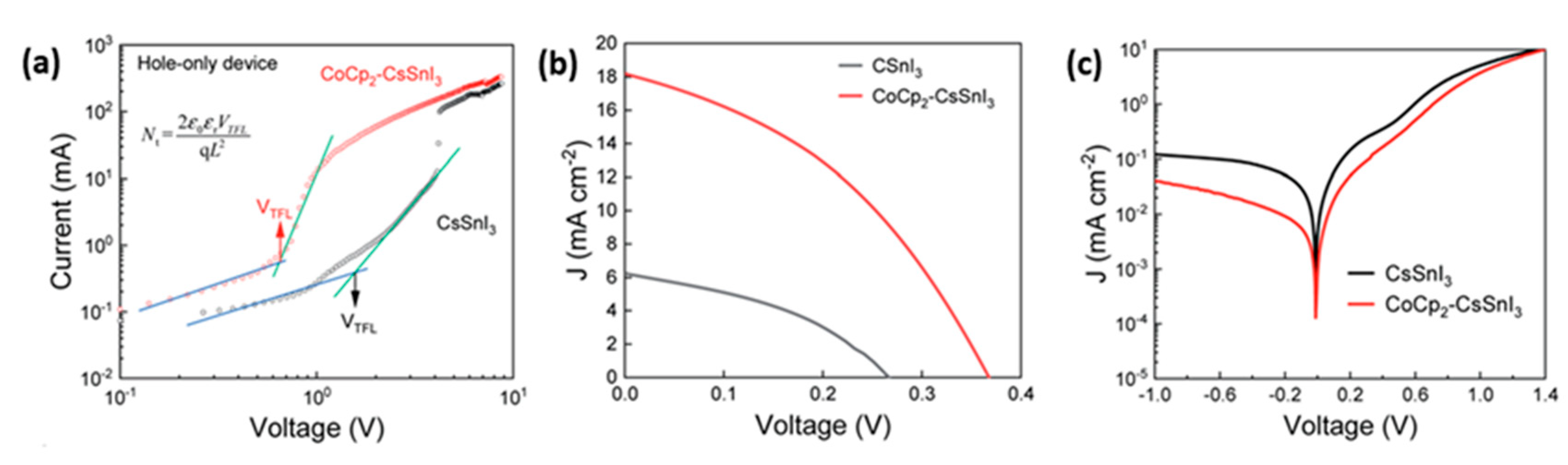
Inorganic Sn-Based Perovskites
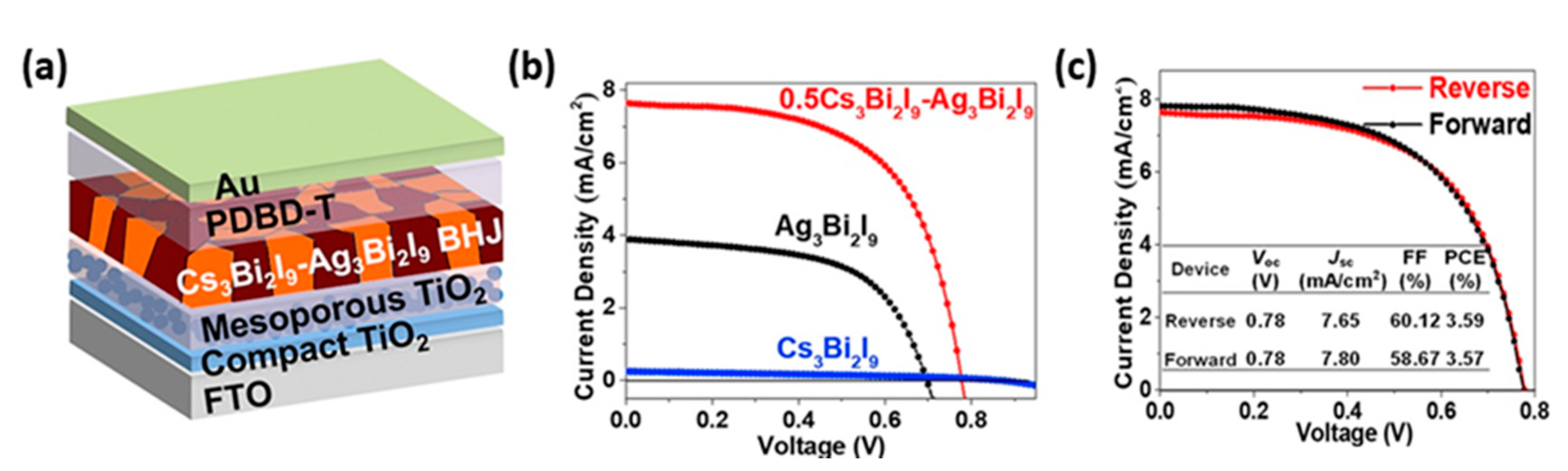
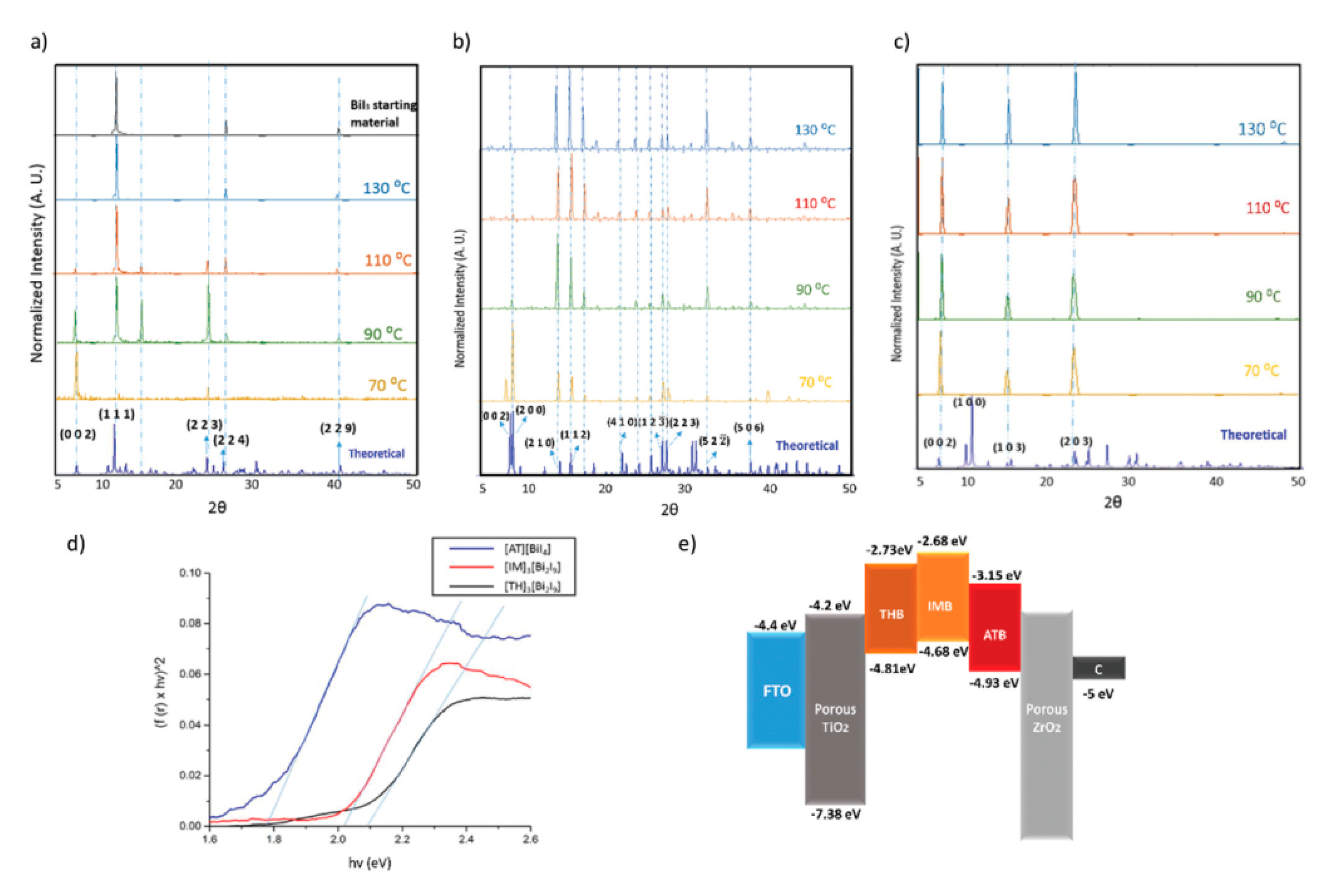
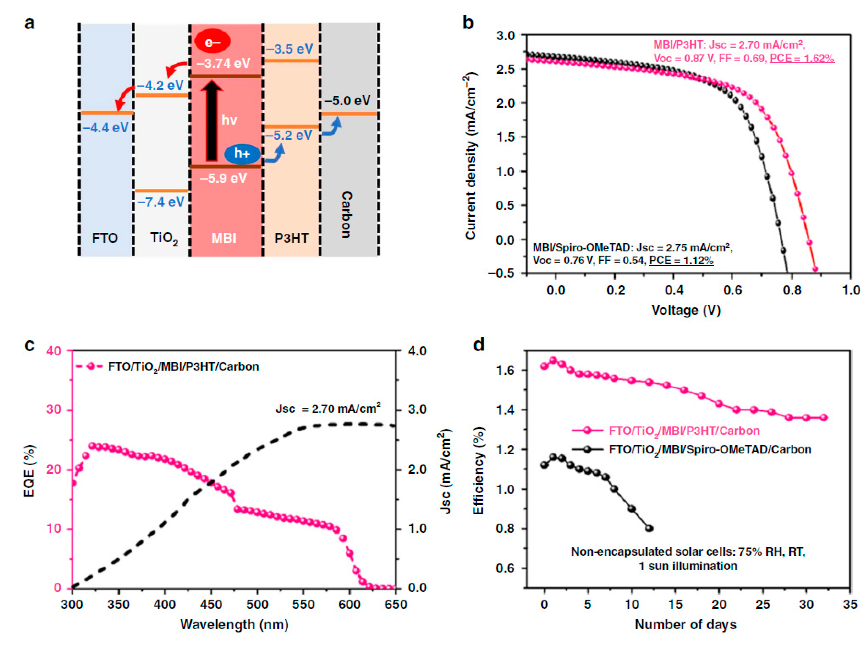
3.2.2. Bismuth Based Perovskites
3.2.3. Antimony Based Perovskites
3.2.4. Other Structures
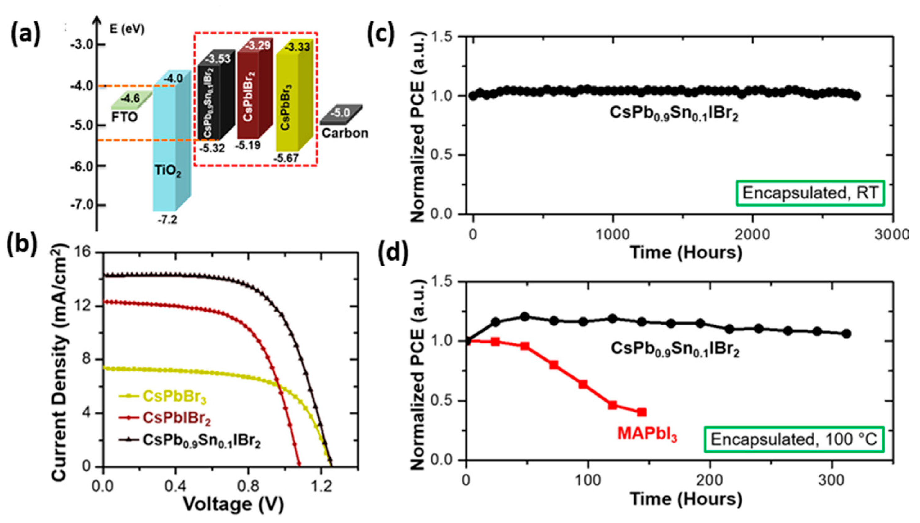
3.3. Low-Toxicity Mixed X-Pb Perovskites in C-PSCs
4. Conclusions
Author Contributions
Funding
Conflicts of Interest
References
- Mitzi, D.B. Templating and structural engineering in organic–inorganic perovskites. J. Chem. Soc. Dalt. Trans. 2001, 1–12. [Google Scholar] [CrossRef]
- Mitzi, D.B. Synthesis, Structure, and Properties of Organic-Inorganic Perovskites and Related Materials. Prog. Inorg. Chem. 1999, 48, 1–121. [Google Scholar]
- Best Research-Cell Efficiency Chart. Available online: https://www.nrel.gov/pv/cell-efficiency.html (accessed on 9 May 2021).
- Bidikoudi, M.; Fresta, E.; Costa, R.D. White perovskite based lighting devices. Chem. Commun. 2018, 54, 8150–8169. [Google Scholar] [CrossRef] [PubMed]
- Miao, J.; Zhang, F. Recent progress on highly sensitive perovskite photodetectors. J. Mater. Chem. C 2019, 7, 1741–1791. [Google Scholar] [CrossRef]
- Stylianakis, M.M.; Maksudov, T.; Panagiotopoulos, A.; Kakavelakis, G.; Petridis, K. Inorganic and Hybrid Perovskite Based Laser Devices: A Review. Materials 2019, 12, 859. [Google Scholar] [CrossRef] [Green Version]
- Atta, N.F. Perovskite Nanomaterials—Synthesis, Characterization, and Applications; Galal, A., Ed.; IntechOpen: Rijeka, Croatia, 2016. [Google Scholar]
- Takano, Y.; Kimishima, Y.; Taketomi, H.; Ogawa, S.; Takayanagi, S.; Môri, N. New Copper-Free Layered Perovskite Superconductors: KCa2Nb3O10 and Related Compounds BT—Stripes and Related Phenomena; Bianconi, A., Saini, N.L., Eds.; Springer: Boston, MA, USA, 2000; pp. 573–578. ISBN 978-0-306-47100-1. [Google Scholar]
- Park, N.-G.; Zhu, K. Scalable fabrication and coating methods for perovskite solar cells and solar modules. Nat. Rev. Mater. 2020, 5, 333–350. [Google Scholar] [CrossRef]
- Zhao, Y.; Ma, F.; Gao, F.; Yin, Z.; Zhang, X.; You, J. Research progress in large-area perovskite solar cells. Photonics Res. 2020, 8, A1–A15. [Google Scholar] [CrossRef]
- Wali, Q.; Iftikhar, F.J.; Khan, M.E.; Ullah, A.; Iqbal, Y.; Jose, R. Advances in stability of perovskite solar cells. Org. Electron. 2020, 78, 105590. [Google Scholar] [CrossRef]
- Berhe, T.A.; Su, W.-N.; Chen, C.-H.; Pan, C.-J.; Cheng, J.-H.; Chen, H.-M.; Tsai, M.-C.; Chen, L.-Y.; Dubale, A.A.; Hwang, B.-J. Organometal halide perovskite solar cells: Degradation and stability. Energy Environ. Sci. 2016, 9, 323–356. [Google Scholar] [CrossRef]
- Wang, J.; Chen, X.; Jiang, F.; Luo, Q.; Zhang, L.; Tan, M.; Xie, M.; Li, Y.-Q.; Zhou, Y.; Su, W.; et al. Electrochemical Corrosion of Ag Electrode in the Silver Grid Electrode-Based Flexible Perovskite Solar Cells and the Suppression Method. Sol. RRL 2018, 2, 1800118. [Google Scholar] [CrossRef]
- Grancini, G.; Roldán-Carmona, C.; Zimmermann, I.; Mosconi, E.; Lee, X.; Martineau, D.; Narbey, S.; Oswald, F.; De Angelis, F.; Graetzel, M.; et al. One-Year stable perovskite solar cells by 2D/3D interface engineering. Nat. Commun. 2017, 8, 1–8. [Google Scholar] [CrossRef]
- Hadadian, M.; Smått, J.-H.; Correa-Baena, J.-P. The role of carbon-based materials in enhancing the stability of perovskite solar cells. Energy Environ. Sci. 2020, 13, 1377–1407. [Google Scholar] [CrossRef]
- Chen, H.; Yang, S. Carbon-Based Perovskite Solar Cells without Hole Transport Materials: The Front Runner to the Market? Adv. Mater. 2017, 29, 1603994. [Google Scholar] [CrossRef]
- Cai, Y.; Liang, L.; Gao, P. Promise of commercialization: Carbon materials for low-cost perovskite solar cells. Chin. Phys. B 2018, 27, 018805. [Google Scholar] [CrossRef] [Green Version]
- Ku, Z.; Rong, Y.; Xu, M.; Liu, T.; Han, H. Full Printable Processed Mesoscopic CH3NH3PbI3/TiO2 Heterojunction Solar Cells with Carbon Counter Electrode. Sci. Rep. 2013, 3, 3132. [Google Scholar] [CrossRef] [PubMed] [Green Version]
- Chen, J.; Xiong, Y.; Rong, Y.; Mei, A.; Sheng, Y.; Jiang, P.; Hu, Y.; Li, X.; Han, H. Solvent effect on the hole-conductor-free fully printable perovskite solar cells. Nano Energy 2016, 27, 130–137. [Google Scholar] [CrossRef]
- Kim, B.; Ko, S.G.; Sonu, K.S.; Ri, J.H.; Kim, U.C.; Ryu, G. Il Effects of Adding PbI2 on the Performance of Hole-Transport Material-Free Mesoscopic Perovskite Solar Cells with Carbon Electrode. J. Electron. Mater. 2018, 47, 6266–6271. [Google Scholar] [CrossRef]
- Mei, A.; Li, X.; Liu, L.; Ku, Z.; Liu, T.; Rong, Y.; Xu, M.; Hu, M.; Chen, J.; Yang, Y.; et al. A hole-conductor-free, fully printable mesoscopic perovskite solar cell with high stability. Science 2014, 345, 295–298. [Google Scholar] [CrossRef] [PubMed]
- Li, H.; Cao, K.; Cui, J.; Liu, S.; Qiao, X.; Shen, Y.; Wang, M. 14.7% Efficient Mesoscopic Perovskite Solar Cells Using Single Walled Carbon Nanotubes/Carbon Composite Counter Electrodes. Nanoscale 2016, 8, 6379–6385. [Google Scholar] [CrossRef]
- Yang, Y.; Liu, Z.; Ng, W.K.; Zhang, L.; Zhang, H.; Meng, X.; Bai, Y.; Xiao, S.; Zhang, T.; Hu, C.; et al. An Ultrathin Ferroelectric Perovskite Oxide Layer for High-Performance Hole Transport Material Free Carbon Based Halide Perovskite Solar Cells. Adv. Funct. Mater. 2019, 29, 1806506. [Google Scholar] [CrossRef] [Green Version]
- Liu, S.; Huang, W.; Liao, P.; Pootrakulchote, N.; Li, H.; Lu, J.; Li, J.; Huang, F.; Shai, X.; Zhao, X.; et al. 17% efficient printable mesoscopic PIN metal oxide framework perovskite solar cells using cesium-containing triple cation perovskite. J. Mater. Chem. A 2017, 5, 22952–22958. [Google Scholar] [CrossRef]
- Sheng, Y.; Ji, W.; Chu, Y.; Ming, Y.; Mei, A.; Hu, Y.; Rong, Y.; Han, H. Post-Treatment of Mesoporous Scaffolds for Enhanced Photovoltage of Triple-Mesoscopic Perovskite Solar Cells. Sol. RRL 2020, 4, 2000185. [Google Scholar] [CrossRef]
- Wang, Q.; Zhang, W.; Zhang, Z.; Liu, S.; Wu, J.; Guan, Y.; Mei, A.; Rong, Y.; Hu, Y.; Han, H. Crystallization Control of Ternary-Cation Perovskite Absorber in Triple-Mesoscopic Layer for Efficient Solar Cells. Adv. Energy Mater. 2020, 10, 1903092. [Google Scholar] [CrossRef]
- Zhang, H.; Wang, H.; Williams, S.T.; Xiong, D.; Zhang, W.; Chueh, C.-C.; Chen, W.; Jen, A.K.-Y. SrCl2 Derived Perovskite Facilitating a High Efficiency of 16% in Hole-Conductor-Free Fully Printable Mesoscopic Perovskite Solar Cells. Adv. Mater. 2017, 29, 1606608. [Google Scholar] [CrossRef]
- Li, D.; Tong, C.; Ji, W.; Fu, Z.; Wan, Z.; Huang, Q.; Ming, Y.; Mei, A.; Hu, Y.; Rong, Y.; et al. Vanadium Oxide Post-Treatment for Enhanced Photovoltage of Printable Perovskite Solar Cells. ACS Sustain. Chem. Eng. 2019, 7, 2619–2625. [Google Scholar] [CrossRef]
- Tian, C.; Mei, A.; Zhang, S.; Tian, H.; Liu, S.; Qin, F.; Xiong, Y.; Rong, Y.; Hu, Y.; Zhou, Y.; et al. Oxygen management in carbon electrode for high-performance printable perovskite solar cells. Nano Energy 2018, 53, 160–167. [Google Scholar] [CrossRef]
- Rong, Y.; Hou, X.; Hu, Y.; Mei, A.; Liu, L.; Wang, P.; Han, H. Synergy of ammonium chloride and moisture on perovskite crystallization for efficient printable mesoscopic solar cells. Nat. Commun. 2017, 8. [Google Scholar] [CrossRef]
- Hu, Y.; Zhang, Z.; Mei, A.; Jiang, Y.; Hou, X.; Wang, Q.; Du, K.; Rong, Y.; Zhou, Y.; Xu, G.; et al. Improved Performance of Printable Perovskite Solar Cells with Bifunctional Conjugated Organic Molecule. Adv. Mater. 2018, 30, 1705786. [Google Scholar] [CrossRef]
- Ming, Y.; Xu, M.; Liu, S.; Li, D.; Wang, Q.; Hou, X.; Hu, Y.; Rong, Y.; Han, H. Ethanol stabilized precursors for highly reproducible printable mesoscopic perovskite solar cells. J. Power Sources 2019, 424, 261–267. [Google Scholar] [CrossRef]
- Cao, K.; Zuo, Z.; Cui, J.; Shen, Y.; Moehl, T.; Zakeeruddin, S.M.; Grätzel, M.; Wang, M. Efficient screen printed perovskite solar cells based on mesoscopic TiO2/Al2O3/NiO/carbon architecture. Nano Energy 2015, 17, 171–179. [Google Scholar] [CrossRef]
- Tsai, C.M.; Wu, G.W.; Narra, S.; Chang, H.M.; Mohanta, N.; Wu, H.P.; Wang, C.L.; Diau, E.W.G. Control of preferred orientation with slow crystallization for carbon-based mesoscopic perovskite solar cells attaining efficiency 15%. J. Mater. Chem. A 2017, 5, 739–747. [Google Scholar] [CrossRef]
- Hou, X.; Xu, M.; Tong, C.; Ji, W.; Fu, Z.; Wan, Z.; Hao, F.; Ming, Y.; Liu, S.; Hu, Y.; et al. High performance printable perovskite solar cells based on Cs0.1FA0.9PbI3 in mesoporous scaffolds. J. Power Sources 2019, 415, 105–111. [Google Scholar] [CrossRef]
- Xu, X.; Liu, Z.; Zuo, Z.; Zhang, M.; Zhao, Z.; Shen, Y.; Zhou, H.; Chen, Q.; Yang, Y.; Wang, M. Hole Selective NiO Contact for Efficient Perovskite Solar Cells with Carbon Electrode. Nano Lett. 2015, 15, 2402–2408. [Google Scholar] [CrossRef] [PubMed]
- Jiang, H.; Liu, X.; Chai, N.; Huang, F.; Peng, Y.; Zhong, J.; Zhang, Q.; Ku, Z.; Cheng, Y. Alleviate the J–V hysteresis of carbon-based perovskite solar cells via introducing additional methylammonium chloride into MAPbI3 precursor. RSC Adv. 2018, 8, 35157–35161. [Google Scholar] [CrossRef] [Green Version]
- Sheng, Y.; Hu, Y.; Mei, A.; Jiang, P.; Hou, X.; Duan, M.; Hong, L.; Guan, Y.; Rong, Y.; Xiong, Y.; et al. Enhanced electronic properties in CH3NH3PbI3: Via LiCl mixing for hole-conductor-free printable perovskite solar cells. J. Mater. Chem. A 2016, 4, 16731–16736. [Google Scholar] [CrossRef]
- Hashmi, S.G.; Martineau, D.; Dar, M.I.; Myllymäki, T.T.T.; Sarikka, T.; Ulla, V.; Zakeeruddin, S.M.; Grätzel, M. High performance carbon-based printed perovskite solar cells with humidity assisted thermal treatment. J. Mater. Chem. A 2017, 5, 12060–12067. [Google Scholar] [CrossRef] [Green Version]
- Hou, X.; Hu, Y.; Liu, H.; Mei, A.; Li, X.; Duan, M.; Zhang, G.; Rong, Y.; Han, H. Effect of guanidinium on mesoscopic perovskite solar cells. J. Mater. Chem. A 2017, 5, 73–78. [Google Scholar] [CrossRef]
- Liu, Z.; Zhang, M.; Xu, X.; Cai, F.; Yuan, H.; Bu, L.; Li, W.; Zhu, A.; Zhao, Z.; Wang, M.; et al. NiO nanosheets as efficient top hole transporters for carbon counter electrode based perovskite solar cells. J. Mater. Chem. A 2015, 3, 24121–24127. [Google Scholar] [CrossRef]
- Zhang, F.; Yang, X.; Wang, H.; Cheng, M.; Zhao, J.; Sun, L. Structure engineering of hole-conductor free perovskite-based solar cells with low-temperature-processed commercial carbon paste as cathode. ACS Appl. Mater. Interfaces 2014, 6, 16140–16146. [Google Scholar] [CrossRef] [PubMed]
- Chen, H.; Wei, Z.; He, H.; Zheng, X.; Wong, K.S.; Yang, S. Solvent Engineering Boosts the Efficiency of Paintable Carbon-Based Perovskite Solar Cells to Beyond 14%. Adv. Energy Mater. 2016, 6, 1502087. [Google Scholar] [CrossRef]
- Zhang, H.; Xiao, J.; Shi, J.; Su, H.; Luo, Y.; Li, D.; Wu, H.; Cheng, Y.-B.; Meng, Q. Self-Adhesive Macroporous Carbon Electrodes for Efficient and Stable Perovskite Solar Cells. Adv. Funct. Mater. 2018, 28, 1802985. [Google Scholar] [CrossRef]
- Su, H.; Xiao, J.; Li, Q.; Peng, C.; Zhang, X.; Mao, C.; Yao, Q.; Lu, Y.; Ku, Z.; Zhong, J.; et al. Carbon film electrode based square-centimeter scale planar perovskite solar cells exceeding 17% efficiency. Mater. Sci. Semicond. Process. 2020, 107, 104809. [Google Scholar] [CrossRef]
- Lee, J.-W.; Jeon, I.; Lin, H.-S.; Seo, S.; Han, T.-H.; Anisimov, A.; Kauppinen, E.I.; Matsuo, Y.; Maruyama, S.; Yang, Y. Vapor-Assisted Ex-Situ Doping of Carbon Nanotube toward Efficient and Stable Perovskite Solar Cells. Nano Lett. 2019, 19, 2223–2230. [Google Scholar] [CrossRef] [PubMed]
- Bogachuk, D.; Zouhair, S.; Wojciechowski, K.; Yang, B.; Babu, V.; Wagner, L.; Xu, B.; Lim, J.; Mastroianni, S.; Pettersson, H.; et al. Low-temperature carbon-based electrodes in perovskite solar cells. Energy Environ. Sci. 2020, 13, 3880–3916. [Google Scholar] [CrossRef]
- Zhang, C.; Wang, S.; Zhang, H.; Feng, Y.; Tian, W.; Yan, Y.; Bian, J.; Wang, Y.; Jin, S.; Zakeeruddin, S.M.; et al. Efficient stable graphene-based perovskite solar cells with high flexibility in device assembling via modular architecture design. Energy Environ. Sci. 2019, 12, 3585–3594. [Google Scholar] [CrossRef]
- Chu, Q.-Q.; Ding, B.; Peng, J.; Shen, H.; Li, X.; Liu, Y.; Li, C.-X.; Li, C.-J.; Yang, G.-J.; White, T.P.; et al. Highly stable carbon-based perovskite solar cell with a record efficiency of over 18% via hole transport engineering. J. Mater. Sci. Technol. 2019, 35, 987–993. [Google Scholar] [CrossRef]
- Arora, N.; Dar, M.I.; Akin, S.; Uchida, R.; Baumeler, T.; Liu, Y.; Zakeeruddin, S.M.; Grätzel, M. Low-Cost and Highly Efficient Carbon-Based Perovskite Solar Cells Exhibiting Excellent Long-Term Operational and UV Stability. Small 2019, 15, 1904746. [Google Scholar] [CrossRef] [PubMed]
- Ye, H.; Liu, Z.; Liu, X.; Sun, B.; Tan, X.; Tu, Y.; Shi, T.; Tang, Z.; Liao, G. 17.78% efficient low-temperature carbon-based planar perovskite solar cells using Zn-doped SnO2 electron transport layer. Appl. Surf. Sci. 2019, 478, 417–425. [Google Scholar] [CrossRef]
- Wu, X.; Xie, L.; Lin, K.; Lu, J.; Wang, K.; Feng, W.; Fan, B.; Yin, P.; Wei, Z. Efficient and stable carbon-based perovskite solar cells enabled by the inorganic interface of CuSCN and carbon nanotubes. J. Mater. Chem. A 2019, 7, 12236–12243. [Google Scholar] [CrossRef]
- Liu, X.; Liu, Z.; Sun, B.; Tan, X.; Ye, H.; Tu, Y.; Shi, T.; Tang, Z.; Liao, G. 17.46% efficient and highly stable carbon-based planar perovskite solar cells employing Ni-doped rutile TiO2 as electron transport layer. Nano Energy 2018, 50, 201–211. [Google Scholar] [CrossRef]
- Kerttu, A.; Konrad, D.; Juan-Pablo, C.; Kári, S.; Michael, S.; Antonio, A.; Michael, G.; Esko, K.; Johansson, J.E.M.; Wolfgang, T.; et al. High Temperature-Stable Perovskite Solar Cell Based on Low-Cost Carbon Nanotube Hole Contact. Adv. Mater. 2017, 29, 1606398. [Google Scholar] [CrossRef]
- Zhou, J.; Wu, J.; Li, N.; Li, X.; Zheng, Y.-Z.; Tao, X. Efficient all-air processed mixed cation carbon-based perovskite solar cells with ultra-high stability. J. Mater. Chem. A 2019, 7, 17594–17603. [Google Scholar] [CrossRef]
- Liu, J.; Zhou, Q.; Thein, N.K.; Tian, L.; Jia, D.; Johansson, E.M.J.; Zhang, X. In situ growth of perovskite stacking layers for high-efficiency carbon-based hole conductor free perovskite solar cells. J. Mater. Chem. A 2019, 7, 13777–13786. [Google Scholar] [CrossRef]
- Zhang, F.; Yang, X.; Cheng, M.; Wang, W.; Sun, L. Boosting the efficiency and the stability of low cost perovskite solar cells by using CuPc nanorods as hole transport material and carbon as counter electrode. Nano Energy 2016, 20, 108–116. [Google Scholar] [CrossRef]
- Zhou, J.; Hou, J.; Tao, X.; Meng, X.; Yang, S. Solution-processed electron transport layer of n-doped fullerene for efficient and stable all carbon based perovskite solar cells. J. Mater. Chem. A 2019, 7, 7710–7716. [Google Scholar] [CrossRef]
- Wang, Y.; Zhao, H.; Mei, Y.; Liu, H.; Wang, S.; Li, X. Carbon Nanotube Bridging Method for Hole Transport Layer-Free Paintable Carbon-Based Perovskite Solar Cells. ACS Appl. Mater. Interfaces 2019, 11, 916–923. [Google Scholar] [CrossRef] [PubMed]
- Lee, K.; Kim, J.; Yu, H.; Lee, J.W.; Yoon, C.-M.; Kim, S.K.; Jang, J. A highly stable and efficient carbon electrode-based perovskite solar cell achieved via interfacial growth of 2D PEA2PbI4 perovskite. J. Mater. Chem. A 2018, 6, 24560–24568. [Google Scholar] [CrossRef]
- Meng, X.; Zhou, J.; Hou, J.; Tao, X.; Cheung, S.H.; So, S.K.; Yang, S. Versatility of Carbon Enables All Carbon Based Perovskite Solar Cells to Achieve High Efficiency and High Stability. Adv. Mater. 2018, 30, 1706975. [Google Scholar] [CrossRef] [PubMed]
- Gholipour, S.; Correa-Baena, J.-P.; Domanski, K.; Matsui, T.; Steier, L.; Giordano, F.; Tajabadi, F.; Tress, W.; Saliba, M.; Abate, A.; et al. Highly Efficient and Stable Perovskite Solar Cells based on a Low-Cost Carbon Cloth. Adv. Energy Mater. 2016, 6, 1601116. [Google Scholar] [CrossRef]
- Liu, T.; Wang, Z.; Lou, L.; Xiao, S.; Zheng, S.; Yang, S. Interfacial Post-Treatment for Enhancing the Performance of Printable Carbon-Based Perovskite Solar Cells. Sol. RRL 2020, 4, 1900278. [Google Scholar] [CrossRef]
- Zheng, X.; Chen, H.; Li, Q.; Yang, Y.; Wei, Z.; Bai, Y.; Qiu, Y.; Zhou, D.; Wong, K.S.; Yang, S. Boron Doping of Multiwalled Carbon Nanotubes Significantly Enhances Hole Extraction in Carbon-Based Perovskite Solar Cells. Nano Lett. 2017, 17, 2496–2505. [Google Scholar] [CrossRef] [PubMed]
- Eperon, G.E.; Stranks, S.D.; Menelaou, C.; Johnston, M.B.; Herz, L.M.; Snaith, H.J. Formamidinium lead trihalide: A broadly tunable perovskite for efficient planar heterojunction solar cells. Energy Environ. Sci. 2014, 7, 982–988. [Google Scholar] [CrossRef]
- Kojima, A.; Teshima, K.; Shirai, Y.; Miyasaka, T. Organometal Halide Perovskites as Visible-Light Sensitizers for Photovoltaic Cells. J. Am. Chem. Soc. 2009, 131, 6050–6051. [Google Scholar] [CrossRef] [PubMed]
- Tandem Solar Cells with High Power Conversion Efficiency. Available online: https://www.polyu.edu.hk/cpa/milestones/en/201609/research_innovation/technology/tandem_solar_cells_with_high_power_conversion_effi/index.html (accessed on 11 May 2021).
- World Health Organization Exposure to Lead: A Major Public Health Concern. 2010. Available online: https://apps.who.int/iris/handle/10665/329953 (accessed on 30 April 2021).
- Wolman, A. Public health and environment. Am. J. Public Health 1985, 75, 1049–1051. [Google Scholar] [CrossRef]
- Kour, R.; Arya, S.; Verma, S.; Gupta, J.; Bandhoria, P.; Bharti, V.; Datt, R.; Gupta, V. Potential Substitutes for Replacement of Lead in Perovskite Solar Cells: A Review. Glob. Chall. 2019, 3, 1900050. [Google Scholar] [CrossRef] [Green Version]
- Miyasaka, T.; Kulkarni, A.; Kim, G.M.; Öz, S.; Jena, A.K. Perovskite Solar Cells: Can We Go Organic-Free, Lead-Free, and Dopant-Free? Adv. Energy Mater. 2020, 10, 1902500. [Google Scholar] [CrossRef]
- Hoefler, S.F.; Trimmel, G.; Rath, T. Progress on lead-free metal halide perovskites for photovoltaic applications: A review. Monatshefte Chem. 2017, 148, 795–826. [Google Scholar] [CrossRef] [Green Version]
- Huang, L.; Lambrecht, W.R.L. Electronic band structure, phonons, and exciton binding energies of halide perovskites CsSnCl3, CsSnBr3, and CsSnI3. Phys. Rev. B 2013, 88, 165203. [Google Scholar] [CrossRef]
- Nishimura, K.; Kamarudin, M.A.; Hirotani, D.; Hamada, K.; Shen, Q.; Iikubo, S.; Minemoto, T.; Yoshino, K.; Hayase, S. Lead-free tin-halide perovskite solar cells with 13% efficiency. Nano Energy 2020, 74, 104858. [Google Scholar] [CrossRef]
- Chen, L.-J.; Lee, C.-R.; Chuang, Y.-J.; Wu, Z.-H.; Chen, C. Synthesis and Optical Properties of Lead-Free Cesium Tin Halide Perovskite Quantum Rods with High-Performance Solar Cell Application. J. Phys. Chem. Lett. 2016, 7, 5028–5035. [Google Scholar] [CrossRef] [PubMed]
- Fan, Z.; Sun, K.; Wang, J. Perovskites for photovoltaics: A combined review of organic–inorganic halide perovskites and ferroelectric oxide perovskites. J. Mater. Chem. A 2015, 3, 18809–18828. [Google Scholar] [CrossRef]
- Cao, J.; Yan, F. Recent progress in tin-based perovskite solar cells. Energy Environ. Sci. 2021, 14, 1286–1325. [Google Scholar] [CrossRef]
- Krishnamoorthy, T.; Ding, H.; Yan, C.; Leong, W.L.; Baikie, T.; Zhang, Z.; Sherburne, M.; Li, S.; Asta, M.; Mathews, N.; et al. Lead-free germanium iodide perovskite materials for photovoltaic applications. J. Mater. Chem. A 2015, 3, 23829–23832. [Google Scholar] [CrossRef]
- Liu, Y. The development of low toxic and high efficient solar cells. J. Phys. Conf. Ser. 2020, 1653, 12002. [Google Scholar] [CrossRef]
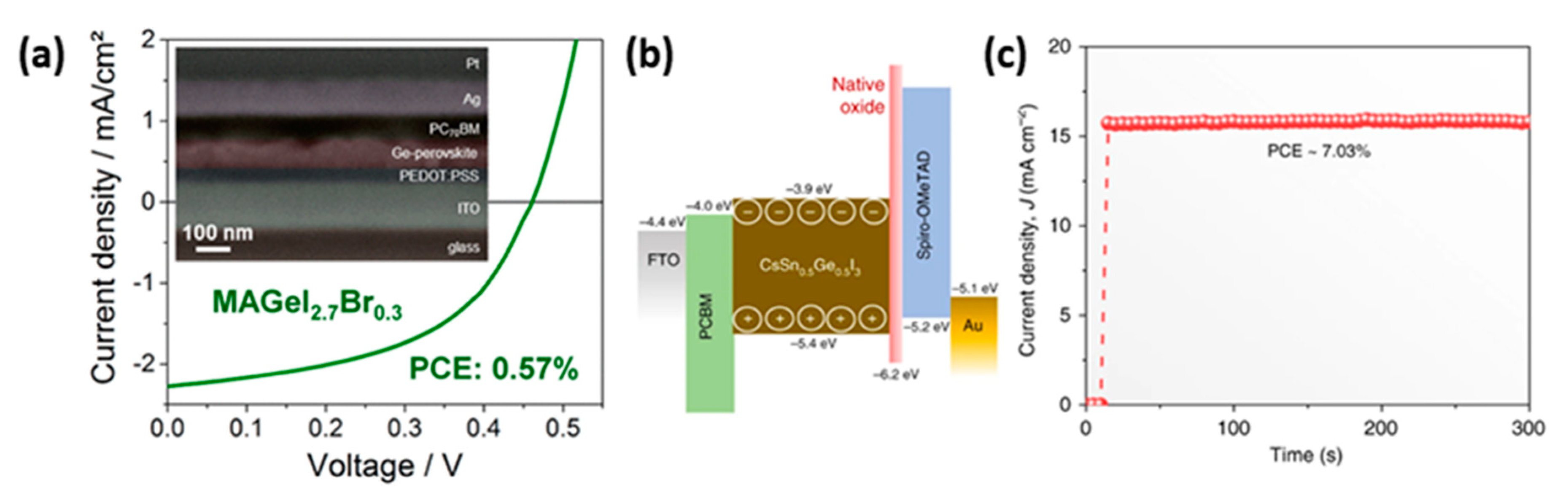
- Kopacic, I.; Friesenbichler, B.; Hoefler, S.F.; Kunert, B.; Plank, H.; Rath, T.; Trimmel, G. Enhanced Performance of Germanium Halide Perovskite Solar Cells through Compositional Engineering. ACS Appl. Energy Mater. 2018, 1, 343–347. [Google Scholar] [CrossRef]
- Chen, M.; Ju, M.-G.; Garces, H.F.; Carl, A.D.; Ono, L.K.; Hawash, Z.; Zhang, Y.; Shen, T.; Qi, Y.; Grimm, R.L.; et al. Highly stable and efficient all-inorganic lead-free perovskite solar cells with native-oxide passivation. Nat. Commun. 2019, 10, 16. [Google Scholar] [CrossRef] [Green Version]
- Öz, S.; Hebig, J.-C.; Jung, E.; Singh, T.; Lepcha, A.; Olthof, S.; Jan, F.; Gao, Y.; German, R.; van Loosdrecht, P.H.M.; et al. Zero-dimensional (CH3NH3)3Bi2I9 perovskite for optoelectronic applications. Sol. Energy Mater. Sol. Cells 2016, 158, 195–201. [Google Scholar] [CrossRef]
- Hu, W.; He, X.; Fang, Z.; Lian, W.; Shang, Y.; Li, X.; Zhou, W.; Zhang, M.; Chen, T.; Lu, Y.; et al. Bulk heterojunction gifts bismuth-based lead-free perovskite solar cells with record efficiency. Nano Energy 2020, 68, 104362. [Google Scholar] [CrossRef]
- Yang, Y.; Liu, C.; Cai, M.; Liao, Y.; Ding, Y.; Ma, S.; Liu, X.; Guli, M.; Dai, S.; Nazeeruddin, M.K. Dimension-Controlled Growth of Antimony-Based Perovskite-like Halides for Lead-Free and Semitransparent Photovoltaics. ACS Appl. Mater. Interfaces 2020, 12, 17062–17069. [Google Scholar] [CrossRef] [PubMed]
- Elseman, A.M.; Shalan, A.E.; Sajid, S.; Rashad, M.M.; Hassan, A.M.; Li, M. Copper-Substituted Lead Perovskite Materials Constructed with Different Halides for Working (CH3NH3)2CuX4-Based Perovskite Solar Cells from Experimental and Theoretical View. ACS Appl. Mater. Interfaces 2018, 10, 11699–11707. [Google Scholar] [CrossRef] [PubMed]
- Liu, C.K.; Tai, Q.; Wang, N.; Tang, G.; Loi, H.L.; Yan, F. Sn-Based Perovskite for Highly Sensitive Photodetectors. Adv. Sci. 2019, 6, 1–8. [Google Scholar] [CrossRef] [PubMed] [Green Version]
- Xie, C.; Liu, C.K.; Loi, H.L.; Yan, F. Perovskite-Based Phototransistors and Hybrid Photodetectors. Adv. Funct. Mater. 2020, 30, 1–28. [Google Scholar] [CrossRef]
- Wang, R.; Wang, J.; Tan, S.; Duan, Y.; Wang, Z.K.; Yang, Y. Opportunities and Challenges of Lead-Free Perovskite Optoelectronic Devices. Trends Chem. 2019, 1, 368–379. [Google Scholar] [CrossRef]
- Shi, Z.; Guo, J.; Chen, Y.; Li, Q.; Pan, Y.; Zhang, H.; Xia, Y.; Huang, W. Lead-Free Organic–Inorganic Hybrid Perovskites for Photovoltaic Applications: Recent Advances and Perspectives. Adv. Mater. 2017, 29. [Google Scholar] [CrossRef]
- Jin, Z.; Zhang, Z.; Xiu, J.; Song, H.; Gatti, T.; He, Z. A critical review on bismuth and antimony halide based perovskites and their derivatives for photovoltaic applications: Recent advances and challenges. J. Mater. Chem. A 2020, 8, 16166–16188. [Google Scholar] [CrossRef]
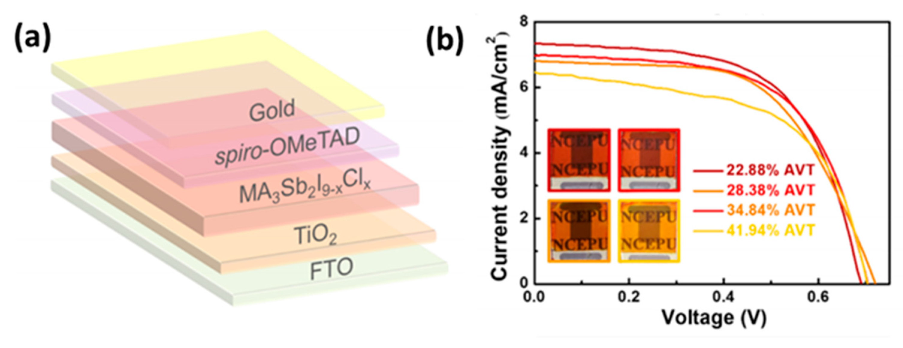
- Umar, F.; Zhang, J.; Jin, Z.; Muhammad, I.; Yang, X.; Deng, H.; Jahangeer, K.; Hu, Q.; Song, H.; Tang, J. Dimensionality Controlling of Cs3Sb2I9 for Efficient All-Inorganic Planar Thin Film Solar Cells by HCl-Assisted Solution Method. Adv. Opt. Mater. 2019, 7, 1801368. [Google Scholar] [CrossRef]
- Xiu, J.; Shao, Y.; Chen, L.; Feng, Y.; Dai, J.; Zhang, X.; Lin, Y.; Zhu, Y.; Wu, Z.; Zheng, Y.; et al. Defining the composition and electronic structure of large-scale and single-crystalline like Cs2AgBiBr6 films fabricated by capillary-assisted dip-coating method. Mater. Today Energy 2019, 12, 186–197. [Google Scholar] [CrossRef]
- Turkevych, I.; Kazaoui, S.; Ito, E.; Urano, T.; Yamada, K.; Tomiyasu, H.; Yamagishi, H.; Kondo, M.; Aramaki, S. Photovoltaic Rudorffites: Lead-Free Silver Bismuth Halides Alternative to Hybrid Lead Halide Perovskites. ChemSusChem 2017, 10, 3754–3759. [Google Scholar] [CrossRef] [PubMed]
- Bresolin, B.M.; Günnemann, C.; Bahnemann, D.W.; Sillanpää, M. Pb-free Cs3Bi2I9 perovskite as a visible-light-active photocatalyst for organic pollutant degradation. Nanomaterials 2020, 10, 763. [Google Scholar] [CrossRef]
- Yang, X.; Chen, Y.; Liu, P.; Xiang, H.; Wang, W.; Ran, R.; Zhou, W.; Shao, Z. Simultaneous Power Conversion Efficiency and Stability Enhancement of Cs2AgBiBr6 Lead-Free Inorganic Perovskite Solar Cell through Adopting a Multifunctional Dye Interlayer. Adv. Funct. Mater. 2020, 30, 2001557. [Google Scholar] [CrossRef]
- Dai, W.B.; Xu, S.; Zhou, J.; Hu, J.; Huang, K.; Xu, M. Lead-free, stable, and effective double FA4GeIISbIIICl12 perovskite for photovoltaic applications. Sol. Energy Mater. Sol. Cells 2019, 192, 140–146. [Google Scholar] [CrossRef]
- Pai, N.; Lu, J.; Gengenbach, T.R.; Seeber, A.; Chesman, A.S.R.; Jiang, L.; Senevirathna, D.C.; Andrews, P.C.; Bach, U.; Cheng, Y.-B.; et al. Silver Bismuth Sulfoiodide Solar Cells: Tuning Optoelectronic Properties by Sulfide Modification for Enhanced Photovoltaic Performance. Adv. Energy Mater. 2019, 9, 1803396. [Google Scholar] [CrossRef]
- Tsai, C.-M.; Mohanta, N.; Wang, C.-Y.; Lin, Y.-P.; Yang, Y.-W.; Wang, C.-L.; Hung, C.-H.; Diau, E.W.-G. Formation of Stable Tin Perovskites Co-crystallized with Three Halides for Carbon-Based Mesoscopic Lead-Free Perovskite Solar Cells. Angew. Chem. 2017, 129, 14007–14011. [Google Scholar] [CrossRef]
- Wang, F.; Ma, J.; Xie, F.; Li, L.; Chen, J.; Fan, J.; Zhao, N. Organic Cation-Dependent Degradation Mechanism of Organotin Halide Perovskites. Adv. Funct. Mater. 2016, 26, 3417–3423. [Google Scholar] [CrossRef]
- Koh, T.M.; Krishnamoorthy, T.; Yantara, N.; Shi, C.; Leong, W.L.; Boix, P.P.; Grimsdale, A.C.; Mhaisalkar, S.G.; Mathews, N. Formamidinium tin-based perovskite with low Eg for photovoltaic applications. J. Mater. Chem. A 2015, 3, 14996–15000. [Google Scholar] [CrossRef]
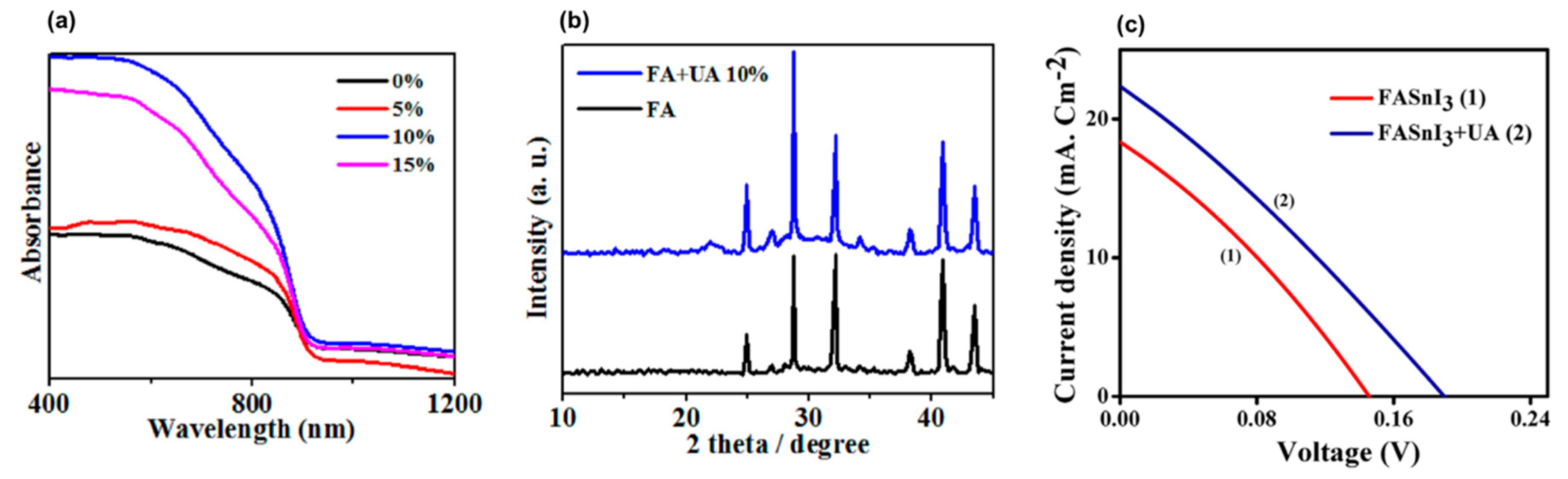
- Mohammadian-Sarcheshmeh, H.; Mazloum-Ardakani, M.; Rameez, M.; Shahbazi, S.; Diau, E.W.G. Application of a natural antioxidant as an efficient strategy to decrease the oxidation in Sn-based perovskites. J. Alloys Compd. 2020, 846, 156351. [Google Scholar] [CrossRef]
- Nagane, S.; Ogale, S. CH3NH3Pb(BF4)3 and (C4H9NH3)2Pb(BF4)4 Family of 3D and 2D Perovskites without and with Iodide and Bromide Ions Substitution. J. Phys. Chem. Lett. 2016, 7, 4757–4762. [Google Scholar] [CrossRef] [PubMed]
- Zhang, J.; Wu, S.; Liu, T.; Zhu, Z.; Jen, A.K.Y. Boosting Photovoltaic Performance for Lead Halide Perovskites Solar Cells with BF4− Anion Substitutions. Adv. Funct. Mater. 2019, 29, 1–8. [Google Scholar] [CrossRef]
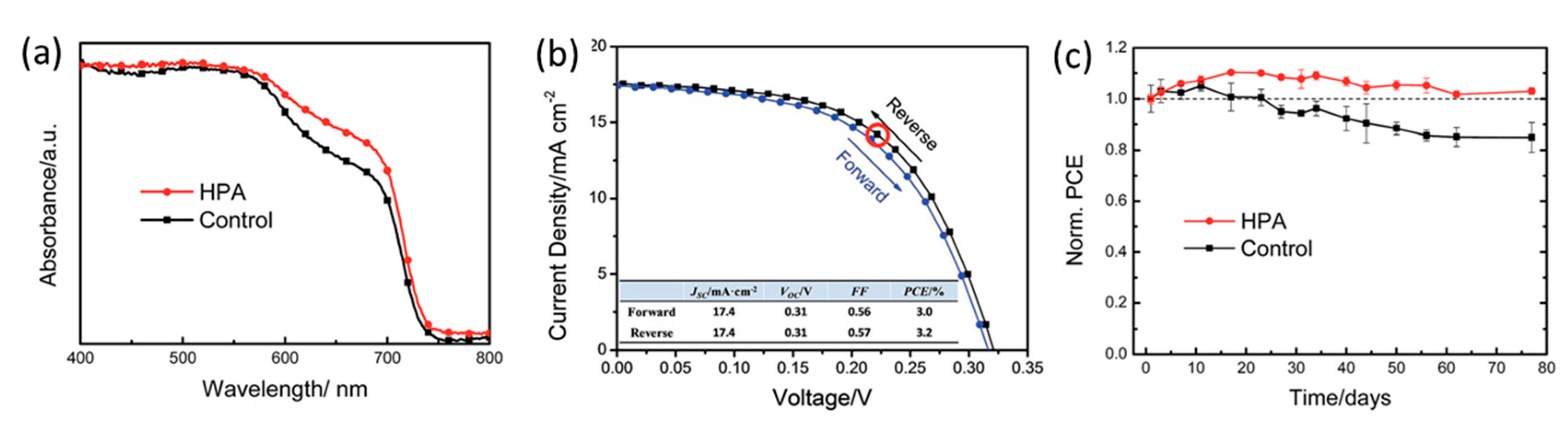
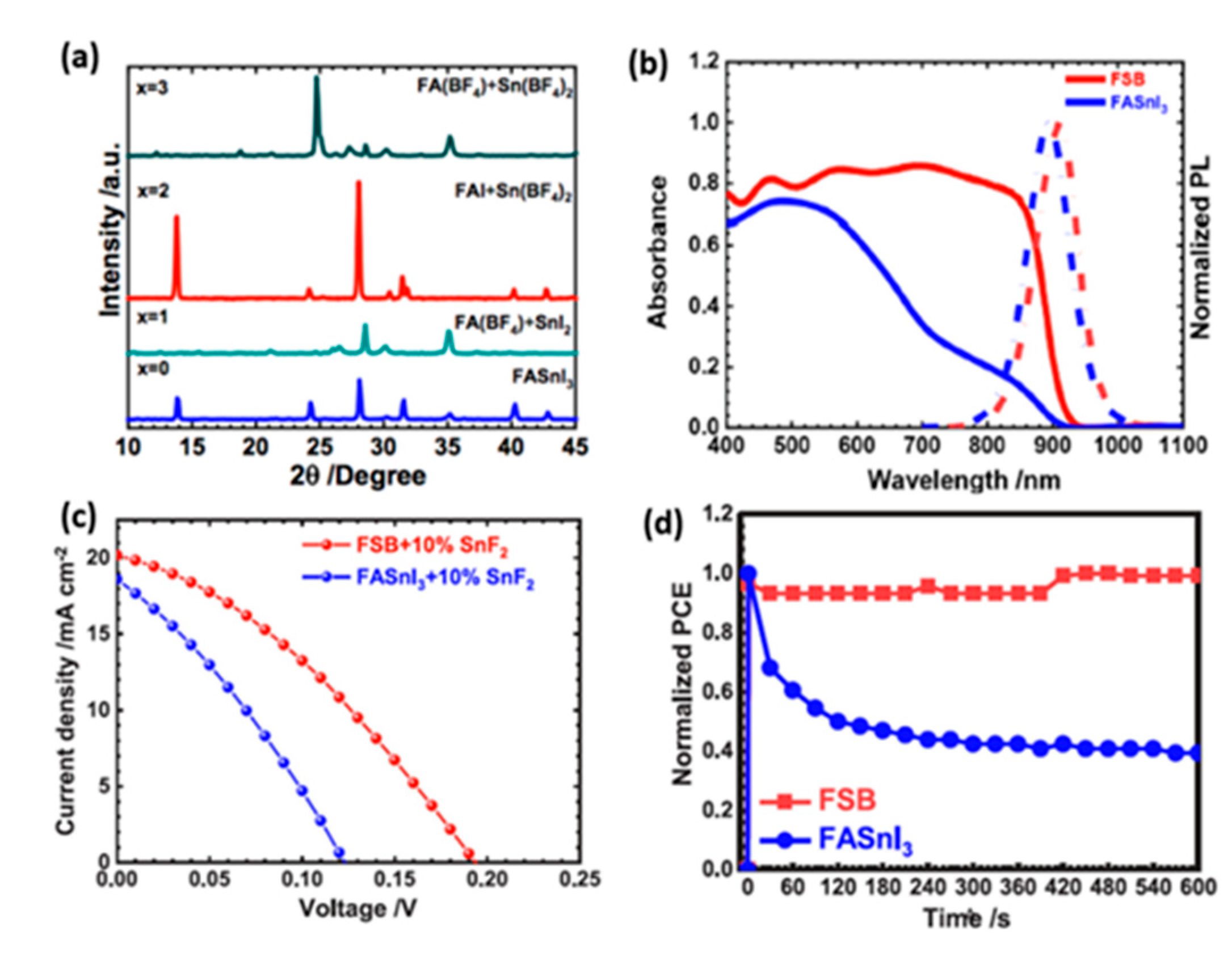
- Rameez, M.; Shahbazi, S.; Raghunath, P.; Lin, M.C.; Hung, C.H.; Diau, E.W.G. Development of Novel Mixed Halide/Superhalide Tin-Based Perovskites for Mesoscopic Carbon-Based Solar Cells. J. Phys. Chem. Lett. 2020, 11, 2443–2448. [Google Scholar] [CrossRef]
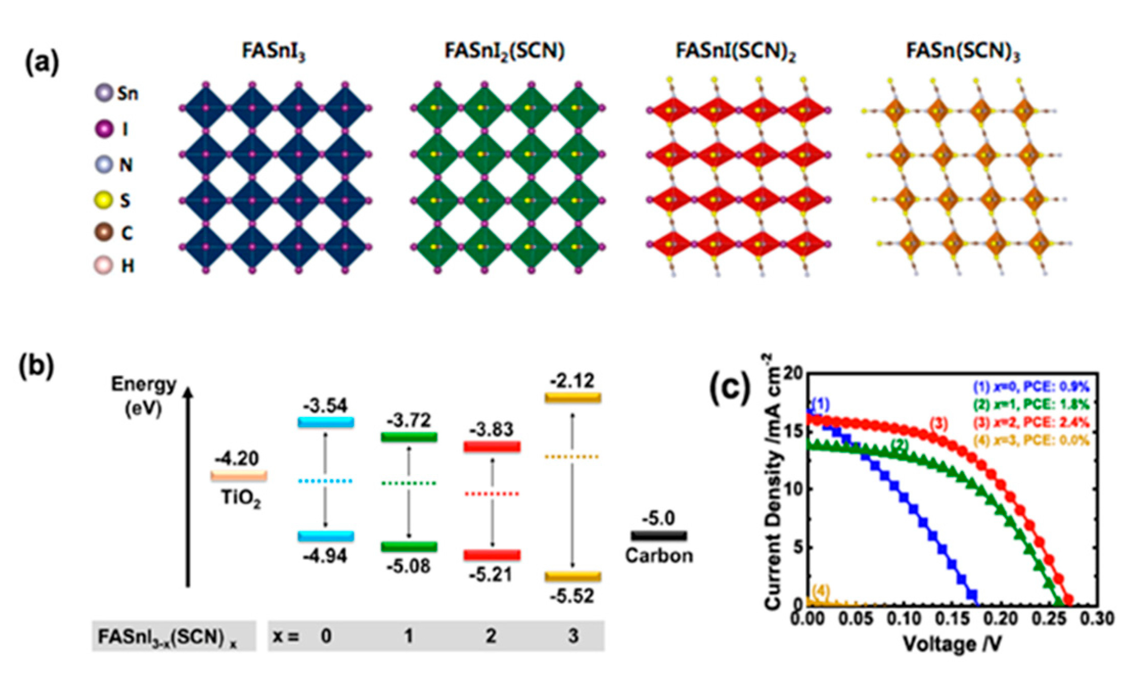
- Rameez, M.; Lin, E.Y.R.; Raghunath, P.; Narra, S.; Song, D.; Lin, M.C.; Hung, C.H.; Diau, E.W.G. Development of Hybrid Pseudohalide Tin Perovskites for Highly Stable Carbon-Electrode Solar Cells. ACS Appl. Mater. Interfaces 2020, 12, 21739–21747. [Google Scholar] [CrossRef]
- Smith, I.C.; Hoke, E.T.; Solis-Ibarra, D.; McGehee, M.D.; Karunadasa, H.I. A Layered Hybrid Perovskite Solar-Cell Absorber with Enhanced Moisture Stability. Angew. Chemie Int. Ed. 2014, 53, 11232–11235. [Google Scholar] [CrossRef]
- Yao, K.; Wang, X.; Xu, Y.X.; Li, F.; Zhou, L. Multilayered Perovskite Materials Based on Polymeric-Ammonium Cations for Stable Large-Area Solar Cell. Chem. Mater. 2016, 28, 3131–3138. [Google Scholar] [CrossRef]
- Tsai, C.M.; Lin, Y.P.; Pola, M.K.; Narra, S.; Jokar, E.; Yang, Y.W.; Diau, E.W.G. Control of Crystal Structures and Optical Properties with Hybrid Formamidinium and 2-Hydroxyethylammonium Cations for Mesoscopic Carbon-Electrode Tin-Based Perovskite Solar Cells. ACS Energy Lett. 2018, 3, 2077–2085. [Google Scholar] [CrossRef]
- Chen, M.; Ju, M.G.; Hu, M.; Dai, Z.; Hu, Y.; Rong, Y.; Han, H.; Zeng, X.C.; Zhou, Y.; Padture, N.P. Lead-Free Dion-Jacobson Tin Halide Perovskites for Photovoltaics. ACS Energy Lett. 2019, 4, 276–277. [Google Scholar] [CrossRef]
- Li, W.; Li, J.; Li, J.; Fan, J.; Mai, Y.; Wang, L. Addictive-assisted construction of all-inorganic CsSnIBr2 mesoscopic perovskite solar cells with superior thermal stability up to 473 K. J. Mater. Chem. A 2016, 4, 17104–17110. [Google Scholar] [CrossRef]
- Zhang, T.; Li, H.; Ban, H.; Sun, Q.; Shen, Y.; Wang, M. Efficient CsSnI3-based inorganic perovskite solar cells based on a mesoscopic metal oxide framework via incorporating a donor element. J. Mater. Chem. A 2020, 8, 4118–4124. [Google Scholar] [CrossRef]
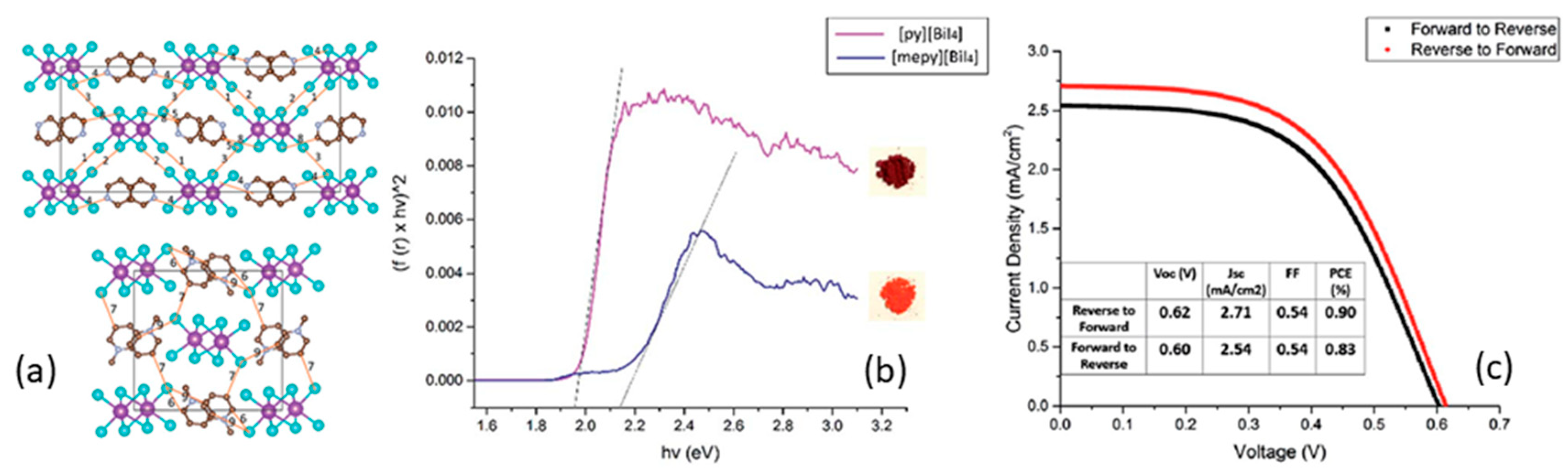
- Li, T.; Hu, Y.; Morrison, C.A.; Wu, W.; Han, H.; Robertson, N. Lead-free pseudo-three-dimensional organic-inorganic iodobismuthates for photovoltaic applications. Sustain. Energy Fuels 2017, 1, 308–316. [Google Scholar] [CrossRef] [Green Version]
- Li, T.; Wang, Q.; Nichol, G.S.; Morrison, C.A.; Han, H.; Hu, Y.; Robertson, N. Extending lead-free hybrid photovoltaic materials to new structures: Thiazolium, aminothiazolium and imidazolium iodobismuthates. Dalt. Trans. 2018, 47, 7050–7058. [Google Scholar] [CrossRef] [Green Version]
- Kong, M.; Hu, H.; Wan, L.; Chen, M.; Gan, Y.; Wang, J.; Chen, F.; Dong, B.; Eder, D.; Wang, S. Nontoxic (CH3NH3)3Bi2I9 perovskite solar cells free of hole conductors with an alternative architectural design and a solution-processable approach. RSC Adv. 2017, 7, 35549–35557. [Google Scholar] [CrossRef] [Green Version]
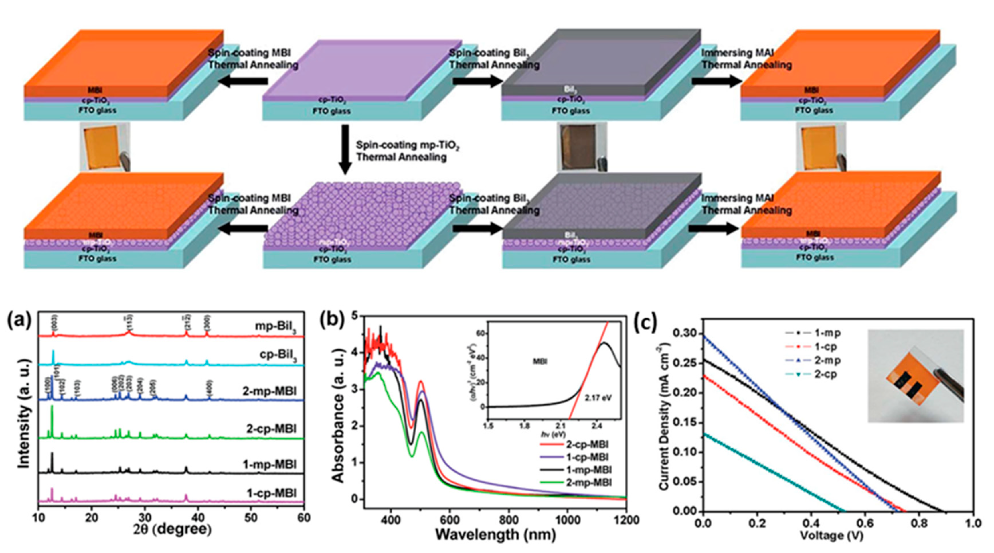
- Shin, J.; Kim, M.; Jung, S.; Kim, C.S.; Park, J.; Song, A.; Chung, K.B.; Jin, S.H.; Lee, J.H.; Song, M. Enhanced efficiency in lead-free bismuth iodide with post treatment based on a hole-conductor-free perovskite solar cell. Nano Res. 2018, 11, 6283–6293. [Google Scholar] [CrossRef]
- Jain, S.M.; Edvinsson, T.; Durrant, J.R. Green fabrication of stable lead-free bismuth based perovskite solar cells using a non-toxic solvent. Commun. Chem. 2019, 2, 1–7. [Google Scholar] [CrossRef] [Green Version]
- Li, J.; Duan, J.; Du, J.; Yang, X.; Wang, Y.; Yang, P.; Duan, Y.; Tang, Q. Alkali Metal Ion-Regulated Lead-free, All-Inorganic Double Perovskites for HTM-free, Carbon-Based Solar Cells. ACS Appl. Mater. Interfaces 2020, 12, 47408–47415. [Google Scholar] [CrossRef]
- He, F.; Wang, Q.; Zhu, W.; Chen, D.; Zhang, J.; Zhang, C.; Hao, Y. Carbon-based, all-inorganic, lead-free Ag2BiI5 rudorffite solar cells with high photovoltages. Solid State Electron. 2021, 176, 107950. [Google Scholar] [CrossRef]
- Roknuzzaman, M.; Alarco, J.A.; Wang, H.; Ostrikov, K. (Ken) Structural, electronic and optical properties of lead-free antimony-copper based hybrid double perovskites for photovoltaics and optoelectronics by first principles calculations. Comput. Mater. Sci. 2021, 186, 110009. [Google Scholar] [CrossRef]
- Xiang, S.; Li, W.; Wei, Y.; Liu, J.; Liu, H.; Zhu, L.; Chen, H. The synergistic effect of non-stoichiometry and Sb-doping on air-stable α-CsPbI3 for efficient carbon-based perovskite solar cells. Nanoscale 2018, 10, 9996–10004. [Google Scholar] [CrossRef]
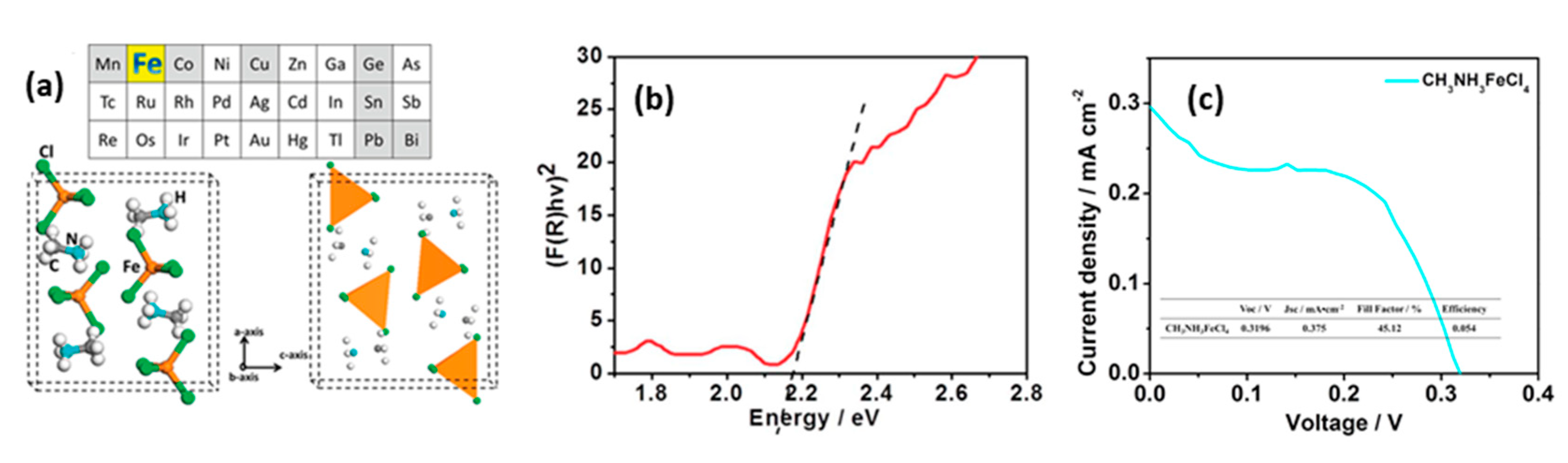
- Yin, J.; Shi, S.; Wei, J.; He, G.; Fan, L.; Guo, J.; Zhang, K.; Xu, W.; Yuan, C.; Wang, Y.; et al. Earth-abundant and environment friendly organic-inorganic hybrid tetrachloroferrate salt CH3NH3FeCl4: Structure, adsorption properties and photoelectric behavior. RSC Adv. 2018, 8, 19958–19963. [Google Scholar] [CrossRef] [Green Version]
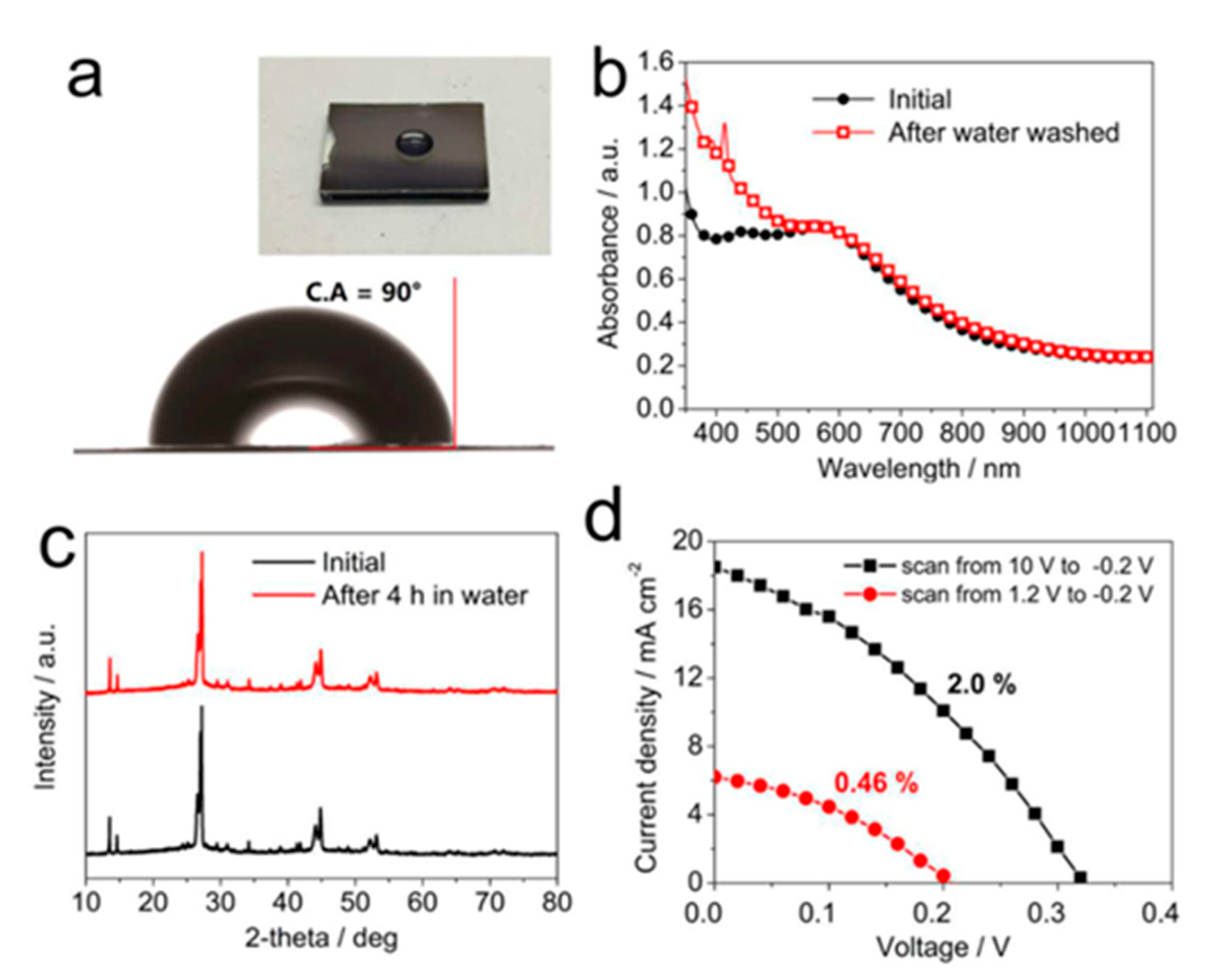
- Li, X.; Zhong, X.; Hu, Y.; Li, B.; Sheng, Y.; Zhang, Y.; Weng, C.; Feng, M.; Han, H.; Wang, J. Organic-Inorganic Copper(II)-Based Material: A Low-Toxic, Highly Stable Light Absorber for Photovoltaic Application. J. Phys. Chem. Lett. 2017, 8, 1804–1809. [Google Scholar] [CrossRef]
- Nie, Z.; Yin, J.; Zhou, H.; Chai, N.; Chen, B.; Zhang, Y.; Qu, K.; Shen, G.; Ma, H.; Li, Y.; et al. Layered and Pb-Free Organic-Inorganic Perovskite Materials for Ultraviolet Photoresponse: (010)-Oriented (CH3NH3)2MnCl4 Thin Film. ACS Appl. Mater. Interfaces 2016, 8, 28187–28193. [Google Scholar] [CrossRef] [PubMed]
- Schwartz, D.; Murshed, R.; Larson, H.; Usprung, B.; Soltanmohamad, S.; Pandey, R.; Barnard, E.S.; Rockett, A.; Hartmann, T.; Castelli, I.E.; et al. Air Stable, High-Efficiency, Pt-Based Halide Perovskite Solar Cells with Long Carrier Lifetimes. Phys. Status Solidi Rapid Res. Lett. 2020, 14, 1–8. [Google Scholar] [CrossRef]
- Tong, J.; Song, Z.; Kim, D.H.; Chen, X.; Chen, C.; Palmstrom, A.F.; Ndione, P.F.; Reese, M.O.; Dunfield, S.P.; Reid, O.G.; et al. Carrier lifetimes of >1 μs in Sn-Pb perovskites enable efficient all-perovskite tandem solar cells. Science 2019, 364, 475–479. [Google Scholar] [CrossRef]
- Wei, M.; Xiao, K.; Walters, G.; Lin, R.; Zhao, Y.; Saidaminov, M.I.; Todorović, P.; Johnston, A.; Huang, Z.; Chen, H.; et al. Combining Efficiency and Stability in Mixed Tin–Lead Perovskite Solar Cells by Capping Grains with an Ultrathin 2D Layer. Adv. Mater. 2020, 32, 1907058. [Google Scholar] [CrossRef] [PubMed]
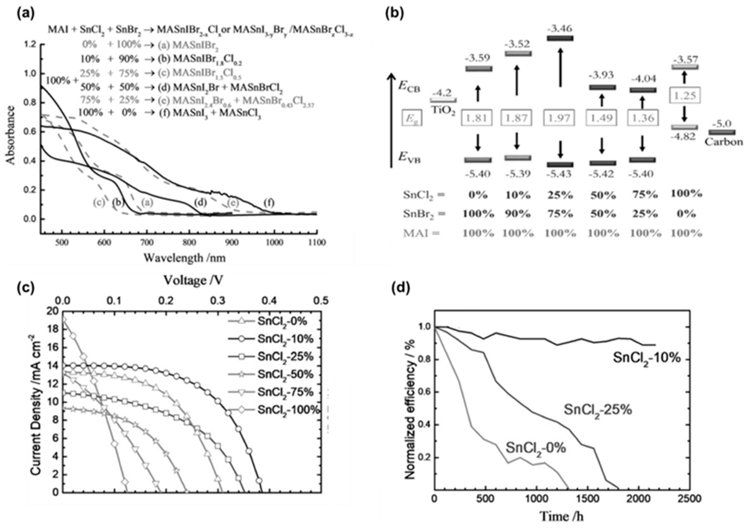
- Tsai, C.M.; Wu, H.P.; Chang, S.T.; Huang, C.F.; Wang, C.H.; Narra, S.; Yang, Y.W.; Wang, C.L.; Hung, C.H.; Diau, E.W.G. Role of Tin Chloride in Tin-Rich Mixed-Halide Perovskites Applied as Mesoscopic Solar Cells with a Carbon Counter Electrode. ACS Energy Lett. 2016, 1, 1086–1093. [Google Scholar] [CrossRef]
- Liang, J.; Zhao, P.; Wang, C.; Wang, Y.; Hu, Y.; Zhu, G.; Ma, L.; Liu, J.; Jin, Z. CsPb0.9Sn0.1IBr2 Based All-Inorganic Perovskite Solar Cells with Exceptional Efficiency and Stability. J. Am. Chem. Soc. 2017, 139, 14009–14012. [Google Scholar] [CrossRef]


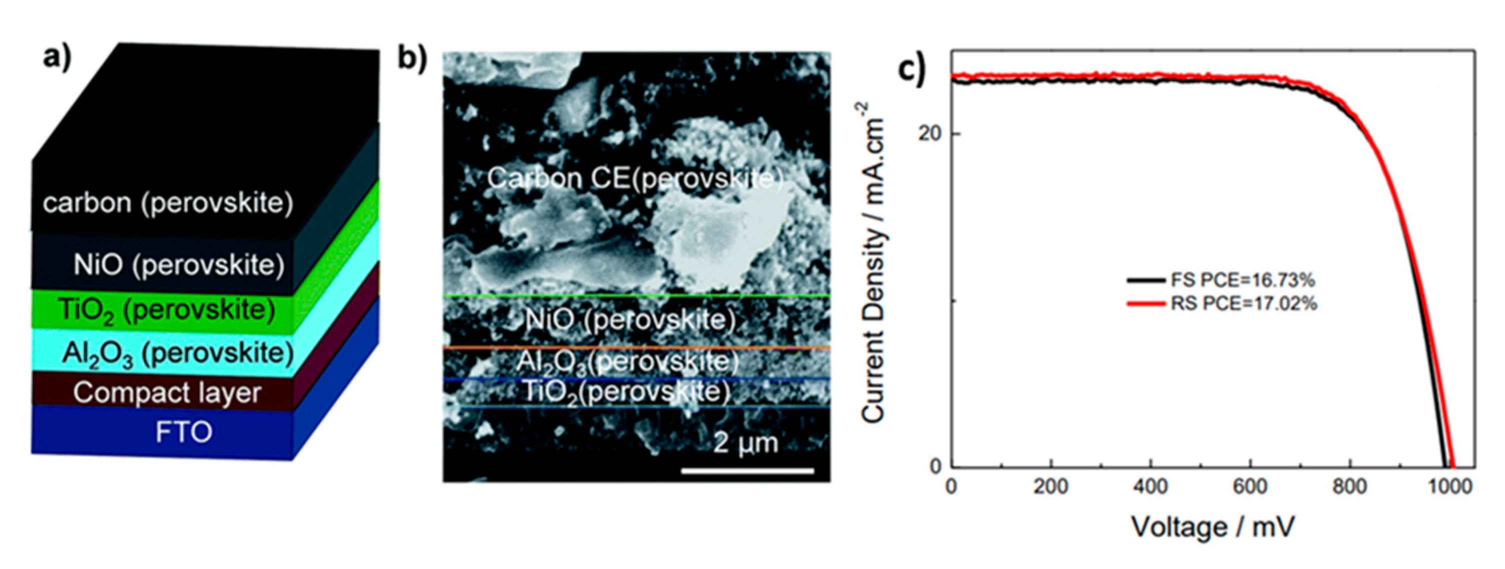
| PCE (%) | Perovskite | HTL | Device Configuration | Carbon Paste Formulation | Year/Reference | Comments |
|---|---|---|---|---|---|---|
| 17.02 | Cs0.05(FA0.4MA0.6)0.95PbI2.8Br0.2 | NiO | FTO/c-TiO2/mp-TiO2/Al2O3/NiO/C | Graphite/carbon black | 2017 [24] | sequential deposition |
| 16.51 | (5-AVA)x(MA)1−xPbI3 | - | FTO/c-TiO2/mp-TiO2/ZrO2/C | Commercial C paste | 2020 [25] | PBS-X; X = Li, Na, and K post treatment of TiO2/ZrO2/C |
| 16.37 | MAPbI3 | - | FTO/c-TiO2/mp-TiO2/PbTiO3/CNTs | CNTs sprayed | 2019 [23] | ultrathin layer of ferroelectric PbTiO3 on the TiO2 scaffold |
| 16.26 | Cs0.1Rb0.05FA0.85PbI3 | - | FTO/c-TiO2/mp-TiO2/ZrO2/ C | Carbon/spheroidal graphite | 2019 [26] | 1. DMF:DMSO: Formamide mixed solvent 2. Evaporation control |
| 15.9 | CH3NH3PbI3(SrCl2)x | - | FTO/c-TiO2/mp-TiO2/Al2O3/C | Graphite/ carbon black | 2016 [27] | SrCl2 chemical modification of perovskite |
| 15.77 | (5-AVA)x(MA)1−xPbI3 | - | FTO/c-TiO2/mp-TiO2/ZrO2/C | carbon black/graphite | 2019 [28] | VOx post-treatment of C/perovskite interface |
| 15.7 | (5-AVA)x(MA)(1−x)PbI3 | - | FTO/c-TiO2/mp-TiO2/ZrO2/C | Graphite/ carbon black | 2018 [29] | oxygen-rich carbon black |
| 15.6 | CH3NH3PbI3 | - | FTO/c-TiO2/mp-TiO2/ZrO2/C | Carbon/spheroidal graphite | 2017 [30] | 1.additive of ammonium chloride (NH4Cl) 2. Two-step process during perovskite formation |
| 15.6 | AB-MAPbI3 | - | FTO/c-TiO2/mp-TiO2/ZrO2/C | Graphite/ carbon black | 2017 [31] | 1. 4-(aminomethyl) benzoic acid hydroiodide (AB) organic cation 2. benzylamine hydroiodide (BA)benzylamine hydroiodide (BA) organic cation 3. 5-AVAI organic cation |
| 15.11 | (5-AVA)x(MA)1−xPbI3 | - | FTO/c-TiO2/mp-TiO2/ZrO2/C | Graphite/ carbon black | 2019 [32] | 1. Ethanol co-solvent in GBL |
| 15.03 | CH3NH3PbI3 | NiO | FTO/c-TiO2/mp-TiO2/Al2O3/NiO/C | Graphite/ carbon black | 2015 [33] | quadruple-layer architecture |
| 15 | CH3NH3PbI3 | - | FTO/c-TiO2/mp-TiO2/Al2O3/C | Graphite/ carbon black | 2017 [34] | 1. NMP solvent 2. slow crystallization (SC) method |
| 15 | Cs0.1FA0.9PbI3 | - | FTO/c-TiO2/mp-TiO2/ZrO2/C | Commercial C paste | 2019 [35] | Prepared in glove box |
| 14.9 | CH3NH3PbI3 | NiO | FTO/c-TiO2/mp-TiO2/ZrO2/NiO/C | Graphite/ carbon black | 2015 [36] | sequential deposition |
| 14.7 | CH3NH3PbI3 | - | FTO/c-TiO2/mp-TiO2/Al2O3/C | SWCNTs/carbon black | 2016 [22] | SWCNT-doped graphite/carbon black electrode |
| 14.5 | MAPbI3−xClx | - | FTO/c-TiO2/mp-TiO2/ZrO2/C | Carbon/spheroidal graphite | 2018 [37] | Addition of 0.45M MACl increases PCE from 8.74% to 14.5% |
| 14.5 | CH3NH3PbI3 | - | FTO/c-TiO2/mp-TiO2/ZrO2/C | N/A | 2016 [38] | Effect of LiCl additive |
| 14.3 | (5-AVA)x(MA) (1−x)PbI3 | - | FTO/c-TiO2/mp-TiO2/ZrO2/C | Commercial C paste | 2017 [39] | humidity assisted thermal exposure (HTE) as a post-treatment method—150 h |
| 14.27 | CH3NH3PbI3-xGuCl | - | FTO/c-TiO2/mp-TiO2/ZrO2/C | Commercial C paste | 2016 [40] | 1. Additive GuCl in perovskite 2. Voc 1.02V |
| 14.2 | CH3NH3I | NiO | FTO/c-TiO2/mp-TiO2/ZrO2/NiO/C | carbon black/graphite | 2015 [41] | 1. NiO nanosheet paste on ZrO2 2. Comparison of nanoparticles and nanosheets. 3. Screen printed device |
| PCE (%) | Perovskite | HTL | Device Configuration | Carbon Paste Formulation | Year/Reference | Comments |
|---|---|---|---|---|---|---|
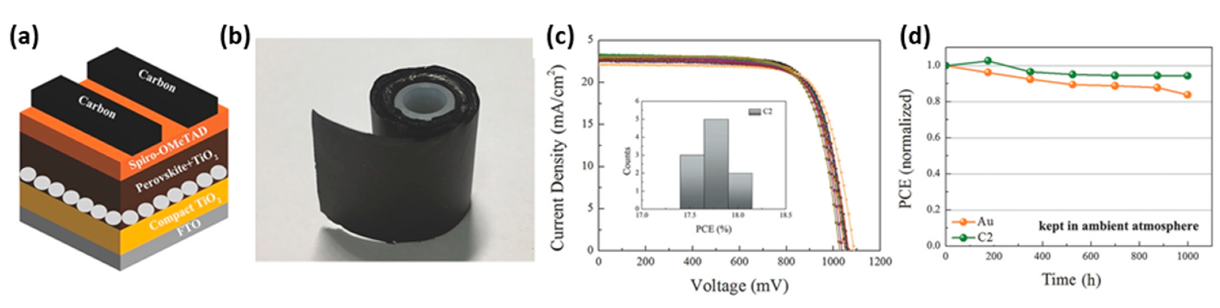
| 19.2 | (FA0.75MA0.25)PbI2.75Br0.25 | spiro-OMeTAD | FTO/c-TiO2/mp-TiO2/perovskite/spiro-OMeTAD/C | Commercial C paste | 2018 [44] | self-standing films |
| 18.65 | Cs0.05(MA0.17FA0.83)0.95Pb(I0.83Br0.17)3 | spiro-OMeTAD | FTO/c-TiO2/mp-TiO2/perovskite/spiro-OMeTAD/C | Graphene in IPA | 2019 [48] | various commercial carbon sources (carbon black, graphite sheet, and graphene) studied |
| 18.22 | FA0.3MA0.7PbI3 | P3HT/graphene | FTO/SnO2@TiO2/perovskite/P3HT/C | C in propylene glycol monomethyl ether acetate | 2019 [49] | Stability 89% of original PCE after 600 h |
| 18.1 | (FA0.83MA0.17)PbI2.15Br0.85 | CuSCN | FTO/c-TiO2/mp-TiO2/perovskite/CuSCN/C | graphitic carbon layer | 2019 [50] | ≈95% of their initial efficiencies for >2000 h under full-sun illumination |
| 17.78 | Cs0.05(MA0.17FA0.83)0.95Pb(I0.83Br0.17)3 | CuPc | FTO/Zn:SnO2/perovskite/CuPc/C | Commercial C paste | 2019 [51] | Zn-doped SnO2 ETL |
| 17.58 | Cs0.05(FA0.83MA0.17)0.95Pb(I0.83Br0.17)3 | CuSCN | FTO/c-TiO2/mp-TiO2/perovskite/CuSCN/C | MWCNTs in chlorobenzene | 2019 [52] | 1. MWCNTs to replace carbon black 2. Stability 80% after 1000 h 1 sun illumination |
| 17.56 | FACsPbI3 | spiro-OMeTAD | ITO/SnO2/perovskite/spiro-OMeTAD/C | free-standing CNT sheet | 2018 [46] | Trifluoromethanesulfonic acid vapor doping of the free-standing CNT sheet enabled tuning of conductivity and work function of electrode |
| 17.46 | Cs0.05(FA0.4 MA0.6)0.95PbI2.8Br0.2 | CuPc | FTO/Ni:TiO2/perovskite/CuPc/C | Commercial C paste | 2018 [53] | 1. planar 2. Ni-doped rutile TiO2 as electron transport layer |
| 17.02 | Cs0.05(FA0.85MA0.15)0.95Pb (I0.85Br0.15)3 | spiro-OMeTAD | FTO/SnO2/perovskite/spiro-OMeTAD/C | Self-adhesive carbon film | 2020 [45] | 1. planar 2.graphite paper/carbon film electrode |
| 16.6 | Cs0.05 (MA0.17FA0.83)0.95Pb(I0.83Br0.17)3 | spiro-OMeTAD | FTO/c-TiO2/m-TiO2/perovskite/C | SWCNT film | 2017 [54] | 1. press-transferred single-walled carbon nanotube (SWCNT) film infiltrated with Spiro-OMeTAD 2. superior long-term stability at elevated temperatures |
| 16.25 | FAxMA1−xPbIy Br3-y | - | ITO/SnO2/MWCNTs:perovskite/C | Commercial C paste | 2019 [55] | 1. MWCNTs additive in the perovskite solution 2. all air processed 3. stability 93% under ambient air conditions for 22 weeks |
| 16.2 | MAPbI3:MAPbIxBr3−x | - | FTO/c-TiO2/m-TiO2/perovskite/C | Commercial C paste | 2019 [56] | MAPbI3/MAPbIxBr3−x perovskite stacking structure |
| 16.1 | MAPbI3 | CuPc | FTO/c-TiO2/m-TiO2/perovskite/CuPc/Carbon | Commercial C paste | 2016 [57] | 8.5% drop during 600 h durability tests |
| 16.03 | MAPbI3 | - | ITO/HMB:C60/perovskite /C | Commercial C paste | 2019 [58] | 1. hexamethonium bromide-doped fullerene C60 ETL 2. No hysteresis |
| 15.73 | CH3NH3PbI3–SWCNT | - | FTO/c-TiO2/m-TiO2/perovskite/SWCNT–C | flaky graphite/spheroidal graphite/ carbon black | 2019 [59] | 1. SWCNTs in both anti-solvent and C electrode 2. stability of 90 days in dark under high humidity and high-temperature conditions |
| 15.6 | Cs0.05MA0.16FA0.79Pb(I0.84Br0.16)3 | - | FTO/c-TiO2/m-TiO2/perovskite/PEA2PbI4/C | Commercial C paste | 2018 [60] | 1. 2D perovskite interlayer 2. Stability 92% of initial PCE after 1000 h of exposure to ambient conditions |
| 15.38 | MAPbI3 | - | FTO/C60/perovskite/C | Commercial C paste | 2018 [61] | 1. First report on fullerene ETL 2. Additional replacement of FTO with graphene based TC electrode |
| 15.29 | Cs0.04(MA0.17FA0.83)0.96Pb(I0.83Br0.17)3 | spiro-OMeTAD | FTO/c-TiO2/m-TiO2/perovskite/C+spiro-OMeTAD | Commercial C paste | 2016 [62] | Carbon cloth embedded in C paste electrode |
| 15.27 | MAPbI3:MA1−xCsxPbI3 | - | FTO/c-TiO2/m-TiO2/perovskite/C | Graphite/carbon black | 2020 [63] | Post treatment with acetate salts (CsAc, FAAc, MAAc, KAc, NaAc) |
| 15.23 | MAPbI3 | - | FTO/c-TiO2/m-TiO2/m-Al2O3/perovskite/C | MWCNTs in chlorobenzene | 2017 [64] | Boron doping of MWCNTs for enhanced hole extraction |
Publisher’s Note: MDPI stays neutral with regard to jurisdictional claims in published maps and institutional affiliations. |
© 2021 by the authors. Licensee MDPI, Basel, Switzerland. This article is an open access article distributed under the terms and conditions of the Creative Commons Attribution (CC BY) license (https://creativecommons.org/licenses/by/4.0/).
Share and Cite
Bidikoudi, M.; Simal, C.; Stathatos, E. Low-Toxicity Perovskite Applications in Carbon Electrode Perovskite Solar Cells—A Review. Electronics 2021, 10, 1145. https://doi.org/10.3390/electronics10101145
Bidikoudi M, Simal C, Stathatos E. Low-Toxicity Perovskite Applications in Carbon Electrode Perovskite Solar Cells—A Review. Electronics. 2021; 10(10):1145. https://doi.org/10.3390/electronics10101145
Chicago/Turabian StyleBidikoudi, Maria, Carmen Simal, and Elias Stathatos. 2021. "Low-Toxicity Perovskite Applications in Carbon Electrode Perovskite Solar Cells—A Review" Electronics 10, no. 10: 1145. https://doi.org/10.3390/electronics10101145
APA StyleBidikoudi, M., Simal, C., & Stathatos, E. (2021). Low-Toxicity Perovskite Applications in Carbon Electrode Perovskite Solar Cells—A Review. Electronics, 10(10), 1145. https://doi.org/10.3390/electronics10101145