Article

An Analog Voltage Similarity Circuit with a Bell-Shaped Power Consumption

Department of Microsystems, University of South-Eastern Norway, 3679 Horten, Norway
*
Author to whom correspondence should be addressed.
Authors contributed equally to this work.
Electronics 2021, 10(10), 1141; https://doi.org/10.3390/electronics10101141
Submission received: 25 March 2021 / Revised: 25 April 2021 / Accepted: 30 April 2021 / Published: 11 May 2021
(This article belongs to the Section Circuit and Signal Processing)

Abstract

:
This paper presents a voltage similarity circuit (bump circuit) based on a novel voltage correlator. The proposed circuit is characterized by a power consumption which depends on the similarity between the two inputs. The sensitivity of the bump circuit and the power consumption are at the highest values when the inputs are equal. As the similarity between the input voltages decreases, the total current consumption decreases with a bell-shaped behavior. The proposed bump circuit is very simple in design, made of a new voltage correlator circuit in combination with a differential pair and mimics the behavior of the classical bump circuit. The voltage correlator was implemented using A M S 350 nm CMOS technology. Simulation and measurement results suggests that a low power consumption may be achieved if the circuit is used in applications where the input signals have large dissimilarity for most of the circuit operation.

1. Introduction

Circuits performing mathematical and logical operations, have been a research subject for many years [1]. Electrical signals, i.e., currents and voltages are suited for this purpose and variety of circuits and systems are proposed throughout the years. Circuits based on operational Amplifiers [2,3] can perform operations, such as addition, integration, inversion, multiplication, exponentiation, logarithm, division, etc. Analog signal processing, however, suffers from inaccuracy and is more susceptible to noise compared to their digital counterparts. Today, digital signal processing has become the dominant method thanks to introduction of integrated circuits which allows for higher integration and clock speeds. Despite this fact, analog signal processors are often far more effective and simpler in design than their digital counterparts [4,5,6]. Finding similarity or correlation between two or more analog signals is a good example. Current correlators [7] are used to find the correlation between two currents and voltage similarity circuits to find the similarity between voltages. One of the simplest and well-known voltage similarity circuits is the bump circuit presented by Tobias Delbrück [8] in 1991. Voltage similarity circuits are widely used in analog systems, such as in ultra low power energy harvesters [9], neuromorphic systems [10], and biological inspired circuits [11]. One of the main challenges with these circuits are the relatively high power consumption as they must be active all the time. Different approaches exist to lower the power consumption, such as clocking and/or lowering the power supplies, optimizing transistor sizes, and/or decreasing the bias voltages to limit the currents in the circuits. All of these methods will affect the operation of the circuit and can potentially decrease the sensitivity. Lu et al. [12] presented a bump circuit with a power consumption of 18.9 n W @ V d d = 3 V using a novel pseudo-differential transconductor. This circuit requires additional complicated biasing circuitry which may make the design more challenging compared to the presented circuit. Pheng et al. [13] exploit the properties of multiple input floating-gate technique to realizes a tunable bump circuit. The main drawback with this circuit is that it needs a complicated digital circuitry for programming the floating gates. Other similarity circuits have also been presented which offer tunability [14,15,16].
This paper is an extended version of a previously published paper [17], which introduced the concept. In that paper, we presented a new voltage similarity circuit (bump circuit) where the power consumption depends on the input voltages. It can potentially have lower power consumption compared to the classic bump circuit with the same functionality. In this paper, we present measurements results from a 350 nm ASIC from A M S and compare these to simulations. Simulations are done using Cadence with 350 nm CMOS models from AMS. In addition, the gain and common-mode behavior of the circuit are analyzed and an example of a energy harvester system, which may take advantage of the proposed bump circuit is presented.

2. New Voltage Correlator Circuit

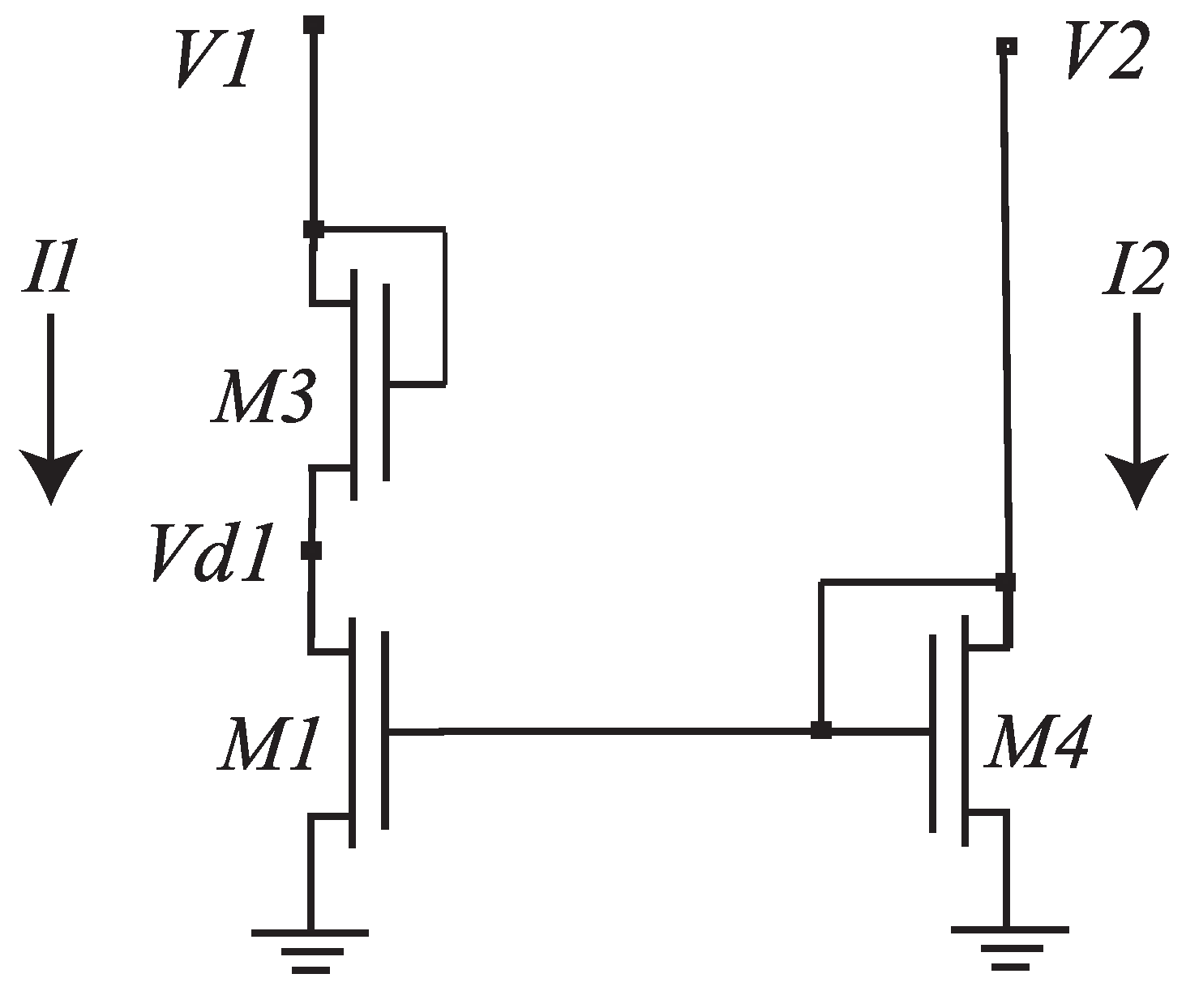
The proposed voltage correlator circuit is shown in Figure 1. The correlator circuit consists of two equal legs with diode-connected transistors M 3 and M 4 in series with transistors M 1 and M 2 , respectively. The gates of transistors M 1 and M 2 are connected to the gate of diode-connected transistor at the opposite leg. If the voltages V 1 and V 2 are equal and high enough to keep M 1 and M 2 in triode, i.e., V g s 1 , 2 > V t h + V d 1 , 2 , both legs conduct equally, and the currents are at their maximum values.
In this state, the currents I 1 and I 2 are roughly decided by the diode-connected transistors that are in saturation and can be approximated by
I 1 , ( 2 ) = β 3 , ( 4 ) 2 ( V 1 V d 1 , ( d 2 ) V t h ) 2 ,
where β = μ C o x ( W / L ) , and V t h is the threshold voltage. Assuming M 1 and M 2 are in deep triode, V d 1 and V d 2 can be given as
V d 1 , ( d 2 ) = I 1 , ( 2 ) × R M 1 , ( 2 ) = I 1 , ( 2 ) β 1 , ( 2 ) ( V 1 ( 2 ) V t h )
where R M 1 , 2 are the channel resistances at deep triode, which may be approximated by
R M 1 , ( 2 ) = 1 β 2 , ( 1 ) × ( V 2 , ( 1 ) V t h ) .
As the voltages V 1 and V 2 across the two legs become different, the transistors will behave differently. If all the transistors in the circuit are equal in size, currents in both legs will remain almost equal. In this state, the currents are always limited by the leg with the lowest of the two voltages. If V 1 increases and V 2 decreases, the voltages across M 1 and M 3 increase, and M 1 goes into saturation, and M 2 goes into deeper triode region. According to Equation (3), the resistance of M 2 decreases, and the voltage V d 2 approaches the ground value. In this state, M 4 forms a current mirror with M 1 , which controls and limits the current I 1 equal to I 2 , as shown in Figure 2. The body effect of M 4 decreases as its source approaches ground. Similar behavior can be expected when V 2 becomes larger than V 1 .
As V 2 decreases, I 1 will decrease. If we ignore the channel modulation effect of M 1 , the current I 1 can be expressed as:
I 1 = I 2 = β 4 2 ( V 2 V t h ) 2 .
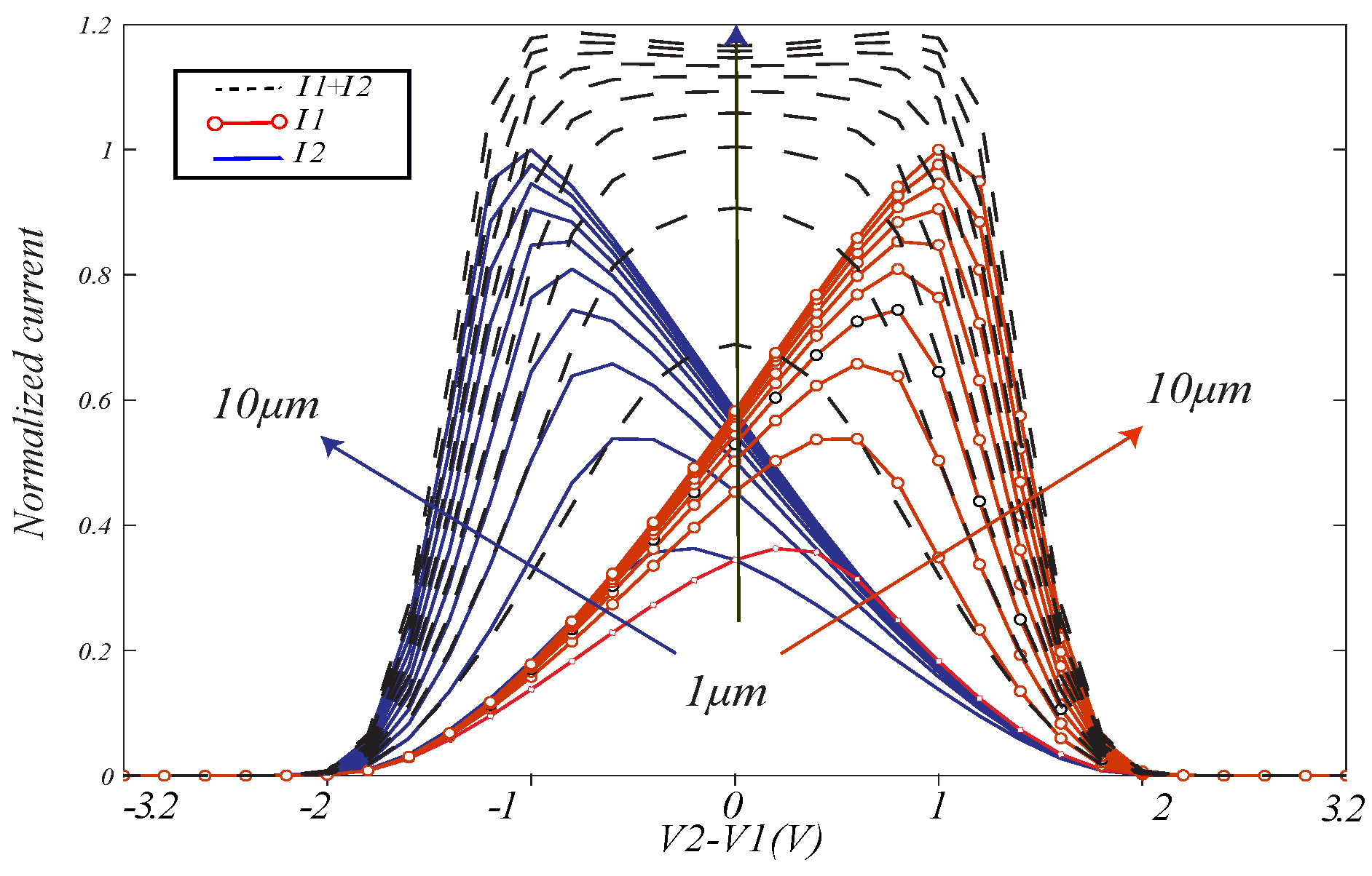
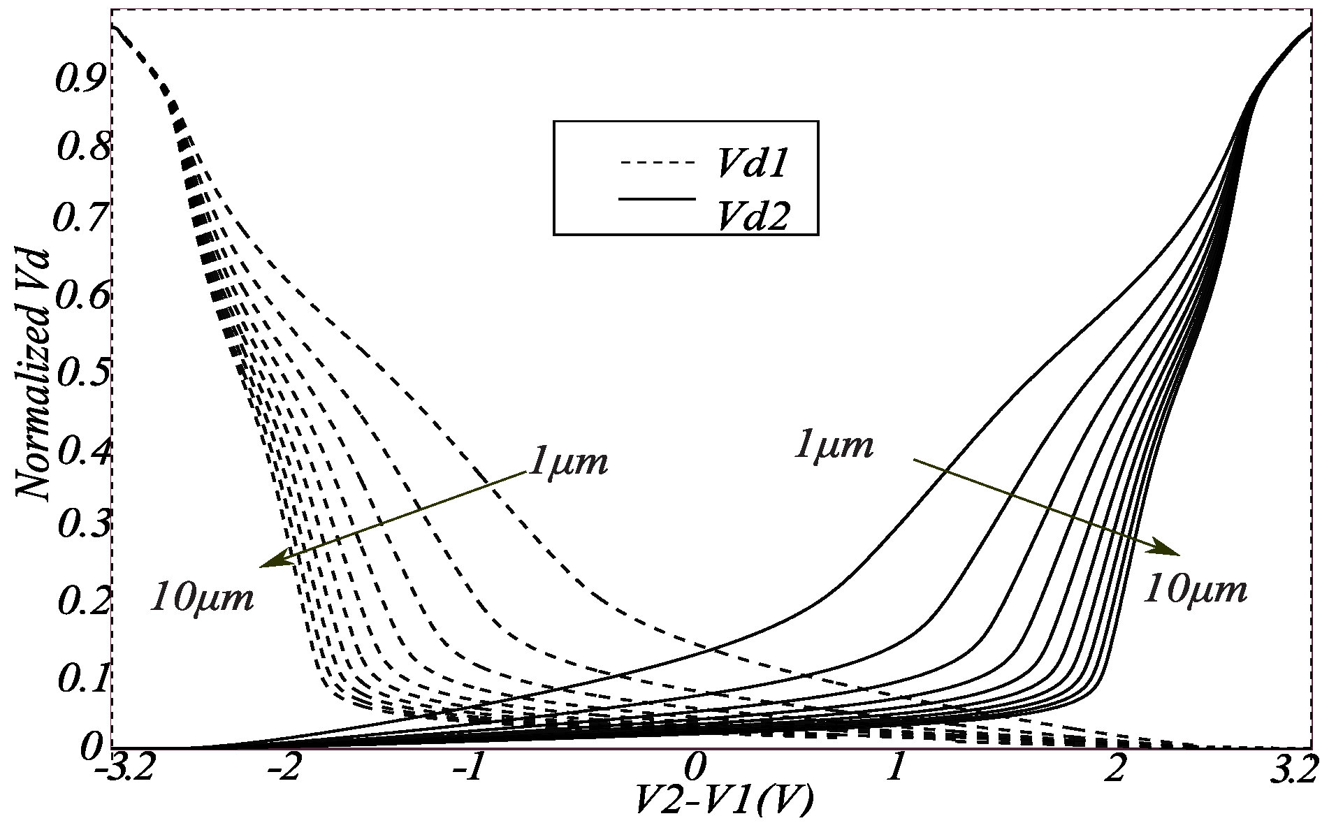
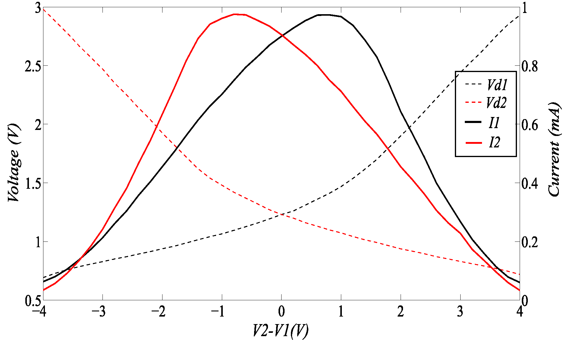
As explained earlier, the correlation between the two voltages V 1 and V 2 is through the current mirrors created between the two legs of circuit. The weighting between the transistors forming the current mirror will, therefore, control the amount of current in each leg. Figure 3 and Figure 4 show how the voltages V d 1 , V d 2 and the currents I 1 and I 2 are affected when the widths of the transistors M 1 and M 2 are increased from 1 μ m to 10 μ m simultaneously, and M 3 and M 4 are kept constant at 1 μ m. From the current simulation in Figure 3, we can see that the two currents are equal and at their maximum when V 1 is approximately equal to V 2 when all device widths are 1 μ m, i.e., the mirror is balanced. This figure shows that as the widths increase, the currents increase. When the mirror is formed due to difference between the voltages V 1 and V 2 , the increased width increases the difference between the currents. Figure 4 shows as the widths increase, the voltages V d 1 and V d 2 are pulled closer to ground due to even larger ratio between the transistors in the current mirrors and higher conductivity in the transistors, i.e., less resistance. To summarize, the increased width has two important effects, one is that the resistance of the transistor in triode decreases, which makes the current mirror more ideal with less body effect and it makes the mirror unbalanced, i.e., the current in one leg becomes higher than the other one. As we will show later when this circuit is used in a bump circuit, an unbalanced current mirror is necessary to create the bump at the output current correlator.
The transistors in the simulations and measurements presented have lengths of 500 nm and widths of 1 μ m if not stated in the text explicitly. Transistors M1 and M2 have widths of 15 μ m. The bias voltage V B i a s is set to 2.35 V, and V d d is 3.2 V in both measurements and simulations if not stated explicitly in the text.

Voltage Correlator Connected to a Differential Pair

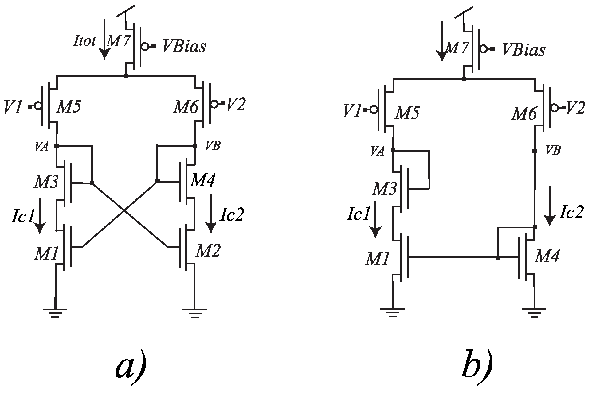
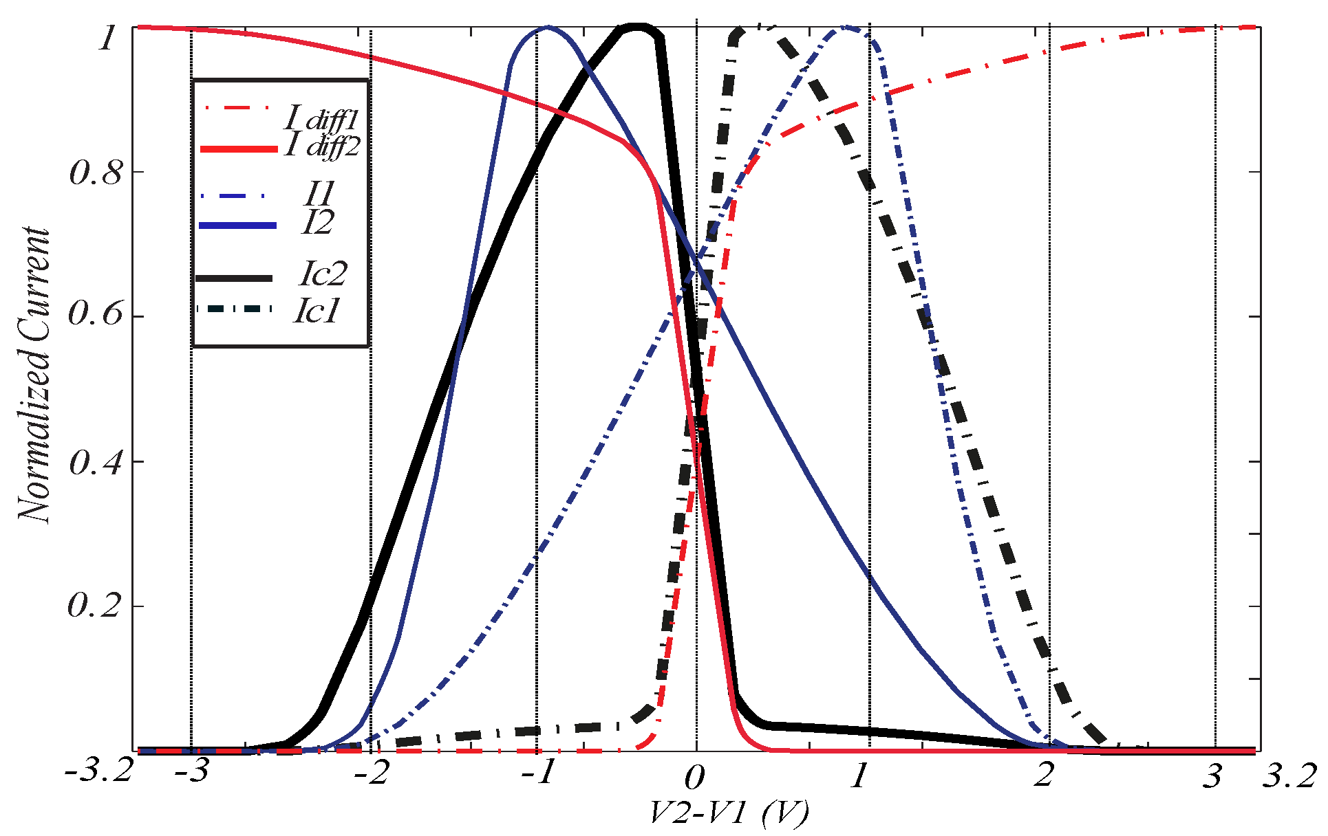
By cascoding a PMOS differential pair to the voltage correlator as shown in Figure 5a, the functionality of these two circuits is combined. The currents through each leg of the combined circuit are denoted I c 1 and I c 2 and shown in Figure 6 as the black curves. This figure shows also the currents in the voltage correlator I 1 , I 2 presented earlier as the blue curves and the currents in a different pair denoted I d i f f 1 , I d i f f 2 as the red curves for comparison. The solid curves are the currents through the left leg, and the dashed ones are the currents in the right leg. The rapid decrease of current when the two inputs become equal is caused by the differential pair. From the simulation, we can see that currents I c 1 , I c 2 follow I d i f f 1 , I d i f f 2 when the two input voltages are close to each other and follow the currents I 1 , I 2 when the inputs become different.
When the inputs are equal, the transistors M 1 and M 2 are in deep triode and all other transistors are in saturation, i.e., voltages V A and V B will be just above threshold voltage. The current can be approximated as
I c 1 = I c 2 = β 6 ( 5 ) 2 ( V d d V 2 ( 1 ) V t h ) 2 .
As the difference between the inputs increases, the circuit will change its state. Assuming V 1 decreases and V 2 increases, the circuit can be represented as in Figure 5b. Transistors M 5 and M 2 go into triode and all the others in saturation. The current I c 2 is then mirrored into I c 1 . M 3 will act as a diode connected transistor with a voltage approximately equal to the threshold voltage across it. The current in this state can be approximated as
I c 1 = I M 1 = I M 3 = I M 5 = K I M 6 ,
where K is the ratio between the widths of the transistors forming the mirror M 1 and M 4 . If we ignore the effect of this diode connected transistor, i.e. M 3 , and assuming that M5 is in deep triode, the circuit can be modeled in strong inversion as
I c 1 = β 5 ( ( V d d V 1 V t h ) V D S ) = K β 6 2 ( V d d V 2 V t h ) 2 .
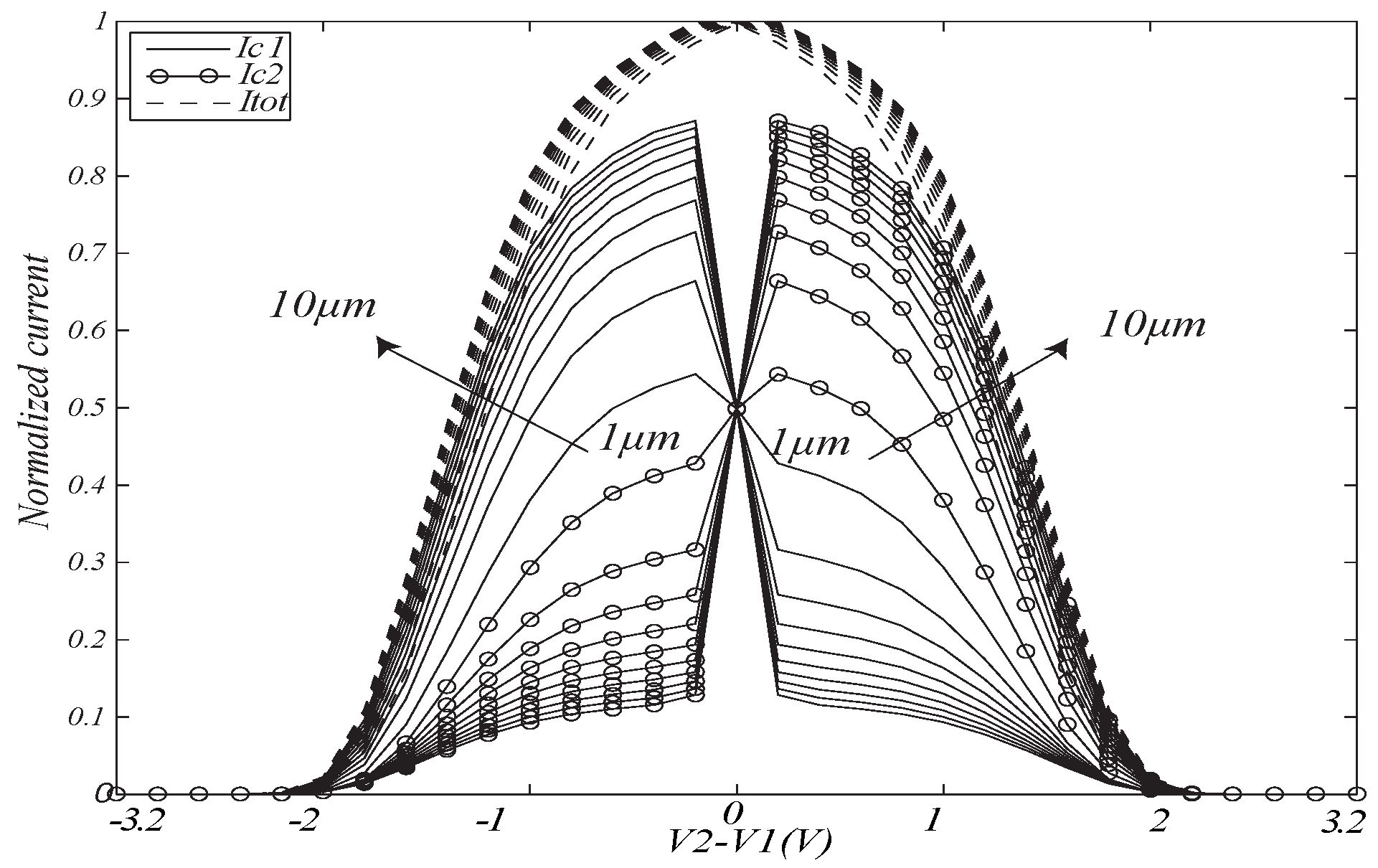
Figure 7 shows the currents in circuit shown in Figure 5a when the widths of transistors M 1 and M 2 are increased from 1 μ m to 10 μ m simultaneously, and M 3 and M 4 are kept constant at 1 μ m. From the figure, we can see that the variations in currents due to the changes in the width of the transistors are smaller compared to the simulation in Figure 3, which is caused by the differential pair. The simulation shows the current I c 1 and I c 2 as solid and circled curves, respectively, and the total current in the circuit I t o t as dashed curves.

3. The Proposed Bump Circuit

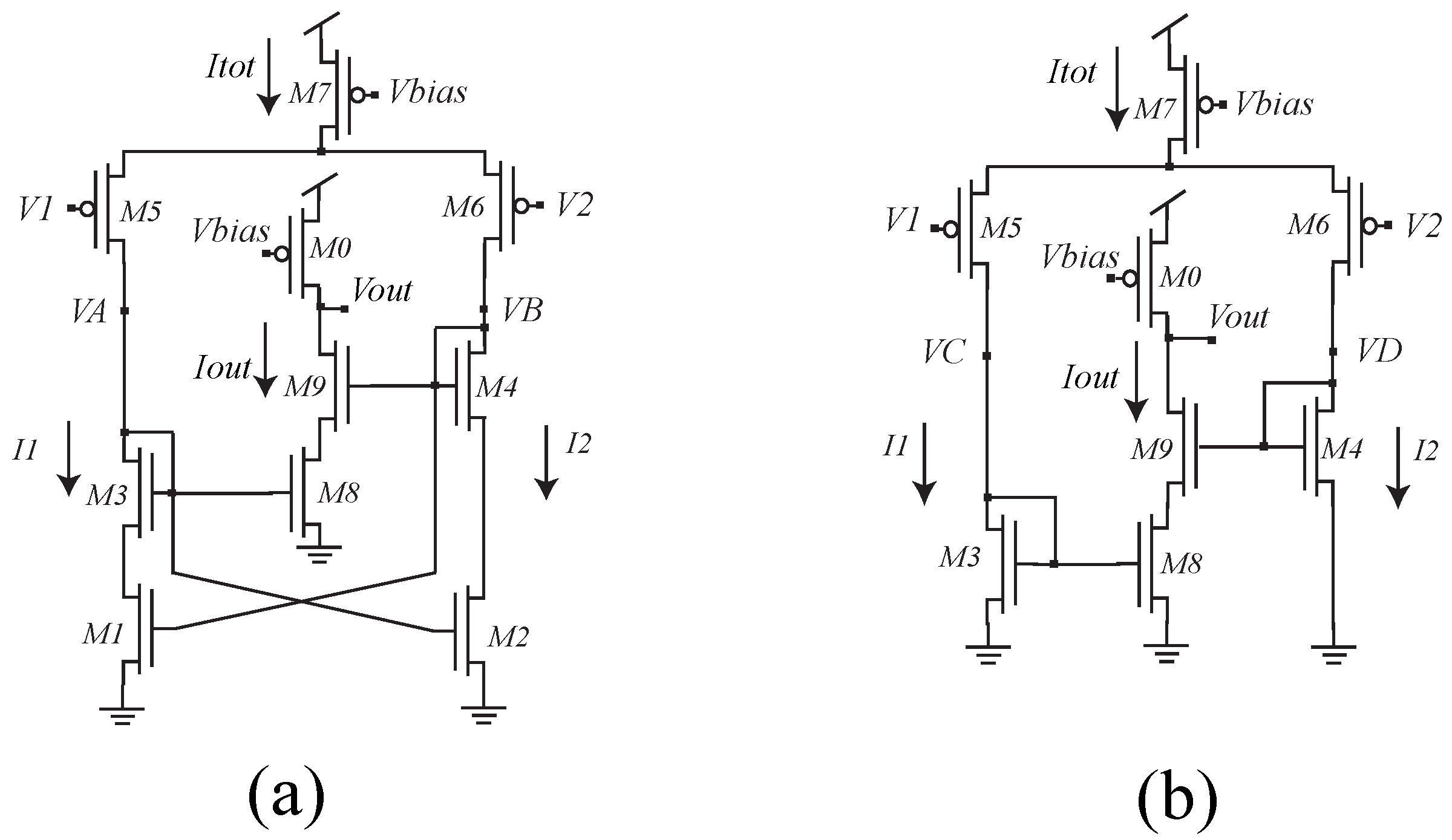
By correlating the currents I C 1 and I C 2 in the circuit shown in Figure 5a using a current correlator made of two series connected transistors, the circuit will become a voltage similarity (bump) circuit as shown in Figure 8a. This bump circuit will have a similar behavior as the classic bump circuit developed by Delbrück [8] shown in Figure 8b. The output current of the bump circuit in weak inversion and strong inversion are given in References [8,15], respectively.
When the inputs are similar, the circuits in Figure 8a,b will behave similar and have the same current consumption. When the inputs become different, the current consumption of the classic bump circuit increases, while the proposed bump circuit will have a decreasing power consumption.
Figure 9 shows the voltages at the drain of the different pair for both bump circuits denoted V A and V B in Figure 8a and V C and V D for the classic bump circuit in the Figure 8b. Voltages VA and VB in the proposed bump circuit change their state from rail to rail as the input voltages cross each other, but V C and V D in the classic bump circuit change only between ground and the threshold voltage of the devices as they are connected as diodes. Voltages V A and V B can in some cases be regarded as a digital signal that changes its state when the inputs cross each other.
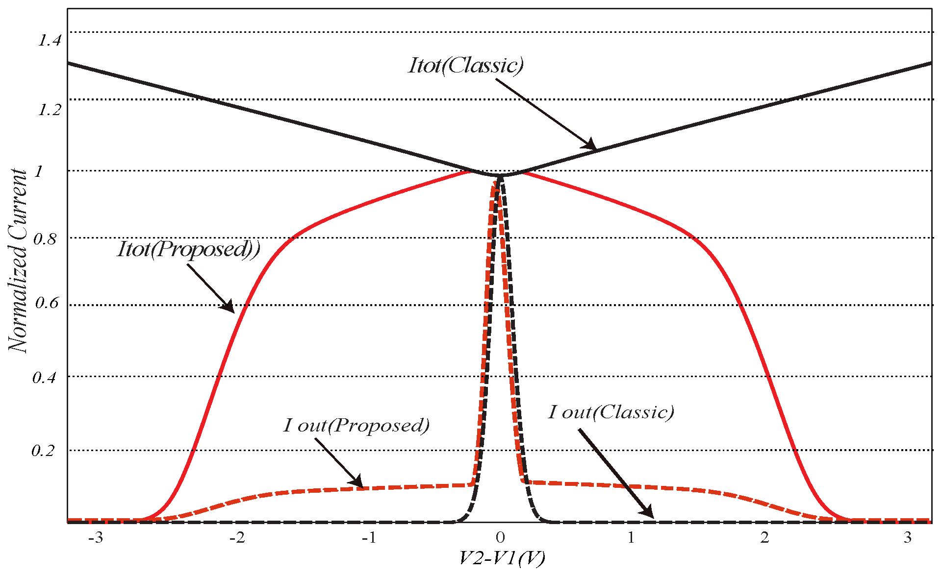
Figure 10 shows the simulation of the proposed bump circuit and the classic one when a differential voltage is applied to their inputs. The solid black and red colored curves marked I t o t are the total current consumption of the classic bump circuit and the new proposed circuit, respectively. The variation in current consumption of the proposed bump circuit follows a bell-shaped curve.
The total static power consumption for all the combination of the input voltages of the proposed bump circuit and the classic bump is illustrated as a 3-d graph in Figure 11a,b, respectively. It is clear from the simulation that the proposed bump circuit will achieve low power consumption when one or both of the inputs are close to V d d , approximately above 2.5 volts in this simulation.
The power consumed by the proposed bump circuit and the classic are compared and shown in Figure 11c. The relation between power of the two circuits increases exponentially with the increase in the difference between the input voltages. For the simulation in Figure 11c, it is as high as 5 orders of magnitude when the difference between the inputs approaches maximum.
The simulation in Figure 10 shows also the output currents I o u t in both the classic bump circuit as dashed black curve and the proposed bump circuit as dashed red curve. When the input voltages V 1 and V 2 are equal, I o u t is large and equal for both circuits. When the difference between the input increases, the output currents in both bump circuits decrease. In the classic bump circuit, the output current I o u t is close to zero as the inputs become different, while in the proposed bump circuit, the output current becomes null only when the | V 2 V 1 | 0 . This difference is due to the fact that the sources of the diode connected transistors M 3 and M 4 in the proposed circuit are not completely grounded when the inputs are different, causing the output transistors to leak. This current leakage can be reduced by increasing the width of the transistors M 1 and M 2 to create a stronger ground as explained in Section 2. The effect of increasing the width of these transistors are shown in Figure 3, Figure 4, and Figure 7.
A well known non-ideality of the current correlator used in both circuits is the asymmetric bump at the output, which is caused by the fact that the series connected transistors M 8 and M 9 have different source voltages. This can be solved by adding an extra pair of transistors connected in parallel with M 8 and M 9 where their gate connections are interchanged as in References [12,14].

Common-Mode Behavior of Proposed Bump Circuit

The behavior of the proposed bump circuit, including its power consumption and the gain, is highly dependent on the input common-mode voltage. Figure 12 shows the sensitivity (S) of the proposed bump circuit at different common-mode voltages defined as
S = d ( I 2 I 1 ) d ( V 2 V 1 ) .
The simulation results show that maximum gain is achieved at low common-mode voltages and decreases as the common mode voltage increases. This is expected due to larger currents in the circuit. This behavior would be opposite for NMOS input transistors, i.e., the gain would be at its maximum at higher voltages closer to Vdd.
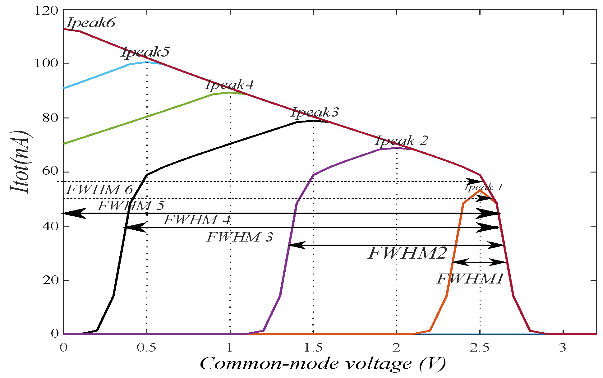
Figure 13 shows the power consumption of the proposed bump circuit at different input common-mode voltages. The figure shows the simulation when the inputs cross each other at common-mode voltage levels = 0 V, 0.5 V, 1 V, 1.5 V, 2 V, 2.5 V, and 3 V. This simulation shows that the power consumption increases as the similarity occurs at lower voltages. The change in the common-mode voltage also changes the width of the bell. To be able to analyze this characteristic in more details, we measured the full width of half the maximum ( F W H M ) of the bell-shaped current consumption as shown in Figure 13. We used two different parameters to analyze the power consumption as function of the common-mode voltage, quality Q and efficiency E. Q is the blue dashed curve in Figure 14 and defined as
Q = C M V F W H M
where C M V is the common-mode voltage. The power efficiency is shown as the green curve and defined as
E = I p e a k F W H M
where I p e a k is the maximum current consumption at the common-mode voltage and is shown in the figure as the black solid curve. The analysis show that efficiency reaches its maximum at common-mode voltage = 2.6 V. The product of the I p e a k and the F W H M is also shown as the dashed black curve which relates to the average power consumption. From these analyses, we can conclude that the circuit is more effective at common-mode voltages close to Vdd.
Table 1 compares the performance of the proposed circuit with other bump circuits described in the current literature.
The main feature and novelty of the presented circuit is that power consumption is dependent on the input voltages. To our knowledge, no other circuit offers this feature. Furthermore, it is worth mentioning that the design presented in this work was not optimized for minimum power consumption; however, we have achieve power consumption in nano-watt region. As the power consumption may vary and is dependent on application, we have chosen to compare the static power consumption when inputs are equal, i.e., maximum power consumption at common-mode voltage at Vdd/2.
The power consumption of Reference [8] is similar with ours as shown in the table. This is because the circuit in Reference [8] is most similar to ours and the best one for comparison. We have simulated both circuits and presented the results in Figure 10 and Figure 11. Table 1 shows the maximum power consumption of our circuit which decreases as the inputs become different as shown in Figure 11a, but, for Reference [8], the power increases as shown in Figure 10 and Figure 11b. The minimum power consumption of our circuit is not easy to determine as it can approach 0 and lower than Reference [12] when the difference between the inputs becomes large enough.

4. Measurement Results

The proposed bump circuit was fabricated using 350 nm CMOS from A M S . Micrograph of the bump circuit including two buffers used at the outputs is shown in Figure 15a. In this implementation, the bump was given a separate power supply pad in order to measure the characteristic bell shaped power consumption of the circuit. The output buffers are connected to V o u t and node V A . V B was omitted due to its symmetrical behavior. In the figure, all the circuit ports and some of the parts are marked with black text. In this chip, the transistors M 1 and M 2 have a width of 15 μ m and all others a width of 1 μ m.
The chip was mounted on chip-carrier and bonded in-house as shown in Figure 15b. Keysight DSOX3024T oscilloscope was used to read the output values, Fluke 45 multimeters was used for current measurement and Agilent 33521A signal generators was used to generate the input signals. The system was powered using GW GPS-3030 power supply. Figure 16 shows the measurement of the output voltage V o u t and the node V A at 10 kHz frequency. The behavior of the circuit matches the simulation result shown in Figure 9, which is shown as the black dashed curve in the figure. The node V A (red curve) follows V 2 and is at its lowest value when the input V 2 is at its minimum value. The voltage V o u t goes low when the inputs are equal. V o u t does not reach ground. The reason for this is unknown, but we think it may be due to the type of pad we used, which doesn’t have the correct ground value since the chip was a mixed design sharing pads with other circuitry.
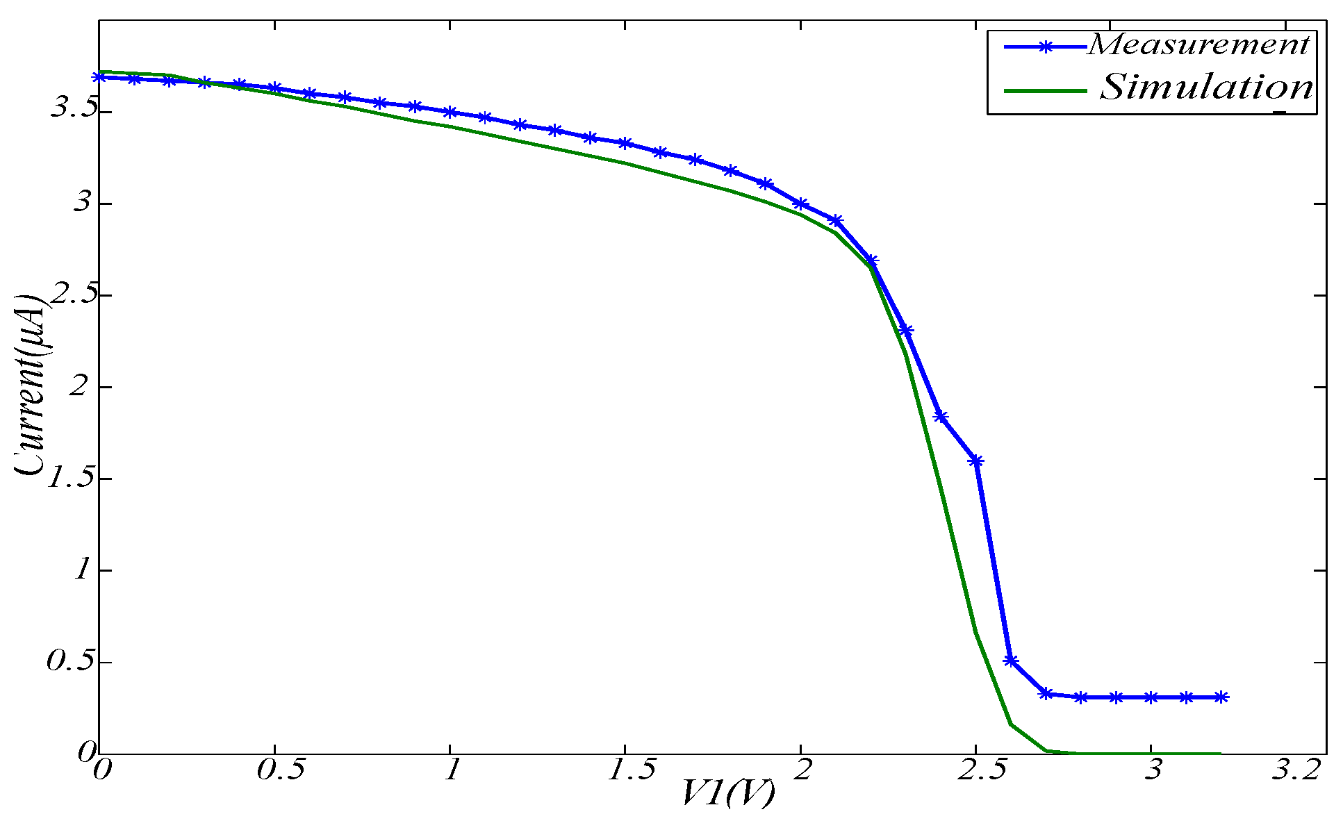
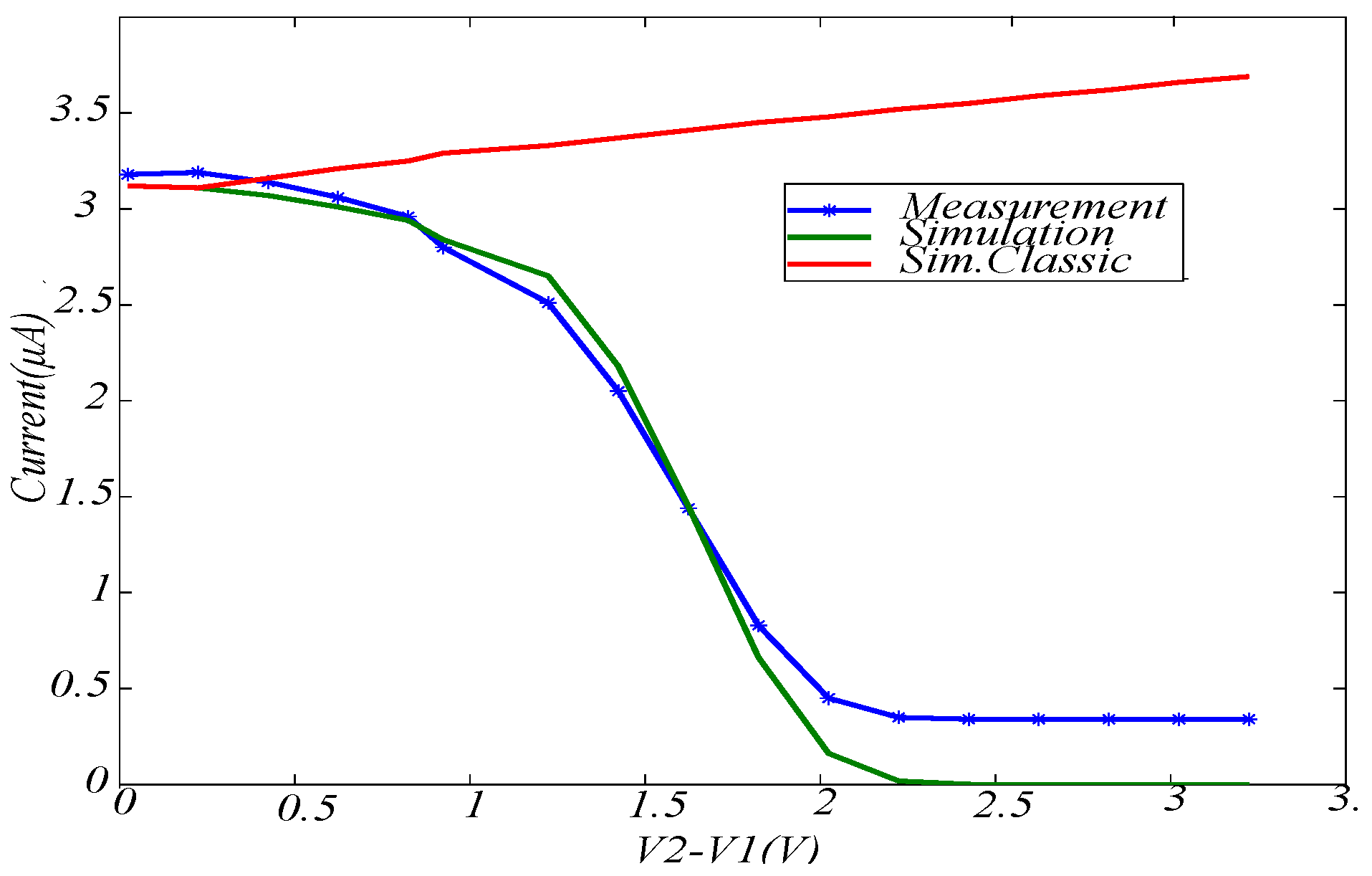
Figure 17 shows the measured power consumption of the proposed bump circuit when V 2 is grounded, and V 1 is increased from ground to V d d . The blue curve is the measurement result, and the green is the simulation result. The measured current does not reach zero due to the leakages in the protection diodes in the pad. Figure 18 shows the power consumption when the V 1 is decreased to ground from V d d / 2 and V 2 increased from V d d / 2 to V d d simultaneous. In this figure, we have also added the simulation result for the classic bump circuit for comparison. The two previous measurement result confirm the variation in the power consumption of the circuit as a function of the input voltages.
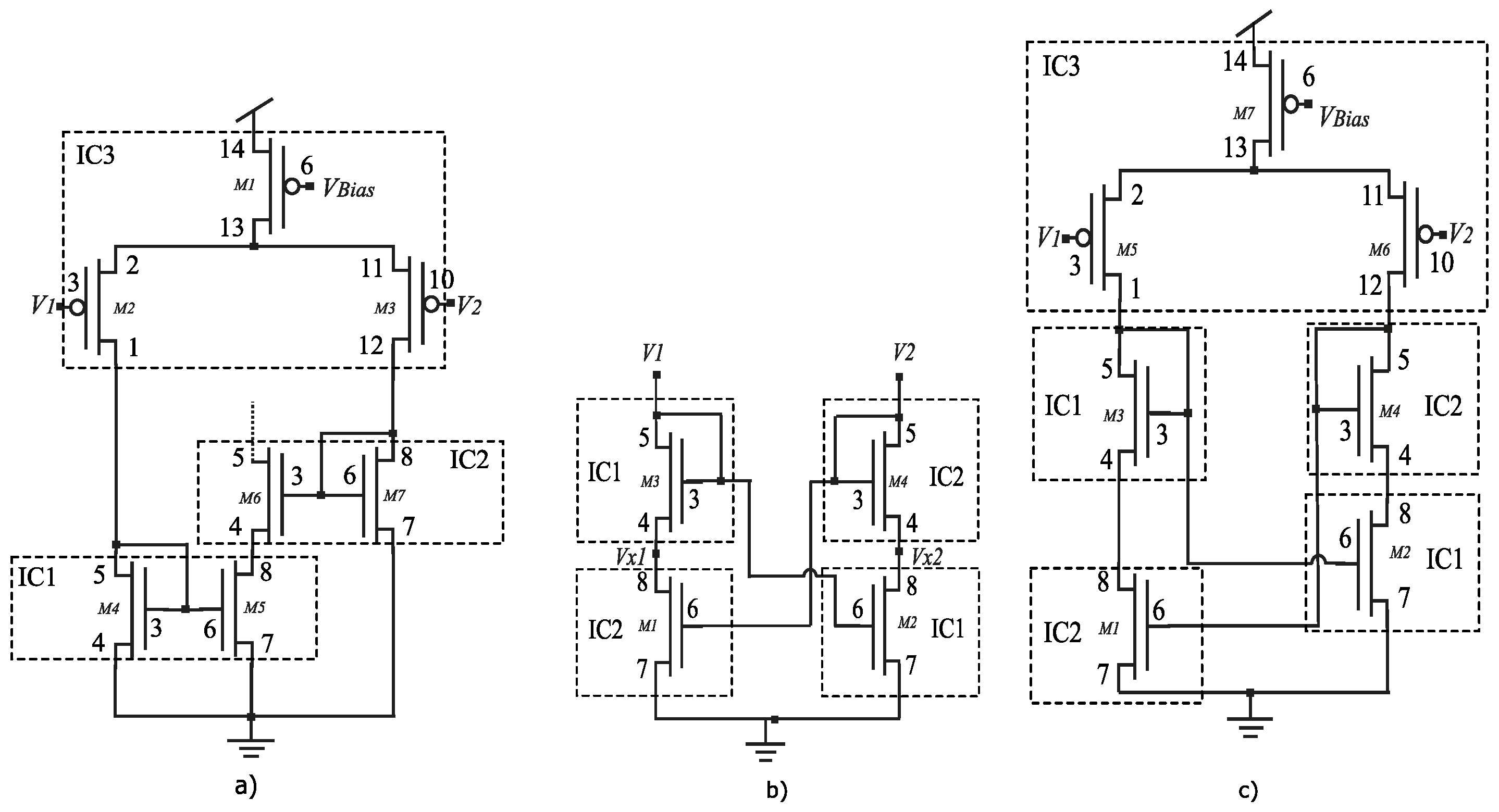
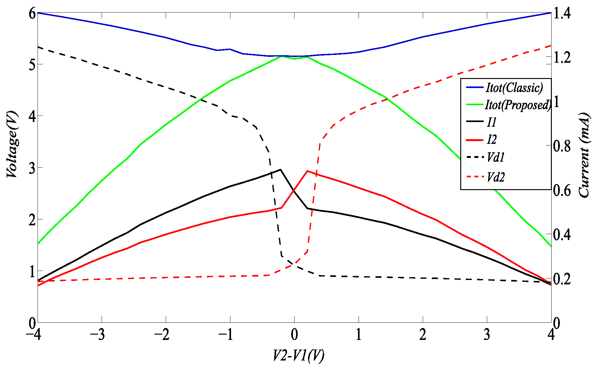
We could not measure the currents in each leg using the ASIC; therefore, all the circuits were implemented using the IC C D 4007 U B E from Texas Instruments. Using this IC did not allow for sizing the transistors for optimal design and the measurements only serve the purpose of proving the concept. To realize the different circuits, we had to use more than one chip. The circuit in Figure 1 was realized using two chips as shown in Figure 19b and tested by applying differential input voltages V 1 and V 2 in the range [ 2   V 6   V ] with input common-mode voltage at V i c m = 4 V. Measurement results for this circuit are shown in Figure 20. These measurement results provide the same wave forms obtained by the simulations in Figure 3, i.e., minimum currents I 1 , I 2 at the maximum distance between the two input signals ( V 1 = 2   V , V 2 = 6   V , and V 1 = 6   V , V 2 = 2 V) and a maximum correlation of I 1 and I 2 when V 1 = V 2 = 4 V.
Next, the measurement results for the circuit combining the correlator circuit and a different pair as shown in Figure 19a are shown in Figure 21. These measurement results also match the simulations shown in Figure 6. It is interesting to note that this behavior of currents in the two legs matches the one presented in Figure 7 for device widths equal to 1 μ m in the current mirror. The figure shows also the total power consumption of the classic bump circuit realized using the 3 ICs. We can see that the power consumption reduces by almost 72 percent compared to the classic bump when the difference between the input voltages is 4 V.

5. Double Charge Pump Interface with Bump Circuits

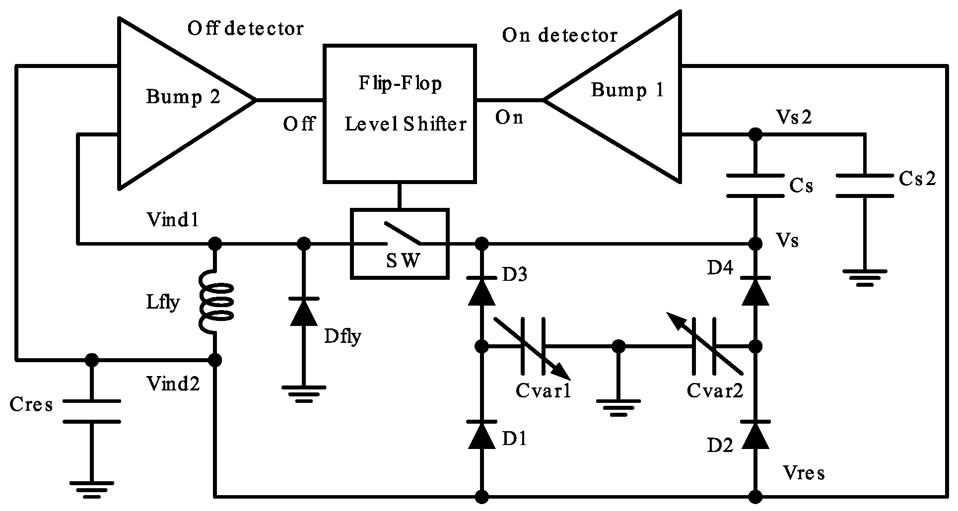
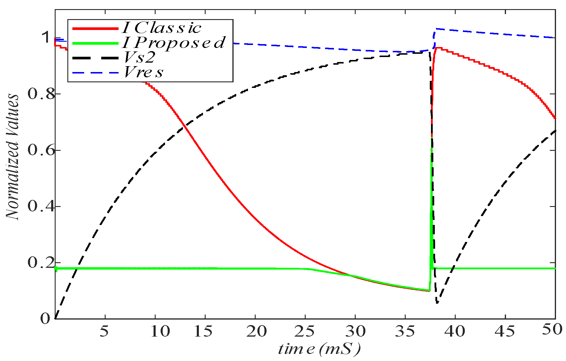
In the low power interface for a energy harvesting double charge pump proposed in Reference [9], the authors use two bump circuits for activating and deactivating the flyback switch, as shown in Figure 22. Capacitors Cvar 1 and Cvar 2 work deferentially and pump charges from the reservoir capacitance C r e s to the series connected capacitors C s and C s 2 . As the charges are being pumped, the voltage across C s and C s 2 increase. C s 2 is chosen much smaller than C s and when the voltage across C s 2 reaches the voltage at C r e s , the bump circuit 1 activates the flyback switch which transfers the charges to C r e s through the inductor L f l y . The voltage V S 2 is shown in Figure 23 as the dashed black curve and V r e s as the dashed blue curve. We compared the proposed bump circuit and classic one with each other for this application through simulation. The green and red solid curves are the current consumption of the proposed and classic bump circuits, respectively. The proposed bump circuit consumes almost 3.5 times less power consumption on average in this operation. After the switch goes on, the charges will flow from C s to C r e s . V S approaches the voltage across the C r e s , and the bump circuit 2 turns off the switch. This voltage change tends to be large and abrupt. This operation will take advantage of the variable power behavior of the proposed bump circuit. More detailed description of this charge pump is found in Reference [9].

6. Conclusions

In this paper, we presented a bump circuit, which finds the similarity between two voltages based on a novel voltage correlator. The proposed bump circuit offers the same properties of the classic bump circuit with the main difference that the current consumption approaches zero as the inputs become different. When the input voltages approach each other, currents flow increases, which also increases sensitivity. The simulations and measurements proved that the proposed bump circuit can use several orders of magnitude less power than classic bump circuit at maximum. Applications where similarity of two voltages is normally large, such as the low power interface for a charge pump presented, exploit the low power properties of the circuit at maximum. The proposed bump circuit was analyzed using simulation and measurements for proving the concept.

Author Contributions

M.A., L.M., and Y.B. contributed to problem formulation, conceptualization and choice of methods. M.A. performed all calculations, simulations, measurements and original draft preparation. L.M. performed the measurement of discrete components and contributed to the writing. M.A., L.M., and Y.B. contributed to interpretation of results, and to editing into the final manuscript. All authors have read and agreed to the published version of the manuscript.

Funding

This research received no external funding.

Conflicts of Interest

The authors declare no conflict of interest.

References

  1. Bubb, F.W. A Circuit for Generating Polynomials and Finding Their Zeros. Proc. IRE 1951, 39, 1556–1561. [Google Scholar] [CrossRef]
  2. Jung, W. Op Amp Applications Handbook; Newnes/Elsevier: Amsterdam, The Netherlands, 2005. [Google Scholar]
  3. Ragazzini, J.R.; Randall, R.H.; Russell, F.A. Analysis of Problems in Dynamics by Electronic Circuits. Proc. IRE 1947, 35, 444–452. [Google Scholar] [CrossRef]
  4. Popa, C. Low-power low-voltage CMOS analog signal processing circuits using a functional core. In Proceedings of the 2016 IEEE International Conference on Electronics, Circuits and Systems, Monte Carlo, Monaco, 11–14 December 2016. [Google Scholar]
  5. Bryant, M.D.; Yan, S.; Tsang, R.; Fernandez, B.; Kumar, K.K. A Mixed Signal (Analog-Digital) Integrator Design. IEEE Trans. Circuits Syst. I Regul. Pap. 2012, 59, 1409–1417. [Google Scholar] [CrossRef]
  6. Hiratkar, S.; Tijare, A.; Dakhole, P. VLSI design of analog multiplier in weak inversion region. In Proceedings of the 2016 International Conference on Communication and Signal Processing (ICCSP), Melmaruvathur, India, 6–8 April 2016. [Google Scholar]
  7. Liu, S.C. Analog VLSI: Circuits and Principles. In Bradford Book; MIT Press: Cambridge, MA, USA, 2002; Chapter 6; p. 168. [Google Scholar]
  8. Delbruck, T. Bump circuits for computing similarity and dissimilarity of analog voltages. In Proceedings of the International Joint Conference on Neural Networks, Seattle, WA, USA, 8–12 July 2019; pp. 475–479. [Google Scholar]
  9. Phan, T.N.; Azadmehr, M.; Le, C.P.; Halvorsen, E. Low power electronic interface for electrostatic energy harvesters. J. Phys. Conf. Ser. 2015, 660, 012087. [Google Scholar] [CrossRef]
  10. Theogarajan, L.; Akers, L.A. Novel circuits for neural information processing. J. Comput. Electr. Eng. 1999, 25, 409–420. [Google Scholar] [CrossRef]
  11. Azadmehr, M.; Abrahamsen, J.P.; Hafliger, P. A foveated AER imager chip. In Proceedings of the 2005 IEEE International Symposium on Circuits and Systems (ISCAS), Kobe, Japan, 23–26 May 2005. [Google Scholar]
  12. Lu, J.; Yang, T.; Jahan, M.S.; Holleman, J. Nano-power tunable bump circuit using wide-input-range pseudo-differential transconductor. Electron. Lett. 2014, 50, 921–923. [Google Scholar] [CrossRef] [Green Version]
  13. Peng, S.Y.; Minch, B.A.; Hasler, P. A programmable floating-gate bump circuit with variable width. IEEE Int. Symp. Circuits Syst. 2005, 5, 4341–4344. [Google Scholar]
  14. Bragg, J.A.; Brown, E.A.; Deweerth, S.P. A Tunable Voltage Correlator. Analog. Integr. Circuits Signal Process. 2004, 39, 89–94. [Google Scholar] [CrossRef]
  15. Lin, S.Y.; Huang, R.J.; Chiueh, T.D. A tunable Gaussian/square function computation circuit for analog neural networks. IEEE Trans. Circuits Syst. II Analog. Digit. Signal Process. 1998, 45, 441–446. [Google Scholar] [CrossRef]
  16. Minch, B.A. A simple variable-width CMOS bump circuit. In Proceedings of the 2016 IEEE International Symposium on Circuits and Systems (ISCAS), Montreal, QC, Canada, 22–25 May 2016; pp. 1354–1357. [Google Scholar]
  17. Azadmehr, M.; Marchetti, L.; Berg, Y. A low power analog voltage similarity circuit. In Proceedings of the 2017 IEEE International Symposium of Circuits and Systems (ISCAS), Baltimore, MD, USA, 28–31 May 2017. [Google Scholar]
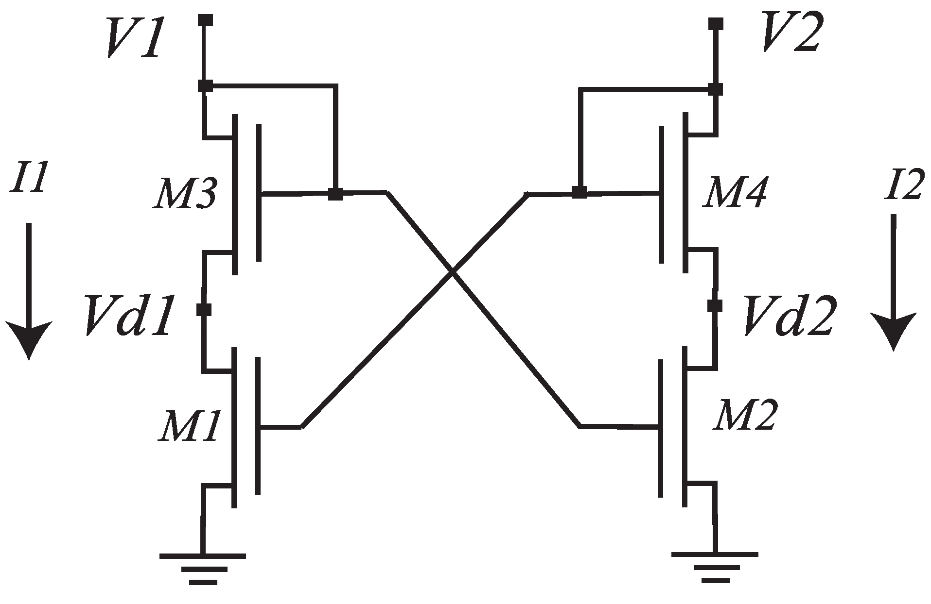
Figure 1. The proposed voltage correlator, where the currents I 1 and I 2 approach their maximum values when voltages V 1 and V 2 become equal.
Electronics 10 01141 g001
Figure 2. A simplified circuit when V 1 becomes larger than V 2 . In this case, M 4 is omitted as it is in deep triode ( V 1 > > V 2 ) , and the circuit behaves as a simple current mirror.
Electronics 10 01141 g002
Figure 3. Simulation of currents I 1 and I 2 when the widths of the transistors M 1 and M 2 are increased from 1 μ m to 10 μ m simultaneously with a common-mode voltage of V d d / 2 . The curves are normalized for the maximum value of the currents in the legs. The dashed curves are the sum of the normalized currents which has a bell shape.
Electronics 10 01141 g003
Figure 4. Simulation results of voltages V d 1 and V d 2 when the widths of the transistors M 1 and M 2 are increased from 1 μ m to 10 μ m simultaneously.
Electronics 10 01141 g004
Figure 5. (a) Stacking of a PMOS differential pair and the proposed correlator circuit. The behavior of currents I c 1 and I c 2 is a combination of the current behavior of the correlator and a differential pair. (b) Circuit model of the combined circuit when V2 increases and V1 decreases.
Electronics 10 01141 g005
Figure 6. Simulation of the currents Ic1 and Ic2 in the circuits shown in Figure 5 as black curves. The currents in the circuit in Figure 1 and a differential pair with resistive load are also presented for comparison. The dashed curves are the currents through the right leg of the circuit, and the solid curves are the currents in left leg. All the curves are normalized by their maximum value.
Electronics 10 01141 g006
Figure 7. Simulation result of the circuit shown in Figure 5a. The widths of transistors M 1 and M 2 are increased from 1 μ m to 10 μ m simultaneously as marked by the arrows and M 3 and M 4 have a constant width of 1 μ m. The total current Itot, which is the sum of the two currents is shown as dashed curves with a clear bell shape.
Electronics 10 01141 g007
Figure 8. Schematic of (a) the proposed bump circuit and (b) the classic bump circuit presented by Tobias Delbrück.
Electronics 10 01141 g008
Figure 9. Simulation result of voltages V A and V B in Figure 8a and Voltages V C and V D in Figure 8b.
Electronics 10 01141 g009
Figure 10. Comparison of the currents in the proposed bump circuit and the classic bump circuit. The black curves are the normalized currents in the classic bump circuit and the red curves the currents in the proposed circuit. The dashed curves are the output currents.
Electronics 10 01141 g010
Figure 11. Total static current consumption for all the input voltage combinations for the proposed bump circuit (a) and the classic bump circuit (b). The ratio between the total static power consumption of the classic and the proposed power bump circuit is shown in (c).
Electronics 10 01141 g011
Figure 12. The curves show the sensitivity of the proposed bump circuit when the two inputs have common-mode value increasing from 0 to V d d . The bias voltage is 2.6 V in this simulation.
Electronics 10 01141 g012
Figure 13. Simulation of total current for similarities between inputs at common-mode voltages 0 V, 0.5 V, 1 V, 1.5 V, 2 V, 2.5 V, and 3 V. The bias voltage is 2.6 V in this simulation. Arrows show the F W H M for each common-mode value.
Electronics 10 01141 g013
Figure 14. The power effectiveness and consumption is depending on the common-mode voltage of the input signals. The circuit is most effective regarding the power consumption when the common-mode is close to V d d = 3.2 V.
Electronics 10 01141 g014
Figure 15. (a) Micrograph of the chip produced using the 350 nm CMOS from AMS. Each node named in the picture is according the circuit shown in Figure 8a. Buffer1 is connected to VA and Buffer2 to Vout. (b) the measurement setup on PCB.
Electronics 10 01141 g015
Figure 16. Measurement results of VA and Vout at 10 kHz frequency. The dashed black curve is the simulation result with same parameters.
Electronics 10 01141 g016
Figure 17. Measurement and simulation results of total power consumption when V 2 is 0 V and V 1 increases from G n d to V d d .
Electronics 10 01141 g017
Figure 18. Measurement result of the total power consumption when V 1 decreases from V d d / 2 to zero and V 2 increases from V d d / 2 to V d d simultaneously.
Electronics 10 01141 g018
Figure 19. Pin numbers and connections diagram for the IC C D 4007 U B E to realize (a) the classic bump using 2 ICs (b) voltage correlator using 3 ICs and (c) the proposed bump connection using 3 ICs. Bulks of NMOS are connected to G N D and PMOS to V D D .
Electronics 10 01141 g019
Figure 20. Measurement results for the circuit in Figure 1. The differential input signals V 1 and V 2 are varied in a range [2 V–6 V] with a step of |0.1 V| and characterized by an input common-mode of 4 V.
Electronics 10 01141 g020
Figure 21. Measurement results for the proposed bump circuit with input differential pair. The differential input signals V 1 and V 2 are varied in a range [4 V–8 V] with a step of |0.1 V| and characterized by an input common-mode of 6 V. V B i a s = 7 V.
Electronics 10 01141 g021
Figure 22. Simplified schematic of a double charge pump that uses two bump circuits to control the switch in the flyback.
Electronics 10 01141 g022
Figure 23. Comparison of the total currents absorbed by the classic bump circuit (red curve) with a average of 8.44 μ A and the proposed bump circuit (green curve) 2.33 μ A used in a double charge pump shown in Figure 22 as on detector. The black dashed line is the voltage V r e s , and the blue dashed curves is the voltages V s 2 .
Electronics 10 01141 g023
Table 1. Comparison of bump circuits. <Nr of devices> in the table is the minimum number of devices needed to realize the circuit. Results from “[8]” in the figure below are from the presented work.
Ref.This Work[8][12][13][14][15][16]
Vdd (V)3.23.2325 ± 2.5 5
Power (W)256 n256 n18.9 nnananana
Technology350 nm 350 nm 500 nm 1.2 μ m500 nm 3 μ mALD1106/7
Nr of devices1081815111411
Publisher’s Note: MDPI stays neutral with regard to jurisdictional claims in published maps and institutional affiliations.