
Linear Active Disturbance Rejection Control Strategy with Known Disturbance Compensation for Voltage-Controlled Inverter


Abstract
1. Introduction
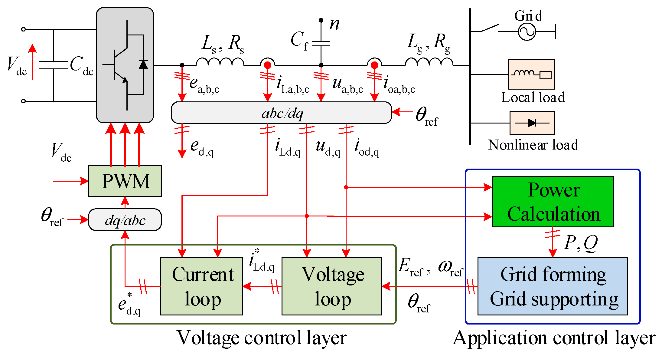
2. Modeling and Control of Inverters
2.1. Inverter Modelling in SRF
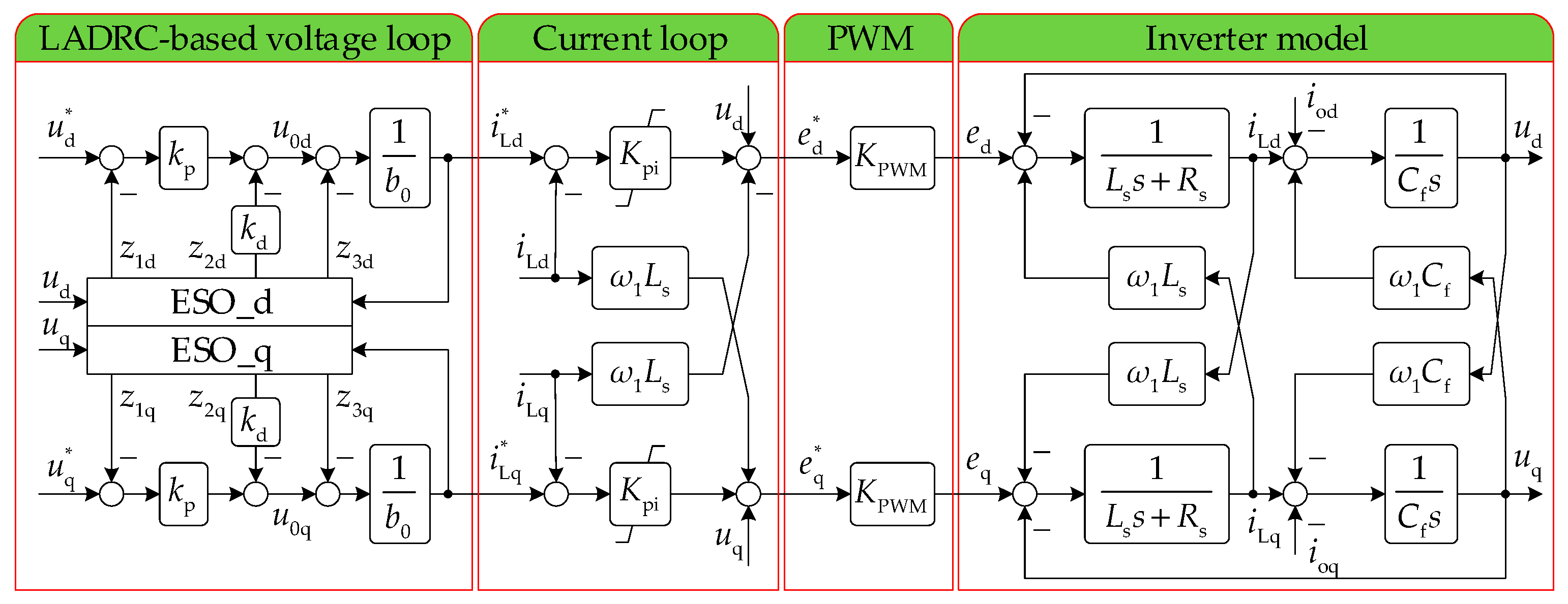
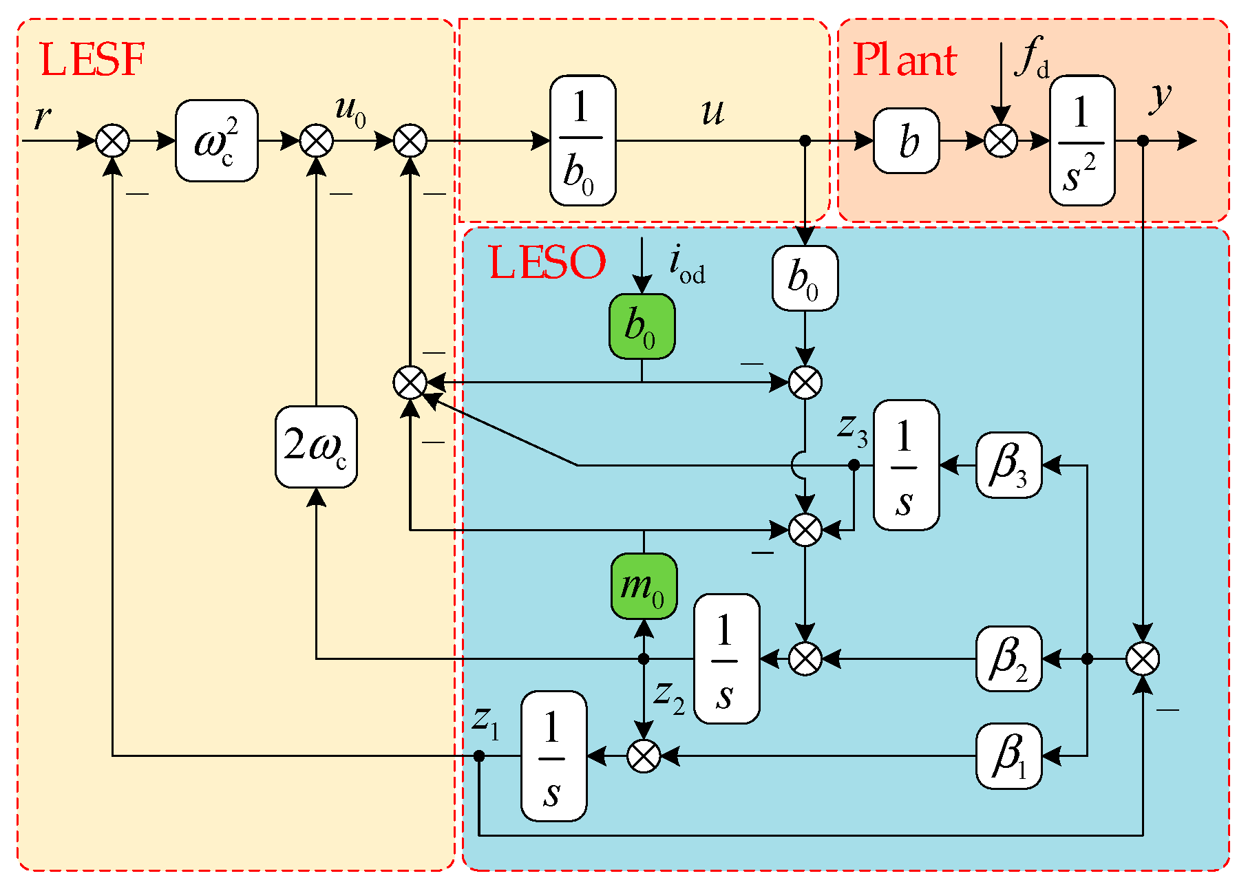
2.2. Structure of LADRC-Based Voltage Loop
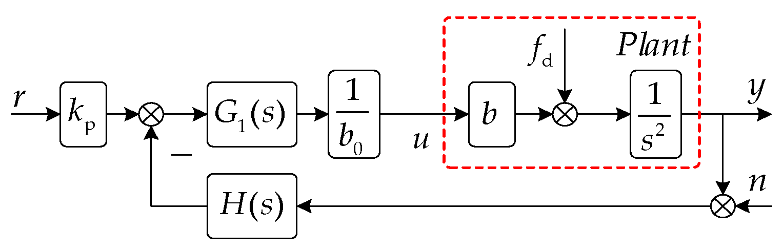
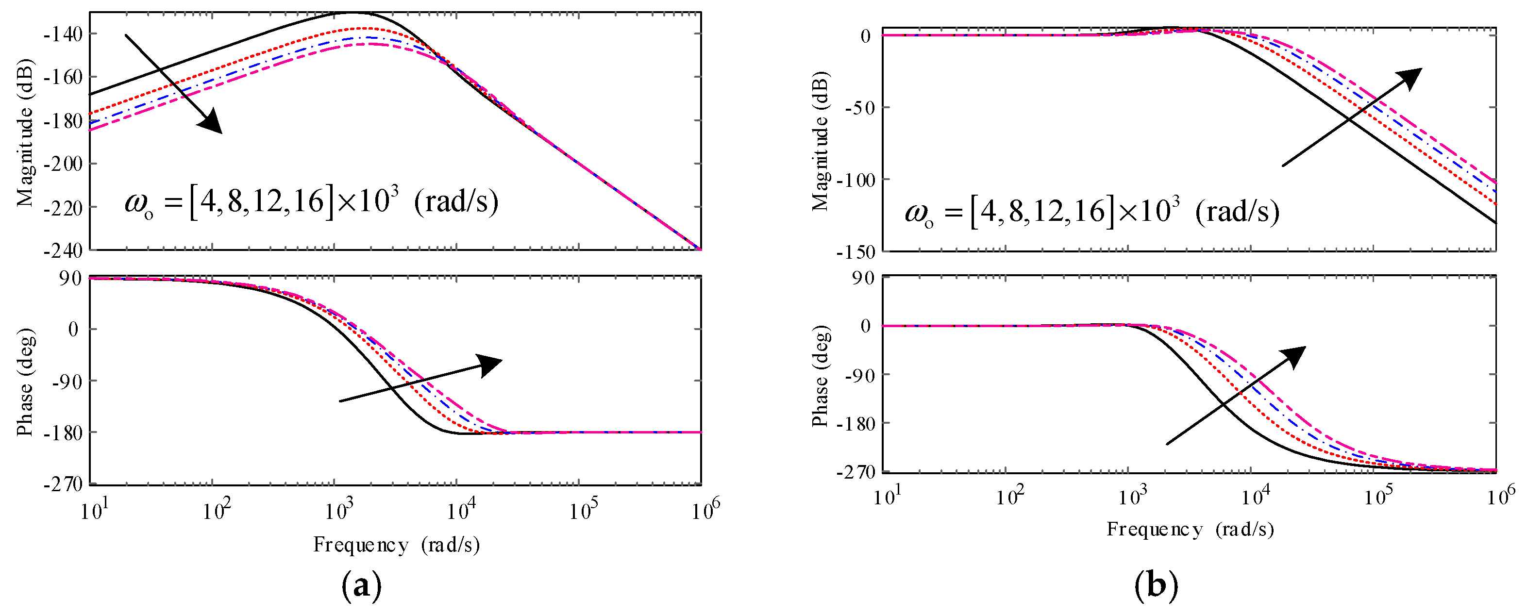
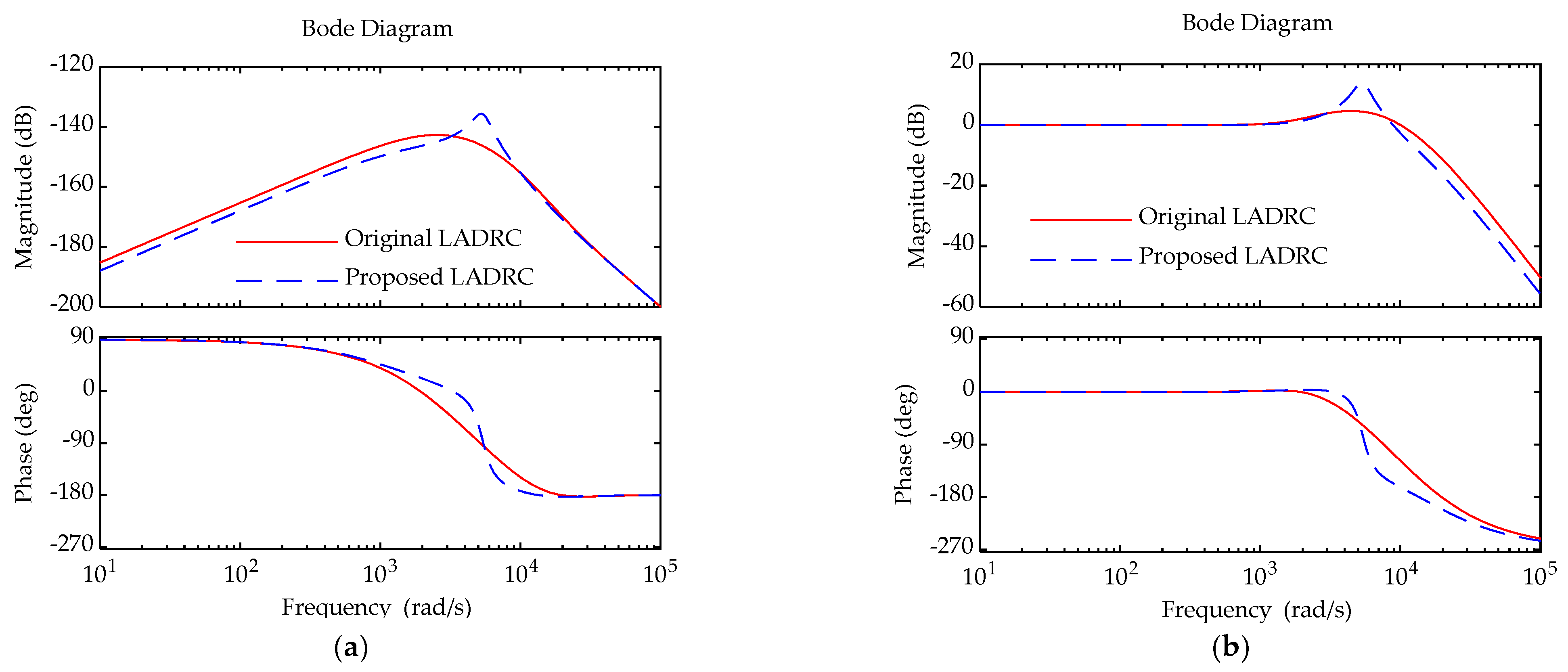
2.3. Influence of Observer Bandwidth and Compensation Factor
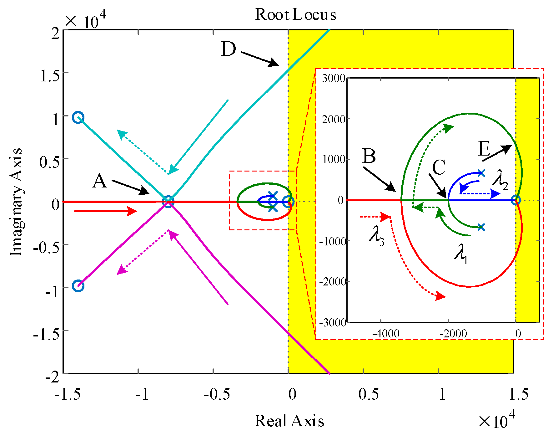
- When , the poles are located at points A and C on the real axis, corresponding to and , and the system has no overshoot and a short settling time;
- When changes from 0 to infinite, if is smaller than 1.02 (point D), or greater than 5.24 (point E), the system will be unstable. The range of that makes the system stable is listed in Table 1. As increases, the stable range of is expanded.
- When increases from 0 to 1, poles enter the stable regions and approach point A and C. Poles , , and are closer to the imaginary axis, so are marked as dominant poles. With increasing, and gradually move away from the imaginary axis and approach the real axis, so the response time and overshoot decreases and the damping increases.
- When increases from 1 to 1.02 (point B), , , and are on the real axis and there is no overshoot in response. When they continue to increase, poles approach the imaginary axis, and the damping becomes smaller. This shows that the response becomes slower, and there is both overshoot and damped oscillation, then poles cross the negative half axis, and the system becomes unstable.
3. Known Disturbance Compensation Scheme
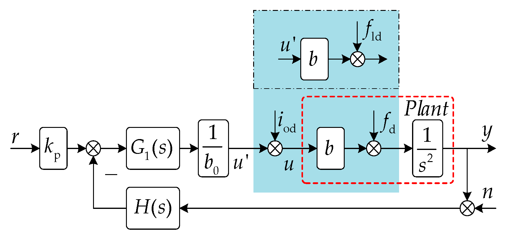
3.1. Design of Proposed Scheme
3.2. Analysis of the Proposed Scheme
3.3. Stability Analysis
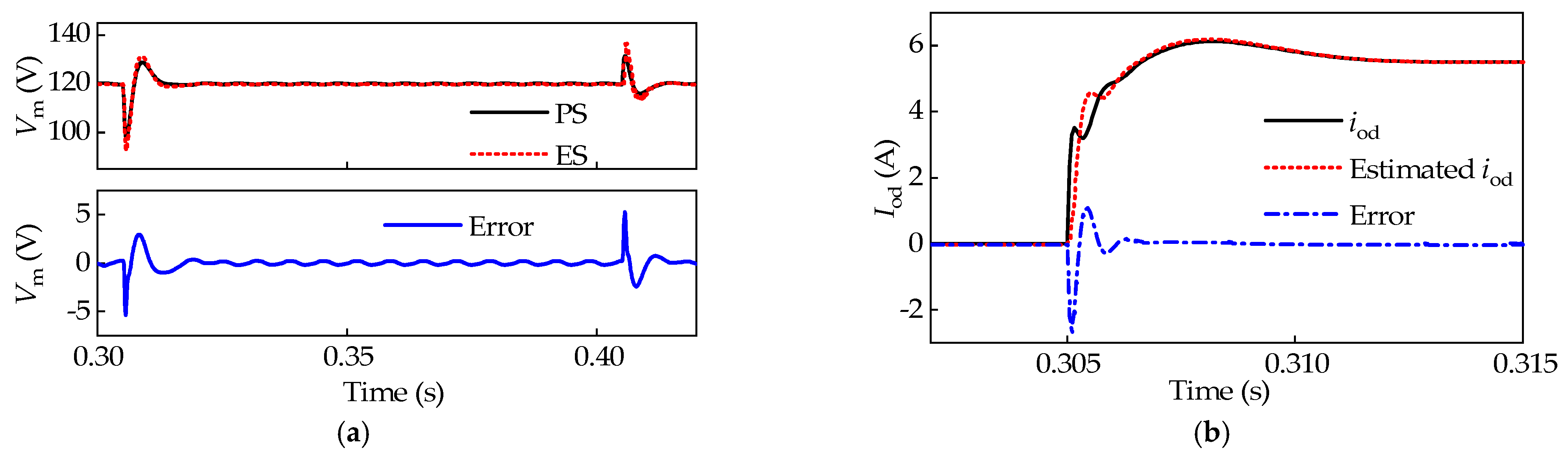
3.4. Load Current Estimator
4. Simulation and Experimental Verification
4.1. Discretization of LESO
4.2. Simulation Results
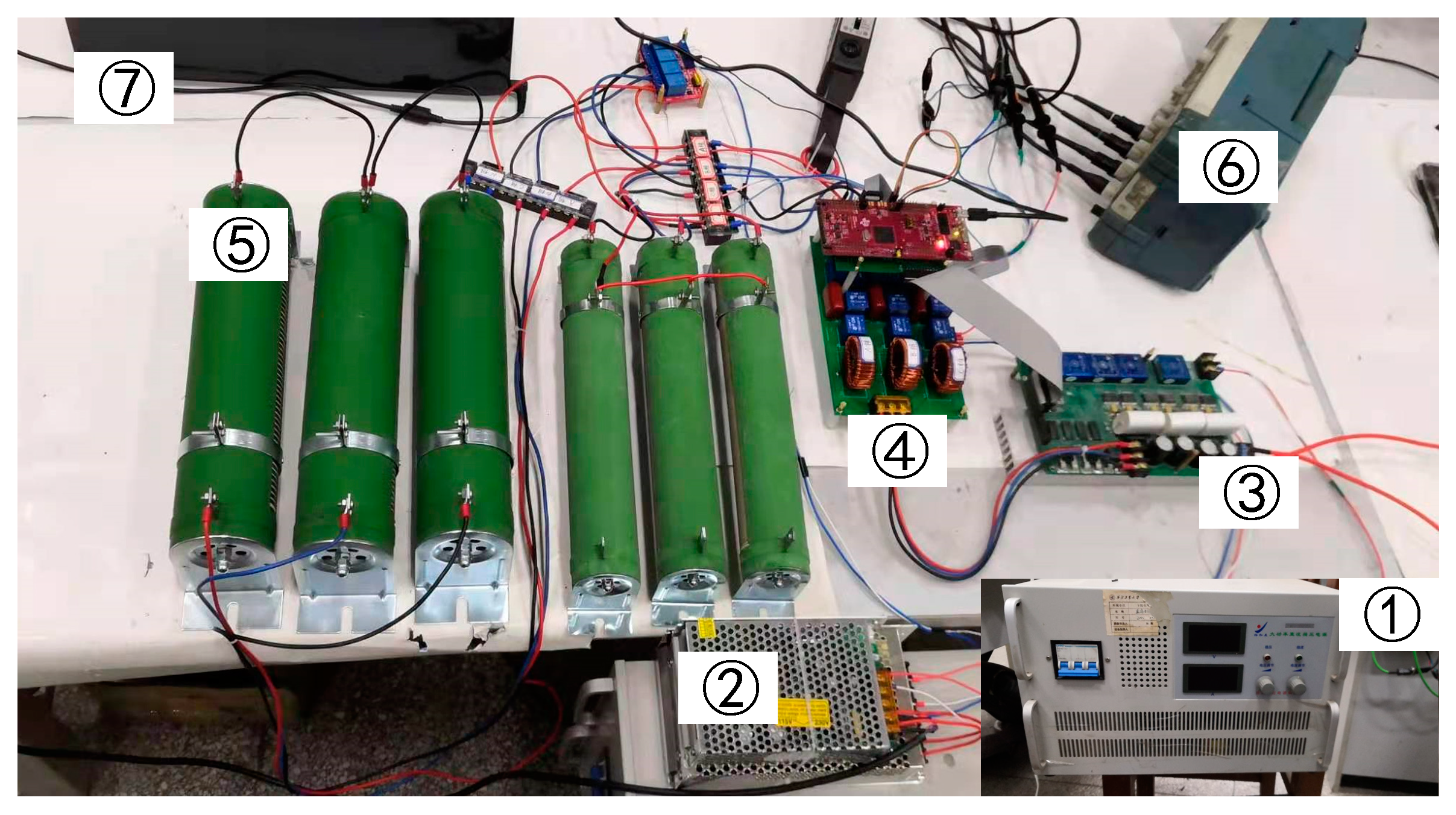
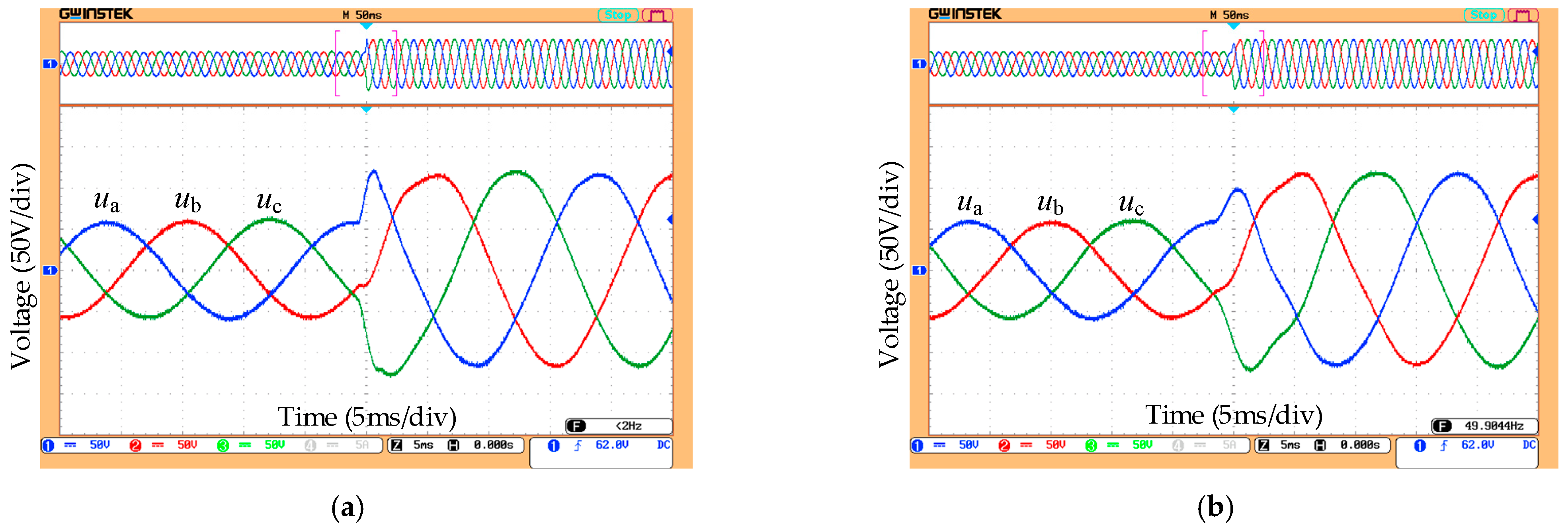
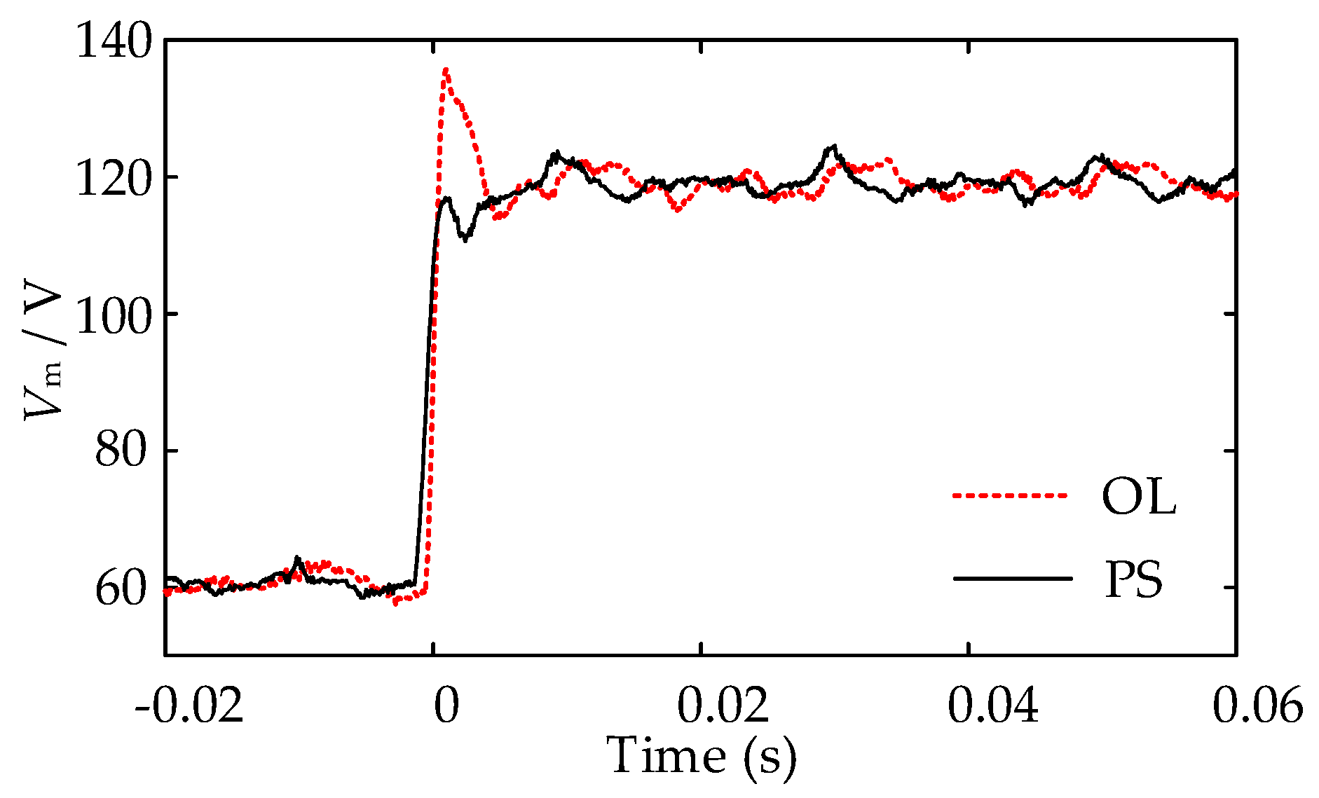
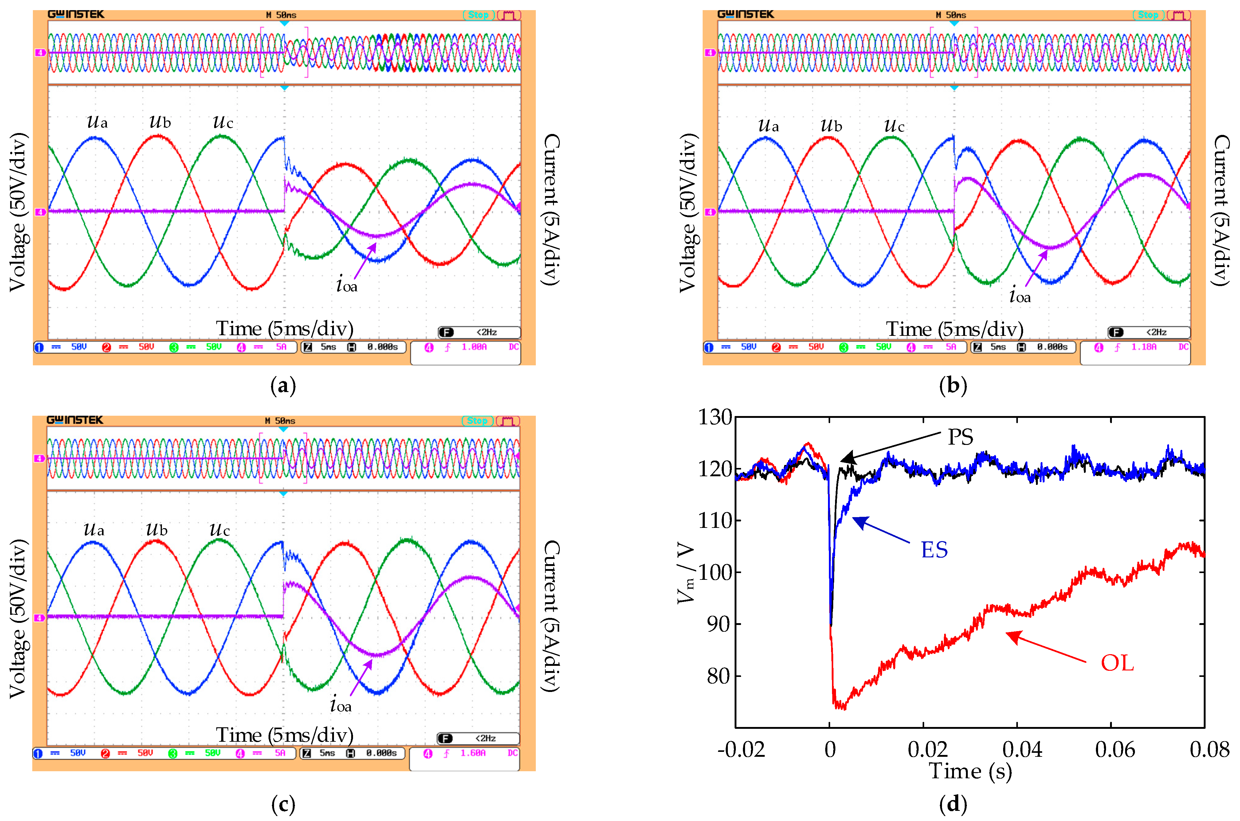
4.3. Experiment Results
5. Conclusions
Author Contributions
Funding
Conflicts of Interest
Abbreviations
| Acronym | Definition |
| LADRC | Linear active disturbance rejection control |
| VCI | Voltage-controlled inverter |
| LESO | Linear extended state observer |
| DERs | Distributed energy resources |
| RES | Renewable energy sources |
| MG | Microgrid |
| PI | Proportional-integral |
| PWM | Pulse width modulation |
| THD | Total harmonic distortion |
| RC | Repetitive control |
| LSEF | Linear state error feedback |
| SRF | Synchronous reference frame |
| PCC | Point of common coupling |
| CG | Control gain |
| CF | Compensation factor |
| LPF | Low-pass filter |
| BTM | Bilinear transformation method |
References
- Hosseinzadeh, N.; Aziz, A.; Mahmud, A.; Gargoom, A.; Rabbani, M. Voltage Stability of Power Systems with Renewable-Energy Inverter-Based Generators: A Review. Electronics 2021, 10, 115. [Google Scholar] [CrossRef]
- Arbab-Zavar, B.; Palacios-Garcia, E.; Vasquez, J.; Guerrero, J. Smart Inverters for Microgrid Applications: A Review. Energies 2019, 12, 840. [Google Scholar] [CrossRef]
- Hossain, M.A.; Pota, H.R.; Issa, W.; Hossain, M.J. Overview of AC microgrid controls with inverter-interfaced generations. Energies 2017, 10, 1300. [Google Scholar] [CrossRef]
- Rocabert, J.; Luna, A.; Blaabjerg, F.; Rodríguez, P. Control of Power Converters in AC Microgrids. IEEE Trans. Power Electron. 2012, 27, 4734–4749. [Google Scholar] [CrossRef]
- Bouzid, A.M.; Guerrero, J.M.; Cheriti, A.; Bouhamida, M.; Sicard, P.; Benghanem, M. A survey on control of electric power distributed generation systems for microgrid applications. Renew. Sustain. Energy Rev. 2015, 44, 751–766. [Google Scholar] [CrossRef]
- Quan, X.; Dou, X.; Wu, Z.; Hu, M.; Song, H.; Huang, A.Q. A Novel Dominant Dynamic Elimination Control for Voltage-Controlled Inverter. IEEE Trans. Ind. Electron. 2018, 65, 6800–6812. [Google Scholar] [CrossRef]
- Dou, C.; Zhang, Z.; Yue, D.; Song, M. Improved droop control based on virtual impedance and virtual power source in low-voltage microgrid. IET Gener. Transm. Distrib. 2017, 11, 1046–1054. [Google Scholar] [CrossRef]
- Buso, S.; Caldognetto, T.; Brandao, D.I. Dead-beat current controller for voltage source converters with improved large-signal response. IEEE Trans. Ind. Appl. 2015, 52, 1588–1596. [Google Scholar] [CrossRef]
- Lim, K.; Choi, J. Seamless Grid Synchronization of a Proportional+Resonant Control-Based Voltage Controller Considering Non-Linear Loads under Islanded Mode. Energies 2017, 10, 1514. [Google Scholar] [CrossRef]
- Komurcugil, H.; Altin, N.; Ozdemir, S.; Sefa, I. Lyapunov-Function and Proportional-Resonant-Based Control Strategy for Single-Phase Grid-Connected VSI with LCL Filter. IEEE Trans. Ind. Electron. 2016, 63, 2838–2849. [Google Scholar] [CrossRef]
- Zhang, M.; Huang, L.; Yao, W.; Lu, Z. Circulating Harmonic Current Elimination of a CPS-PWM-Based Modular Multilevel Converter With a Plug-In Repetitive Controller. IEEE Trans. Power Electron. 2014, 29, 2083–2097. [Google Scholar] [CrossRef]
- Marati, N.; Prasad, D. A Modified Feedback Scheme Suitable for Repetitive Control of Inverter With Nonlinear Load. IEEE Trans. Power Electron. 2018, 33, 2588–2600. [Google Scholar] [CrossRef]
- Yaramasu, V.; Rivera, M.; Narimani, M.; Wu, B.; Rodriguez, J. Model Predictive Approach for a Simple and Effective Load Voltage Control of Four-Leg Inverter With an Output LC Filter. IEEE Trans. Ind. Electron. 2014, 61, 5259–5270. [Google Scholar] [CrossRef]
- Mahdian Dehkordi, N.; Sadati, N.; Hamzeh, M. A backstepping high-order sliding mode voltage control strategy for an islanded microgrid with harmonic/interharmonic loads. Control Eng. Pract. 2017, 58, 150–160. [Google Scholar] [CrossRef]
- Komurcugil, H. Improved passivity-based control method and its robustness analysis for single-phase uninterruptible power supply inverters. IET Power Electron. 2015, 8, 1558–1570. [Google Scholar] [CrossRef]
- Rymarski, Z.; Bernacki, K.; Dyga, Ł.; Davari, P. Davari Passivity-Based Control Design Methodology for UPS Systems. Energies 2019, 12, 4301. [Google Scholar] [CrossRef]
- Han, J. From PID to Active Disturbance Rejection Control. IEEE Trans. Ind. Electron. 2009, 56, 900–906. [Google Scholar] [CrossRef]
- Gao, Z. Active disturbance rejection control: A paradigm shift in feedback control system design. In Proceedings of the 2006 American Control Conference, Minneapolis, MN, USA, 14–16 June 2006; p. 7. [Google Scholar] [CrossRef]
- Benrabah, A.; Xu, D.; Gao, Z. Active Disturbance Rejection Control of LCL-Filtered Grid-Connected Inverter Using Padé Approximation. IEEE Trans. Ind. Appl. 2018, 54, 6179–6189. [Google Scholar] [CrossRef]
- Zhang, H.; Xian, J.; Shi, J.; Wu, S.; Ma, Z. High Performance Decoupling Current Control by Linear Extended State Observer for Three-Phase Grid-Connected Inverter With an LCL Filter. IEEE Access 2020, 8, 13119–13127. [Google Scholar] [CrossRef]
- Cao, Y.; Zhao, Q.; Ye, Y.; Xiong, Y. ADRC-Based Current Control for Grid-Tied Inverters: Design, Analysis, and Verification. IEEE Trans. Ind. Electron. 2020, 67, 8428–8437. [Google Scholar] [CrossRef]
- Zhang, Y.; Zhu, J.; Dong, X.; Zhao, P.; Ge, P.; Zhang, X. A Control Strategy for Smooth Power Tracking of a Grid-Connected Virtual Synchronous Generator Based on Linear Active Disturbance Rejection Control. Energies 2019, 12, 3024. [Google Scholar] [CrossRef]
- Yu, Y.; Hu, X. Active Disturbance Rejection Control Strategy for Grid-Connected Photovoltaic Inverter Based on Virtual Synchronous Generator. IEEE Access 2019, 7, 17328–17336. [Google Scholar] [CrossRef]
- Li, S.; Li, Y.; Chen, X.; Jiang, W.; Li, X.; Li, T. Control strategies of grid-connection and operation based on active disturbance rejection control for virtual synchronous generator. Int. J. Electr. Power Energy Syst. 2020, 123, 106144. [Google Scholar] [CrossRef]
- Ma, W.; Guan, Y.; Zhang, B. Active Disturbance Rejection Control Based Control Strategy for Virtual Synchronous Generators. IEEE Trans. Energy Convers. 2020, 35, 1747–1761. [Google Scholar] [CrossRef]
- Zeng, J.; Huang, Z.; Huang, Y.; Qiu, G.; Li, Z.; Yang, L.; Yu, T.; Yang, B. Modified linear active disturbance rejection control for microgrid inverters: Design, analysis, and hardware implementation. Int. Trans. Electr. Energy Syst. 2019, 29. [Google Scholar] [CrossRef]
- Li, H.; Li, S.; Lu, J.; Qu, Y.; Guo, C. A Novel Strategy Based on Linear Active Disturbance Rejection Control for Harmonic Detection and Compensation in Low Voltage AC Microgrid. Energies 2019, 12, 3982. [Google Scholar] [CrossRef]
- Wu, G.; Sun, L.; Lee, K.Y. Disturbance rejection control of a fuel cell power plant in a grid-connected system. Control Eng. Pract. 2017, 60, 183–192. [Google Scholar] [CrossRef]
- Zhou, R.; Tan, W. A generalized active disturbance rejection control approach for linear systems. In Proceedings of the IEEE 10th Conference on Industrial Electronics and Applications (ICIEA), Auckland, New Zealand, 15–17 June 2015; pp. 248–255. [Google Scholar] [CrossRef]
- Fu, C.; Tan, W. Tuning of linear ADRC with known plant information. ISA Trans. 2016, 65, 384–393. [Google Scholar] [CrossRef] [PubMed]
- Wu, Y.; Ye, Y. Internal Model-Based Disturbance Observer With Application to CVCF PWM Inverter. IEEE Trans. Ind. Electron. 2018, 65, 5743–5753. [Google Scholar] [CrossRef]
- Guo, L.; Li, Y.; Jin, N.; Dou, Z.; Wu, J. Sliding mode observer-based AC voltage sensorless model predictive control for grid-connected inverters. IET Power Electron. 2020, 13, 2077–2085. [Google Scholar] [CrossRef]
- Zheng, Q.; Dong, L.; Lee, D.H.; Gao, Z. Active Disturbance Rejection Control for MEMS Gyroscopes. IEEE Trans. Control Syst. Technol. 2009, 17, 1432–1438. [Google Scholar] [CrossRef]


| 2000 | 4000 | 2 | 0.247~4.11 |
| 2000 | 8000 | 4 | 0.208~5.24 |
| 2000 | 12,000 | 6 | 0.185~6.51 |
| Symbol | Quantity | Value |
|---|---|---|
| DC bus voltage | 300 V | |
| Filter inductor | 3.0 mH | |
| Inductor resistor | 0.16 Ω | |
| Filter capacitor | 14 μF | |
| Switching frequency | 10 kHz | |
| Sampling period | 100 μs | |
| Voltage amplitude/frequency | 120 V/50 Hz | |
| The gain in the current loop | 18.8 | |
| Controller bandwidth in LADRC | 3142 rad/s | |
| Observer bandwidth in LADRC | 10,472 rad/s |
| Schemes | Voltage Drop (V) | Voltage Maximum (V) | Settling Time (ms) |
|---|---|---|---|
| OL | 48.47 | 19 | |
| MC | 51.51 | 21 | |
| LC | 99.62 | 130.62 | 8 |
| PS | 97.86 | 128.79 | 7 |
| Schemes | No Load (60 V) | No Load (120 V) | Full Load (120 V) |
|---|---|---|---|
| OL | 0.26 | 0.39 | 0.21 |
| MC | 0.23 | 0.34 | 0.18 |
| LC | 0.26 | 0.39 | 0.42 |
| PS | 0.23 | 0.35 | 0.34 |
| ES | 0.24 | 0.35 | 0.36 |
| Schemes | No Load (60 V) | No Load (120 V) | Full Load (120 V) |
|---|---|---|---|
| OL | 1.25 | 1.38 | 1.67 |
| PS | 0.85 | 0.89 | 1.86 |
| ES | 0.88 | 0.94 | 1.96 |
Publisher’s Note: MDPI stays neutral with regard to jurisdictional claims in published maps and institutional affiliations. |
© 2021 by the authors. Licensee MDPI, Basel, Switzerland. This article is an open access article distributed under the terms and conditions of the Creative Commons Attribution (CC BY) license (https://creativecommons.org/licenses/by/4.0/).
Share and Cite
Li, Y.; Qi, R.; Dai, M.; Zhang, X.; Zhao, Y. Linear Active Disturbance Rejection Control Strategy with Known Disturbance Compensation for Voltage-Controlled Inverter. Electronics 2021, 10, 1137. https://doi.org/10.3390/electronics10101137
Li Y, Qi R, Dai M, Zhang X, Zhao Y. Linear Active Disturbance Rejection Control Strategy with Known Disturbance Compensation for Voltage-Controlled Inverter. Electronics. 2021; 10(10):1137. https://doi.org/10.3390/electronics10101137
Chicago/Turabian StyleLi, Yang, Rong Qi, Mingguang Dai, Xi Zhang, and Yiyun Zhao. 2021. "Linear Active Disturbance Rejection Control Strategy with Known Disturbance Compensation for Voltage-Controlled Inverter" Electronics 10, no. 10: 1137. https://doi.org/10.3390/electronics10101137
APA StyleLi, Y., Qi, R., Dai, M., Zhang, X., & Zhao, Y. (2021). Linear Active Disturbance Rejection Control Strategy with Known Disturbance Compensation for Voltage-Controlled Inverter. Electronics, 10(10), 1137. https://doi.org/10.3390/electronics10101137