Article

Low-Cost Low-Power Acceleration of a Microwave Imaging Algorithm for Brain Stroke Monitoring

1
Department of Electronics and Telecommunications, Politecnico di Torino, Corso Duca degli Abruzzi 24, I-10129 Torino, Italy
2
Consiglio Nazionale delle Ricerche-Istituto per il Rilevamento Elettromagnetico dell’Ambiente (CNR-IREA), 80124 Napoli, Italy
*
Author to whom correspondence should be addressed.
J. Low Power Electron. Appl. 2018, 8(4), 43; https://doi.org/10.3390/jlpea8040043
Submission received: 26 September 2018 / Revised: 27 October 2018 / Accepted: 31 October 2018 / Published: 1 November 2018

Abstract

:
Microwave imaging can effectively image the evolution of a hemorrhagic stroke thanks to the dielectric contrast between the blood and the surrounding brain tissues. To keep low both the form factor and the power consumption in a bedside device, we propose implementing a microwave imaging algorithm for stroke monitoring in a programmable system-on-chip, in which a simple ARM-based CPU offloads to an FPGA the heavy part of the computation. Compared to a full-software implementation in the ARM CPU, we obtain a 5× speed increase with hardware acceleration without loss in accuracy and precision.

1. Introduction

Brain strokes, of either the hemorrhagic or the ischemic type, are among the most common causes of death or permanent disability, with more than 15 million newly affected people worldwide every year [1]. It is well known that rapidity of intervention and treatment are crucial for the effectiveness of the therapy. Monitoring the effect of the treatment in the post-acute stage is also very important. Monitoring is currently done with diagnostic techniques such as Magnetic Resonance Imaging (MRI) and Computerized Tomography (CT). These imaging techniques are not appropriate for frequent monitoring at the patient bedside. An appropriate monitoring device for the stroke follow-up would be characterized by small form factor, low power consumption, and cost effectiveness. MRI and CT do not possess these characteristics. In addition, frequently repeated exposure to ionizing radiations in CT can be harmful for the patient. Therefore, there is a need for new imaging methods and tools.
Microwave Imaging (MI) is a biomedical imaging technique that senses local variations of dielectric properties of tissues [2]. When tissues are hit by low-power electromagnetic microwaves emitted by a set of antennas, the scattered electromagnetic field is first acquired by the same antennas and then processed by algorithms that produce an image that highlight spatial changes in dielectric properties. In the case of brain strokes, what can be imaged are the local dielectric changes caused by the blood supply anomaly [3].
MI is safe as it uses low-power, non-ionizing microwaves. For this reason, MI has been proposed as a complementary technique for frequent screening of breast cancer [4]. Previous work in this field has shown that it is possible to leverage existing technology and commercial off-the-shelf components to build low-cost MI systems for breast cancer detection with small form factor and low power consumption [5,6,7].
These previous results on MI for breast cancer and the recent work on the effectiveness of MI for stroke monitoring (e.g., [8]) encouraged us to undertake the research endeavor that we report in this paper. Here, we focus on one specific aspect of an MI system for stroke monitoring: how to design the processing subsystem that elaborates the signals received from the antennas and generates the medical images in such a way to keep low the power consumption, the form factor, and the cost while guaranteeing a sufficiently fast response.
We found that a low-cost, low-power Programmable System-on-Chip (PSoC) in which the processor offloads the heavy part of the computation to a hardware accelerator implemented in a Field-Programmable Gate Array (FPGA) can perform the elaboration task at a speed 5× greater than what the processor achieves without hardware acceleration. This is obtained without changes in precision or accuracy. The coexistence of the processor and the accelerator in the same Xilinx Zynq chip with shared memory and the use of Linux OS facilitate the programming tasks and the reuse of code and software mathematical libraries. Compared to on a high-end Xeon Intel CPU, we obtain a significant increase of the performance-per-watt figure of merit, about 3.7× better.
The paper is organized as follows. In Section 2, we present the MI system, the MI algorithm and its software implementation. In Section 3, we present the design of the hardware accelerator. In Section 4, we compare the results obtained in the software implementation with those obtained in the hardware accelerated one. We review the related work in Section 5. Finally, Section 6 concludes the paper.

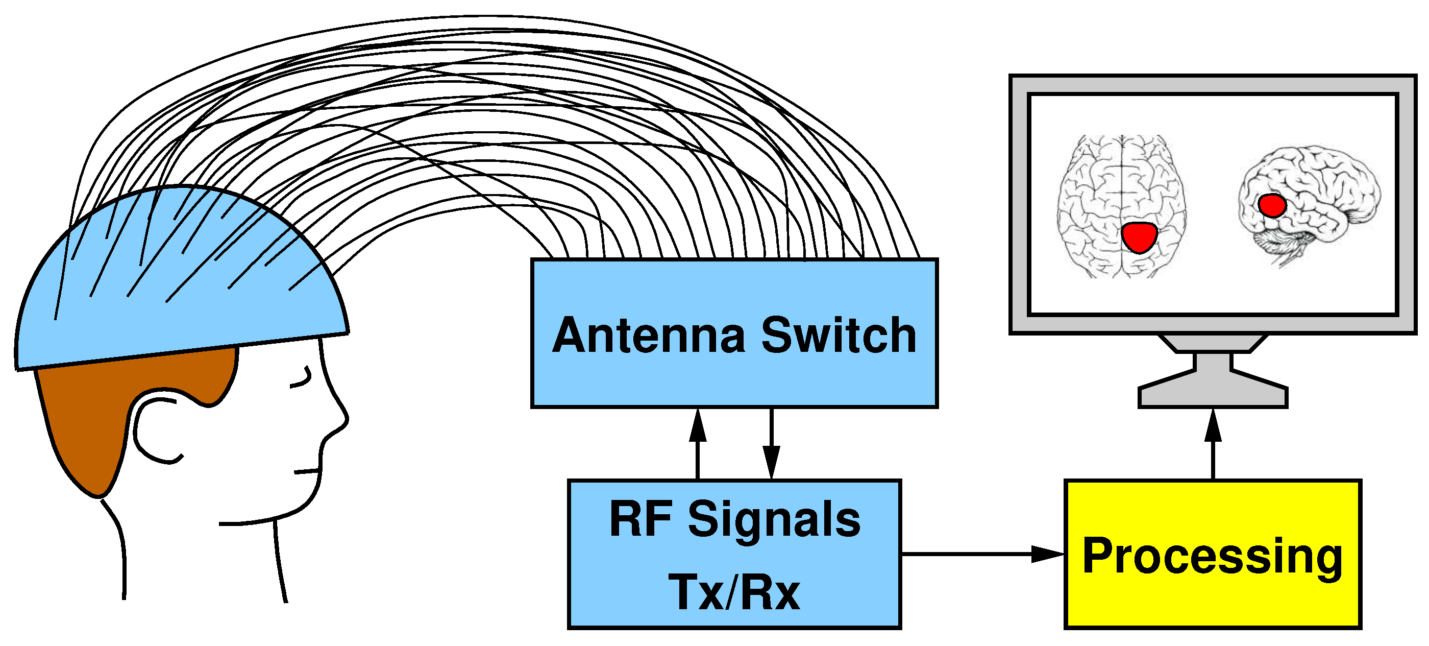
2. Stroke Monitoring Microwave Imaging System for Stroke Follow-Up Monitoring

The block scheme in Figure 1 shows the five main parts that compose our MI system for brain stroke monitoring: (I) a helmet containing the antennas; (II) a switch matrix in charge of routing the transmitted and received RF signals; (III) a Vector Network Analyzer (VNA) for transmitting and receiving signals; (IV) a dedicated hardware enabling the processing of the acquired data; and (V) a display showing the reconstructed image.
The helmet is made of plastic material and has many holes all around its surface, into which 24  antennas are wedged. The antennas are distributed all over the helmet surface to provide an uniform irradiation to the patient’s head. The antennas can operate both as transmitters and receivers. Indeed, the switching matrix has been designed to route the signal generated by the VNA to one single antenna keeping all the others as receivers. Since the VNA has two ports (one transmitting and one receiving), a controller configures the switch matrix in such a way that only one transmitter and one receiver can be simultaneously active and connected to the VNA. From the ratio between received and transmitted signals, the VNA derives the scattering parameters in terms of magnitude (i.e., attenuation) and phase shift, which are ultimately converted into complex numbers with a real part and an imaginary part.
A complete scan requires iterating until all 24 antennas are configured as transmitters and, for  each of these iterations, 24 different received signals are recorded (including the reflection captured by the same transmitting antenna). The scattering parameters obtained from a complete scan are stored by the VNA as a 24 × 24 matrix in a textual format. This file represents the input of the next stage: the image reconstruction algorithm, which is executed by the yellow processing block in Figure 1.

2.1. MI Algorithm

When monitoring the evolution of the stroke, scattering data are acquired periodically. The image reconstruction algorithm aims at detecting variations of the blood mass across two successive data acquisitions. The algorithm casts these variations as dielectric contrast changes Δ χ , which in turn determine variations Δ E S of the scattering matrices collected at two different time instants. Since such variations are small with respect to the size of the investigated region, which is supposed not to change, the imaging problem can be reliably linearized, by adopting the distorted Born approximation [9]:
Δ E S r p , r q = L Δ χ .
In Equation (1), L is a linear and compact integral operator relating the differential data Δ E S r p , r q to the unknown of the problem Δ χ , while r p and r q denote the positions of the transmitting and receiving antennas, respectively.
The kernel of the L operator is - j ω ϵ b / 4 E b r m , r p · E b r m , r q , where r m is a point in the head, which is the region of interest (ROI), and E b r , r p is the “background” electric field radiated in each point r of the ROI by the antenna located at r p when Δ χ r = 0 .
To solve linear inverse problems, such as the one in Equation (1), the singular value decomposition (SVD) of L is commonly used as the first step [9].
Since data are always affected by noise, the truncated SVD (TSVD) of the operator L is used as an effective and regularized inversion strategy to reach a stable solution and avoid error amplification [9]. In particular, let S = { σ n } be the singular values of L and U = { u n } and V = { v n } the vectors of its singular functions ( U and V are complex numbers, while S are real numbers); the unknown differential contrast Δ χ in each point r of the ROI is obtained as:
Δ χ ( r ) = n = 1 m 1 σ n < Δ E S , u n > v n ( r ) ,
where m is a threshold that corresponds to the index at which the TSVD summation is truncated. It is worth noting that the singular functions V = { v n } represent a basis for the object space, i.e., the space of the unknown of the imaging problem. Since TSVD restricts the object space to the one spanned by the first m singular functions, one would use a threshold as large as possible to improve the accuracy of the approximation. However, since this may lead to error amplification, one might consider a low value of m, which assures the stability of the solution against the amount of noise affecting the data. Clearly, the threshold has to be chosen in such a way to assure a good trade-off between accuracy and stability. Since it is difficult to know in advance the best threshold value, the algorithm is run with different values of m and different corresponding images are generated. For more details on the algorithm, we refer the reader to Reference [10].
We initially implemented the TSVD algorithm in C++ and included the Eigen libraries to simplify the matrix manipulations required by the algorithm [11]. The pseudo-code of the algorithm is reported in Algorithm 1. The main parameters of the algorithm and the data types are listed in Table 1 and Table 2, respectively. Note that all variables are complex numbers except for σ i and θ , which are real numbers. The output of the computation is R in the pseudo-code and corresponds to an image that can be plotted, highlighting the variation of the contrast in each point of the ROI.
Algorithm 1 Pseudo-code of the original software implementation
 1:
( U , S , V ) = SVD ( L ) ;     ▹ Singular Value Decomposition of L operator, computed offline
 2:
E measured variation of scattered field
 3:
θ = θ min ;
 4:
while θ < θ max do
 5:
    m = index of singular value σ m S closer to θ ;
 6:
     R = 0 ;
 7:
    for i = 1 to m do
 8:
         x = E · U i ;
 9:
         y = x / σ i ;
10:
         T = y V i ;
11:
         R = R + T ;
12:
    end for
13:
    storage R ;                       ▹ R stored in flash SD memory
14:
     θ = θ + Δ ;
15:
end while
Note that the TSVD threshold is not set explicitly as a specific index of the singular value, but  rather as a value in decibel, θ in Algorithm 1 and Table 1. This value expresses the relative magnitude of the threshold singular value with respect to the first and most important singular value. This requires that the singular values S are first sorted in decreasing magnitude and that the index m is found as the index of the singular value σ S whose relative magnitude is closest to the threshold (Line 5 of Algorithm 1). As shown in Table 2, there are up to | S | = 576 singular values. This number is obtained as the product of the number of transmitters N M and the number of receivers N V (in this case both are 24, hence 576).
Note also that the while loop runs from minimum threshold θ min up to maximum threshold θ max with step Δ , whose values are in Table 1. This is how various images are generated, as discussed above.
In Figure 2, an example of reconstructed image obtained with a threshold value of −80 dB is given. With this threshold, the first 299 singular values out of 576 are used. The different slices in the figure, which represent the different sections in the axial plane of the three-dimensional ROI of a head, show with a yellow color the blood mass inside a blue background. Figure 3 is another example of imaging obtained with a threshold value of −20 dB, which corresponds to selecting the first 120 singular values. Clearly, this value of the threshold cannot properly reconstruct the image.

3. Hardware Implementation

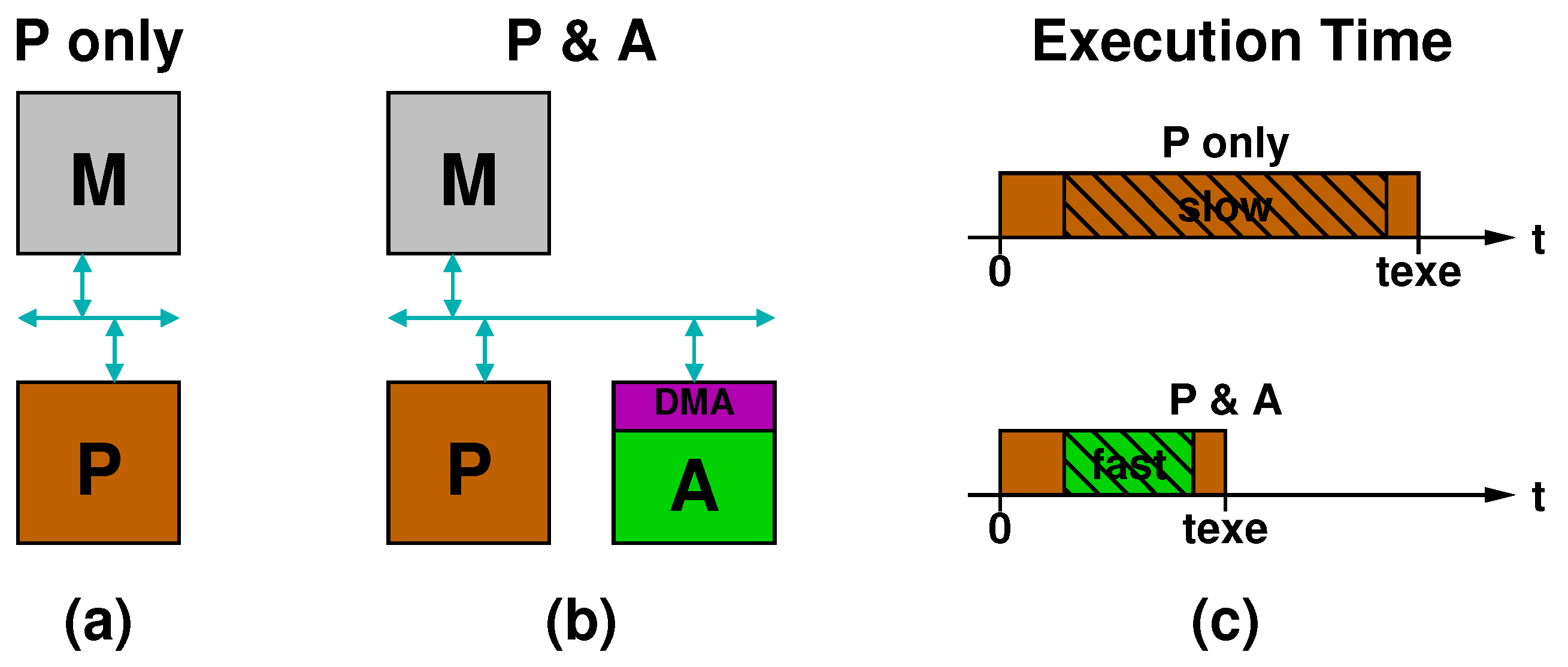
3.1. Speeding Computation Up With a Specialized Accelerator

Figure 4a,b illustrates two different implementations of the yellow processing block of Figure 1. In Figure 4a, labeled “P only”, a processor (P) communicates with the memory (M) through a bus. In Figure 4b, labeled “P & A”, an accelerator (A) is also connected to the bus and accesses the memory via DMA. Figure 4c sketches the timing diagrams of execution time for the two configurations. In the “P only” case, the processor runs from the beginning till the end (brown bar), while, in the “P & A” case, the accelerator is invoked at some point and runs for a certain amount of time (green bar) before handing over the execution again to the processor. Note that the initial and final parts of the execution time are the same in the two cases: in the “P & A” case the accelerator replaces the “slow” section of the code with a “fast one”.
The main reasons a specialized accelerator in the P & A case can be faster than a general purpose processor in the P-only case are: (i) the use of specialized arithmetic units; (ii) the higher level of computation parallelism; and (iii) the higher level of pipelining that can be achieved through a careful design. Another factor to consider is the clock frequency. Especially in the case of a programmable SoC on FPGA, where the processor is often a fixed hardwired component, whereas the accelerator is synthesized from register-transfer level (RTL) code and implemented in the programmable logic part of the SoC, the clock frequency of the accelerator is not as high as the processor one. Nevertheless, the accelerator can typically speed up the computation thanks to the higher parallelism and pipelining and the use of specialized units.
A last factor to consider is the speed of data communication, which basically boils down to evaluating how fast the accelerator can access the data stored in memory. Clearly, if the data transfer time alone in the P & A case exceeds by far the time spent by the processor for the computation in the P-only case, there is no point in using the accelerator. When data transfer time and computation time are comparable, a way to hide the latency of data communication consists in overlapping data transfer and data processing.
We return to these important design aspects below after the description of the hardware platform in which we implemented our processing system.

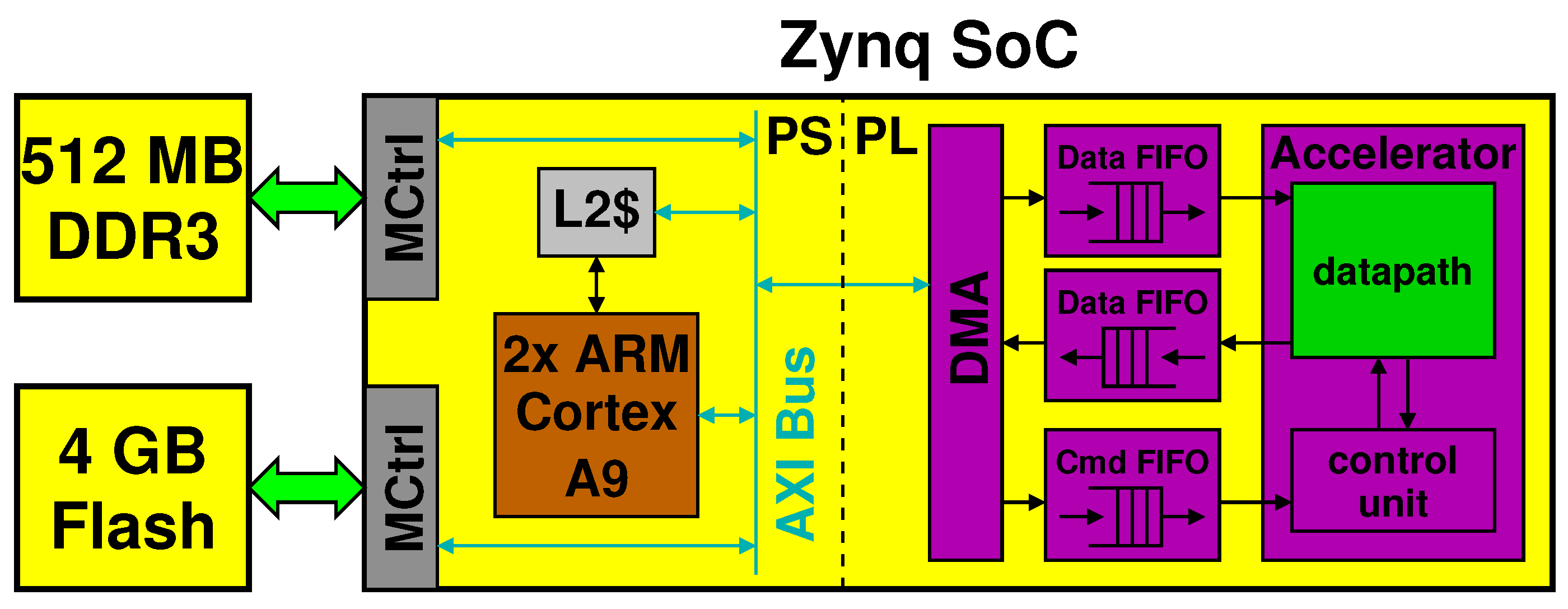
3.2. Hardware Platform

The processing block in yellow in Figure 1 is mapped to an embedded system consisting of a Xilinx Zynq programmable SoC with external memory (DDR3 and NAND Flash) and standard peripherals for connectivity (WiFi, USB) and display (HDMI, VGA). For development and testing, we used the Digilent Zedboard, a low-cost board that contains a Zynq XC7Z020, 512-MB low power DDR3 DRAM memory, 4-GB flash in a removable SD card, as well as the mentioned peripherals. We let a version of Linux run on the Zynq, based upon Ubuntu LTS 16.04 for ARM [12].
The Zynq SoC chip is split in two parts. In the Processing System (PS) part, the Zynq sports primarily a dual-core ARM Cortex A9 with its own L1 and L2 cache. In the Programmable Logic (PL) part, it features an Artix-7 Xilinx FPGA.
Figure 5 shows the processing block and highlights the connections between the PS and PL parts through an AXI bus. It also shows a hypothetical accelerator implemented in the PL part, which communicates with the PS by means of FIFOs and of a direct memory access (DMA) controller.
In the pseudo-code in Algorithm 1, we can identify two main sections: the computation of the SVD (line 1) and computation associated with the for loop (Lines 7–12). The other parts are irrelevant from the computational point of view. The computation of the SVD, however, can be done offline and the results stored in the SD card, so that they can be retrieved from there sufficiently quickly before executing the rest of the code. Therefore, we designed an accelerator to speed up the computation of the for loop.

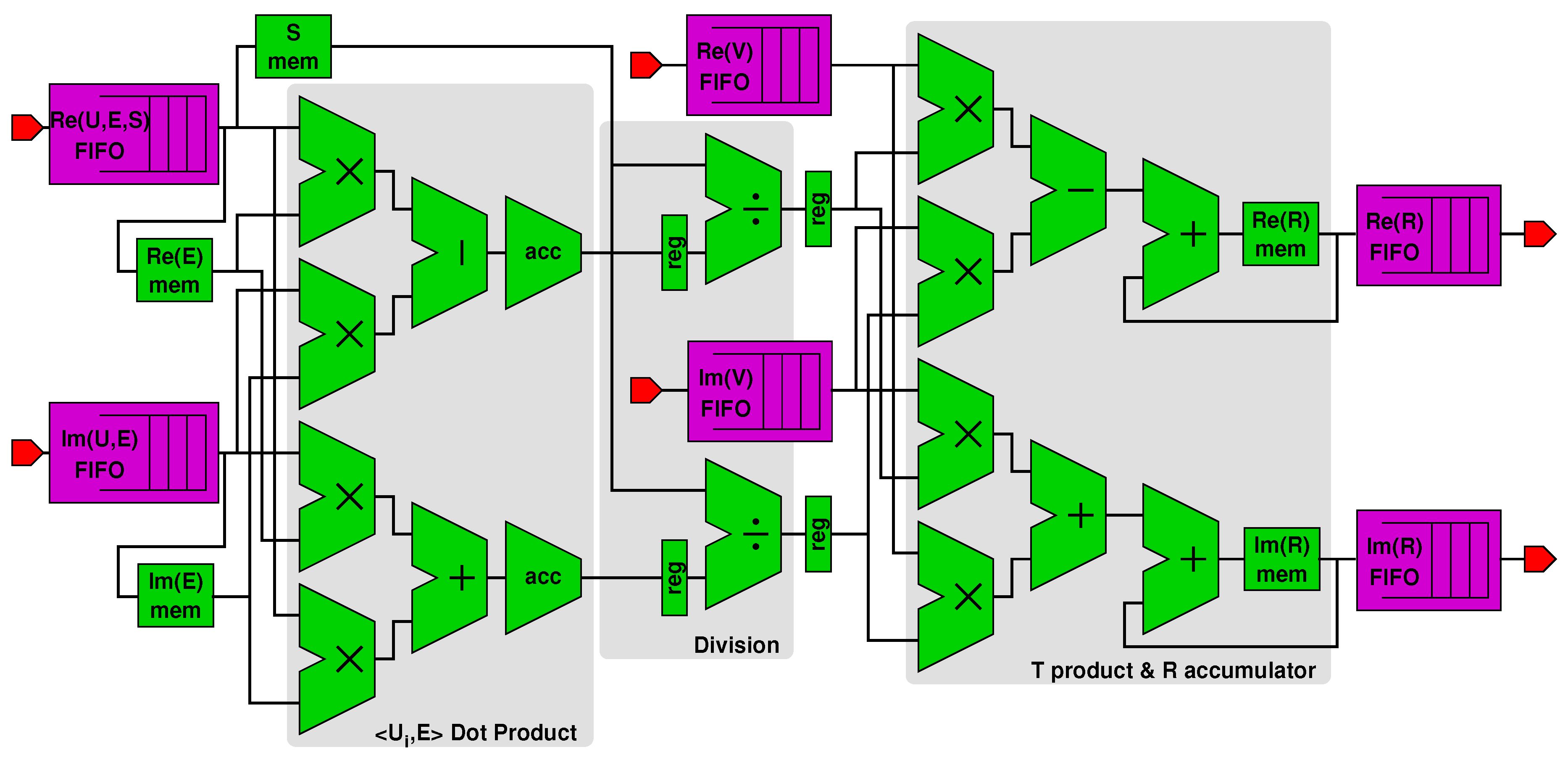
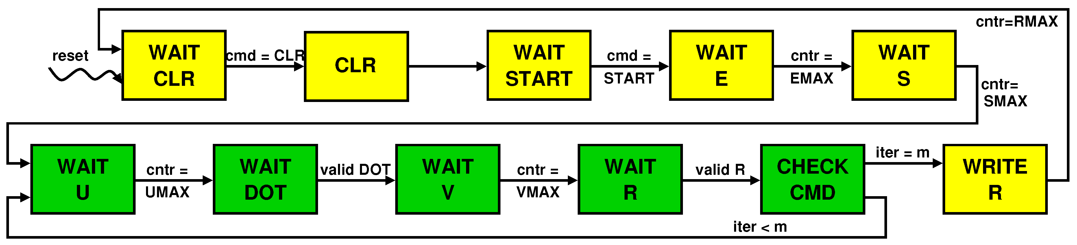
3.3. Accelerator Design

One of the challenges in this accelerator design is the need for floating-point (FP) computation to keep the same precision of the software implementation. The design complexity is reduced to a certain extent thanks to the various pre-designed FP blocks available in the Xilinx Vivado design tool, e.g., multipliers, adders, dividers, etc. These blocks support the AXI stream protocol, which simplifies their composition. They are also fully pipelined, which makes them interesting for our acceleration application in which input data arrays (primarily U and V ) are streamed at high speed via DMA and need to be processed right away.
We used such composable blocks to design the accelerator in Figure 5, which implements the functions corresponding to Lines 7–12 of Algorithm 1. Figure 6 is a detailed view of the accelerator’s datapath (the connections with the control unit are not shown for better clarity). The figure shows:
  • A first subblock computes the dot product x between complex vectors U i and E (fetched from an on-chip memory), resulting in variables Re ( x ) and Im ( x ) stored in proper registers (see Line 8 in Algorithm 1).
  • A second divider subblock computes Re ( y ) and Im ( y ) starting from Re ( x ) and Re ( y ) and from the singular value σ i (Line 9). The singular values are stored in and loaded from an on-chip memory within the PL part of the Zynq, as shown in figure.
  • A third subblock accumulates R values with the newly computed Re ( T ) and Im ( T ) (Lines 10–11). The values of R are also stored in their own on-chip memory.
As we previously pointed out, the accelerator leverages higher parallelism and deeper pipelining than the general purpose processor. In fact, both for the dot product x and the accumulation R , four FP multiplications are computed in parallel and are concurrent with various FP additions or subtractions thanks to pipelining. Moreover, the concurrency of control and datapath operation in the accelerator removes the control overhead for handling the loop in Algorithm 1, whereas the processor may incur such loop overheads.
Figure 5 also shows the data FIFOs used for the communication between the PS and the PL parts. In particular, two FIFOs are used for transferring first E and S arrays, which get stored in the respective on-chip memories shown in Figure 6, and then for transferring the columns of U . Two more FIFOs are used for transferring only the columns of V . Two FIFOs in the reverse direction are used for transferring back real and imaginary values of R .
The reason the same FIFOs are used to transfer real and imaginary parts of E , S , and U is because E and S can be transferred once and for all before the while loop in Algorithm 1, and then U ’s columns can be transferred one at a time at each loop iteration. Therefore, there would not be any advantage in using individual FIFOs for each of these arrays. Since each column of U is used only once per iteration, there is no need to store them in on-chip memory as it happens for E and S , which  instead get reused at every iteration.
The control unit in Figure 5 handles the repetition of the computation performed by the datapath according to the number of loop iterations m in Algorithm 1. This number is transferred to the control unit via the command FIFO prior to starting the data transfer of U and V columns. For each of these m iterations, the control unit reads data from the FIFOs and orchestrates the execution of the three subblocks in the datapath, as in Figure 6.
The control unit is a Finite State Machine (FSM) whose evolution is represented by the state transition diagram in Figure 7. The state change occurs based on explicit commands sent by the processor to the accelerator via the command FIFO (e.g., cmd = START and cmd = STOP) or on internal events, such as the terminal count raised after completion of reading E , S , U , and V from their FIFOs (e.g., cntr = UMAX) or flags indicating the completion and so the validity of the computation (e.g., valid DOT). Note that the green colored states belong to the loop that is repeated m times. The diagram clearly shows that E and S are transferred before the beginning of the loop so that their FIFOs can be reused for sending U values.
The pseudo-code in Algorithm 2 shows the code modifications with respect to Algorithm 1 that are required to support the accelerator. From the processor side, the workload consists primarily in controlling the data transfer from/to the external memory and from/to the accelerator. The actual computation is performed by the accelerator after it receives the “start” command (Line 10 of Algorithm 2).
Note that putdata and putcmd operations are non-blocking, therefore the two columns U i and V i are streamed simultaneously. Moreover, the control unit lets the datapath start as soon as the first data are available at the output of the FIFOs, hence enabling a complete overlap of data transfer and computation.
Algorithm 2 Pseudo-code of the hardware-accelerated implementation
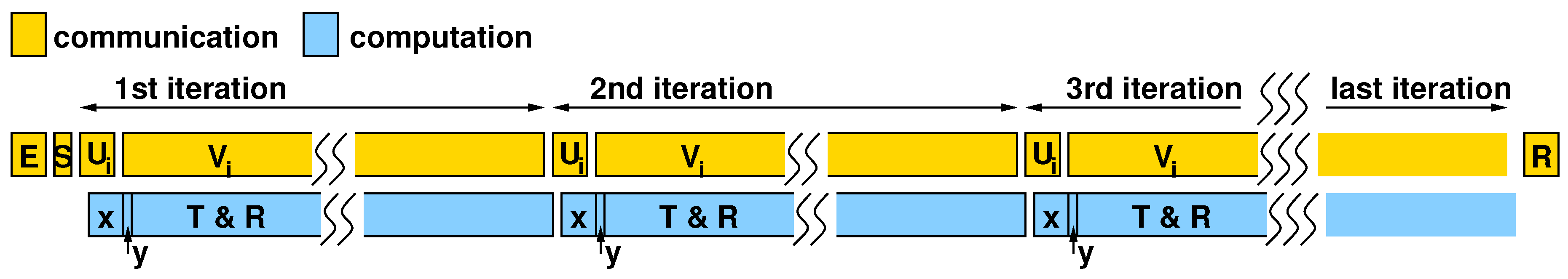
 1:
( U , S , V ) = SVD ( L ) ;     ▹ Singular Value Decomposition of L operator, computed offline
 2:
putdata( S );                   ▹ S sent to the accelerator via FIFO data queue
 3:
E measured variation of scattered field
 4:
putdata( E );                  ▹ E sent to the accelerator via FIFO data queue
 5:
θ = θ min ;
 6:
while θ < θ max do
 7:
    m = index of singular value σ m S closer to θ ;
 8:
    putcmd(m);                ▹m sent to the accelerator via FIFO command queue
 9:
    putcmd(reset( R ));           ▹ “reset R ” command sent via FIFO command queue
10:
    putcmd(start);              ▹ “start” command sent via FIFO command queue
11:
    for i = 1 to m do
12:
        putdata( U i );                 ▹ith column of U sent via FIFO data queue
13:
        putdata( V i );                 ▹ith column of V sent via FIFO data queue
14:
    end for
15:
    getdata( R );                      ▹ R retrieved from FIFO data queue
16:
    storage R ;                        ▹ R stored in flash SD memory
17:
     θ = θ + Δ ;
18:
end while

4. Results

We designed the accelerator and its FIFO interfaces at register-transfer level (RTL) using VHDL hardware description language and implemented it with Vivado 2016.1, which performs logic synthesis and place and route targeting the FPGA of the XC7Z020 Zynq device. The accelerator uses a single clock running at 100 MHz. The utilization of the various FPGA resources is reported in Table 3.
Note that the accelerator uses less than 20% of the logic resources—look-up tables (LUTs), flip-flops (FFs), and digital signal processing blocks (DSPs). The Block RAMs (BRAMs) saturate the utilization limit because all the FIFOs use this type of resource: 70% of BRAM resources are used by FIFOs, whereas the accelerator uses the remaining 30% to store E , S , and R .
Since computation and communication overlap, as shown in the sketched timing diagram in Figure 8, the overall execution time is determined by the data-transfer time from the processor to the accelerator and back. The total time is primarily determined by the time to transfer the columns of U and V at each iteration of the for loop, given that the E , S , and R are transferred only once.
The AXI bus clock is 100 MHz and one floating point value can be transferred at each bus clock cycle in burst mode. As a result, columns of U and V are transferred each in 1152/100 = 11.52 µs and 37380/100 = 373.8 µs, respectively. Typical number of iterations for the for loop are around 300 for thresholds between −80 and −50 dB, while this value tends to decrease for higher threshold values, as shown in Figure 9a.
The corresponding total execution time is shown in Figure 9b where the blue and red curves represent the software case in the ARM processor and the hardware-accelerated case, respectively. A 5× improvement is observed when the accelerator is used. The purple curve represents instead the software case for an Intel Xeon Processor E5-2650. Notice that there is a significant performance gap between our accelerator and the powerful Xeon CPU (7× less speed). This performance advantage is obtained, however, at a significant power cost because the Xeon power consumption is on the order of 100 W.
The board where we implemented our processing system consumes instead only 3.8 W, i.e., around 26 times less. Therefore, the performance-per-watt figure of merit of our system is about 3.7× greater than that of the Xeon CPU. Unfortunately, the board allows us to measure only the overall power, which includes several other larger contributions than what the ARM processor and the accelerator actually consume. As a result, we were not able to separate the processor contribution from the accelerator one. Nevertheless, the order of magnitude is perfectly compatible with the requirements of low power and, as a consequence, also of of small form factor (no need for large heat sinks or power supply units).

5. Related Work

Research groups working on MI applied to the brain stroke have focused either on the development of specific MI algorithms and their numerical evaluation (e.g., [3,10,13,14,15]), or on the implementation of prototype systems (e.g., [8,16,17,18,19,20]).
Due to the similarity between MI applied to breast cancer detection and to brain stroke monitoring, we believe that some of the concepts, methods, and designs developed for the former application will hold for the latter. In particular, thanks to the availability of commercial off-the-shelf components in the RF bandwidths used for these applications, we are confident that it is possible to keep low the cost of these MI systems, as shown in References [5,6,7].
The approach described in this paper has commonalities in particular with the work in Reference [6]. Even if the biomedical application is different, a Xilinx Zynq SoC is used to accelerate an MI algorithm in both works. The imaging algorithm used in the present work, however, is significantly different and is based on the TSVD approach rather than on the Interferometric MUSIC algorithm [21]. This means that signals are acquired at a single frequency rather than in time domain or at multiple frequencies, which simplifies both the acquisition and the processing. The computation is also simpler because there is no need to compute the propagation Green functions, which require the hardware implementation of non-trivial functions (e.g., exponential).
To the best of our knowledge, this is the first work to address the problem of accelerating an MI algorithm applied to brain stroke detection or monitoring. This is because the application of microwaves to this medical imaging problem is relatively new. There have been previous works, however, on accelerating MI algorithms, especially for breast cancer detection. In [22], the authors proposed accelerating the MI algorithms on a Cell broadband engine processor. In [23,24], the researchers suggested GPU acceleration. A GPU accelerator may not the best implementation choice for power-constrained or form-factor limited embedded systems. An accelerator implemented in FPGA or ASIC technology is in general more appropriate for these scenarios [25,26,27].
In general, MI applications do not escape the rule for which increase of performance and reduction of power and cost need more customization. Domain-specific computing architectures are the appropriate response to a call for ever increasing computing needs with power limitations. This is well exemplified, for instance, in Reference [28], which shows how several medical imaging applications can benefit from a domain-specific FPGA platform architecture. Another key medical imaging application where FPGAs help reduce cost and power is ultrasound, as shown by References [29,30]. Our work confirms this general trend.

6. Conclusions

In this paper, we describe the design of a low-cost low-power processing subsystem used in a microwave imaging system for brain stroke monitoring. The processing subsystem consists primarily of a Xilinx Zynq SoC device, which features an ARM-based CPU as well as an FPGA connected with the CPU through AXI bus interfaces. By implementing in the FPGA a hardware accelerator in charge of executing the heavy part of the computation, we obtain a 5× acceleration of the imaging code without losing precision with respect to full software execution.

Author Contributions

All authors contributed substantially to the paper. Conceptualization, I.S., G.T., and M.R.C.; Software, I.S., G.T., J.A.T., and R.S.; Hardware, I.S. and M.R.C.; Validation, I.S. and G.T.; Writing—Original Draft Preparation, I.S., G.T. and M.R.C; Writing—Review and Editing, M.R.C. and F.V.; Supervision, M.R.C., F.V., and L.C.; Project Administration, F.V.; and Funding Acquisition, F.V. and L.C.

Funding

This work was supported by the Italian Ministry of University and Research (MIUR) under the PRIN project “MiBraScan–Microwave Brain Scanner for Cerebrovascular Diseases Monitoring” and by the Compagnia di San Paolo under the project “MIT-Food, Microwave Imaging Technology for Food Contamination Monitoring”.

Conflicts of Interest

The authors declare no conflict of interest. The founding sponsors had no role in the design of the study; in the collection, analyses, or interpretation of data; in the writing of the manuscript, and in the decision to publish the results.

Abbreviations

The following abbreviations are used in this manuscript:
MIMicrowave Imaging
SVDSingular Value Decomposition
TSVDTruncated SVD
FPGAField Programmable Gate Array
PSoCProgrammable System-on-Chip
CPUCentral Processing Unit
DMADirect Memory Access
FPFloating Point
PSProcessing System
PLProgrammable Logic
FIFOFirst-in First-out

References

  1. Mackay, J.; Mensah, G. The Atlas of Heart Disease and Stroke; World Health Organization: Geneve, Switzerland, 2004. [Google Scholar]
  2. Meaney, P. Microwave Imaging and Emerging Applications. Int. J. Biomed. Imaging 2012. [Google Scholar] [CrossRef] [PubMed]
  3. Semenov, S.Y.; Corfield, D.R. Microwave Tomography for Brain Imaging: Feasibility Assessment for Stroke Detection. Int. J. Antennas Propag. 2008. [Google Scholar] [CrossRef]
  4. Nikolova, N.K. Microwave Imaging for Breast Cancer. IEEE Microw. Mag. 2011, 12, 78–94. [Google Scholar] [CrossRef]
  5. Zeng, X.; Fhager, A.; He, Z.; Persson, M.; Linner, P.; Zirath, H. Development of a Time Domain Microwave System for Medical Diagnostics. IEEE Trans. Instrum. Meas. 2014, 63, 2931–2939. [Google Scholar] [CrossRef]
  6. Pagliari, D.J.; Pulimeno, A.; Vacca, M.; Tobon, J.A.; Vipiana, F.; Casu, M.R.; Solimene, R.; Carloni, L.P. A low-cost, fast, and accurate microwave imaging system for breast cancer detection. In Proceedings of the 2015 IEEE Biomedical Circuits and Systems Conference (BioCAS), Atlanta, GA, USA, 22–24 October 2015; pp. 1–4. [Google Scholar] [CrossRef]
  7. Casu, M.R.; Vacca, M.; Tobon, J.A.; Pulimeno, A.; Sarwar, I.; Solimene, R.; Vipiana, F. A COTS-Based Microwave Imaging System for Breast-Cancer Detection. IEEE Trans. Biomed. Circ. Syst. 2017, 11, 804–814. [Google Scholar] [CrossRef] [PubMed] [Green Version]
  8. Persson, M.; Fhager, A.; Trefná, H.D.; Yu, Y.; McKelvey, T.; Pegenius, G.; Karlsson, J.; Elam, M. Microwave-Based Stroke Diagnosis Making Global Prehospital Thrombolytic Treatment Possible. IEEE Trans. Biomed. Eng. 2014, 61, 2806–2817. [Google Scholar] [CrossRef] [PubMed] [Green Version]
  9. Bertero, M.; Boccacci, P. Introduction to Inverse Problems in Imaging; CRC Press: Bristol, UK, 1998. [Google Scholar]
  10. Scapaticci, R.; Bucci, O.M.; Catapano, I.; Crocco, L. Differential Microwave Imaging for Brain Stroke Followup. Int. J. Antennas Propag. 2014. [Google Scholar] [CrossRef]
  11. Eigen. Available online: http://eigen.tuxfamily.org (accessed on 26 September 2018).
  12. Xillinux. Available online: http://xillybus.com/xillinux (accessed on 26 September 2018).
  13. Vasquez, J.A.T.; Scapaticci, R.; Turvani, G.; Vacca, M.; Sarwar, I.; Casu, M.R.; Dassano, G.; Joachimowicz, N.; Duchěne, B.; Bellizzi, G.; et al. A feasibility study for cerebrovascular diseases monitoring via microwave imaging. In Proceedings of the 2017 International Conference on Electromagnetics in Advanced Applications (ICEAA), Verona, Italy, 11–15 September 2017; pp. 1280–1282. [Google Scholar] [CrossRef]
  14. Stevanovic, M.N.; Scapaticci, R.; Crocco, L. Brain stroke monitoring using compressive sensing and higher order basis functions. In Proceedings of the 2017 11th European Conference on Antennas and Propagation (EUCAP), Paris, France, 19–24 March 2017; pp. 2742–2745. [Google Scholar] [CrossRef]
  15. Bisio, I.; Estatico, C.; Fedeli, A.; Lavagetto, F.; Pastorino, M.; Randazzo, A.; Sciarrone, A. Brain Stroke Microwave Imaging by Means of a Newton-Conjugate-Gradient Method in Lp Banach Spaces. IEEE Trans. Microw. Theory Tech. 2018, 66, 3668–3682. [Google Scholar] [CrossRef]
  16. Mohammed, B.J.; Abbosh, A.M.; Mustafa, S.; Ireland, D. Microwave System for Head Imaging. IEEE Trans. Instrum. Meas. 2014, 63, 117–123. [Google Scholar] [CrossRef]
  17. Mobashsher, A.T.; Abbosh, A.M.; Wang, Y. Microwave System to Detect Traumatic Brain Injuries Using Compact Unidirectional Antenna and Wideband Transceiver With Verification on Realistic Head Phantom. IEEE Trans. Microw. Theory Tech. 2014, 62, 1826–1836. [Google Scholar] [CrossRef]
  18. Bashri, M.S.R.; Arslan, T. Low-cost and compact RF switching system for wearable microwave head imaging with performance verification on artificial head phantom. IET Microw. Antennas Propag. 2018, 12, 706–711. [Google Scholar] [CrossRef] [Green Version]
  19. Scapaticci, R.; Donato, L.D.; Catapano, I.; Crocco, L. A Feasibility Study on Microwave Imaging for Brain Stroke Monitoring. Prog. Electromagn. Res. Boke Monit. 2012, 40. [Google Scholar] [CrossRef]
  20. Scapaticci, R.; Tobon, J.; Bellizzi, G.; Vipiana, F.; Crocco, L. A Feasibility Study on Microwave Imaging for Brain Stroke Monitoring. IEEE Trans. Antennas Propag. 2018. [Google Scholar] [CrossRef]
  21. Ruvio, G.; Solimene, R.; Cuccaro, A.; Ammann, M.J. Comparison of Noncoherent Linear Breast Cancer Detection Algorithms Applied to a 2-D Numerical Model. IEEE Antennas Wirel. Propag. Lett. 2013, 12, 853–856. [Google Scholar] [CrossRef]
  22. Xu, M.; Thulasiraman, P.; Noghanian, S. Microwave tomography for breast cancer detection on Cell broadband engine processors. J. Parallel Distrib. Comput. 2012, 72, 1106–1116. [Google Scholar] [CrossRef]
  23. Shahzad, A.; O’Halloran, M.; Glavin, M.; Jones, E. A novel optimized parallelization strategy to accelerate microwave tomography for breast cancer screening. In Proceedings of the 2014 36th Annual International Conference of the IEEE Engineering in Medicine and Biology Society, Chicago, IL, USA, 26–30 August 2014; pp. 2456–2459. [Google Scholar]
  24. Elahi, M.; Shahzad, A.; Glavin, M.; Jones, E.; O’Halloran, M. GPU accelerated Confocal microwave imaging algorithms for breast cancer detection. In Proceedings of the 2015 9th European Conference on Antennas and Propagation (EuCAP), Lisbon, Portugal, 13–17 April 2015; pp. 1–2. [Google Scholar]
  25. Casu, M.R.; Colonna, F.; Crepaldi, M.; Demarchi, D.; Graziano, M.; Zamboni, M. UWB Microwave Imaging for Breast Cancer Detection: Many-core, GPU, or FPGA? ACM Trans. Embed. Comput. Syst. 2014, 13, 109:1–109:22. [Google Scholar] [CrossRef]
  26. Pagliari, D.J.; Casu, M.R.; Carloni, L.P. Acceleration of microwave imaging algorithms for breast cancer detection via High-Level Synthesis. In Proceedings of the 2015 33rd IEEE International Conference on Computer Design (ICCD), New York, NY, USA, 18–21 October 2015; pp. 475–478. [Google Scholar] [CrossRef]
  27. Pagliari, D.J.; Casu, M.R.; Carloni, L.P. Accelerators for Breast Cancer Detection. ACM Trans. Embed. Comput. Syst. 2017, 16, 80:1–80:25. [Google Scholar] [CrossRef]
  28. Cong, J. Customizable domain-specific computing. IEEE Des. Test Comput. 2011, 28, 6–15. [Google Scholar] [CrossRef]
  29. Amaro, J.; Yiu, B.Y.S.; Falcao, G.; Gomes, M.A.C.; Yu, A.C.H. Software-based high-level synthesis design of FPGA beamformers for synthetic aperture imaging. IEEE Trans. Ultrason. Ferroelectr. Freq. Control 2015, 62, 862–870. [Google Scholar] [CrossRef] [PubMed]
  30. Ibrahim, A.; Hager, P.A.; Bartolini, A.; Angiolini, F.; Arditi, M.; Thiran, J.; Benini, L.; Micheli, G.D. Efficient Sample Delay Calculation for 2-D and 3-D Ultrasound Imaging. IEEE Trans. Biomed. Circ. Syst. 2017, 11, 815–831. [Google Scholar] [CrossRef] [PubMed] [Green Version]
Figure 1. Hardware systems composed of a helmet with 24 antennas, a switch matrix for the routing of Tx/Rx RF signals, and the processing unit for the image elaboration.
Jlpea 08 00043 g001
Figure 2. Example of reconstructed images obtained with a threshold value of −80 dB.
Jlpea 08 00043 g002
Figure 3. Example of reconstructed images obtained with a threshold value of −20 dB.
Jlpea 08 00043 g003
Figure 4. Comparison between processing systems implemented: as a general purpose processor alone (a); or with an accelerator (b); and related timing diagrams (c).
Jlpea 08 00043 g004
Figure 5. Detail of the processing system implemented in a Xilinx Zynq SoC.
Jlpea 08 00043 g005
Figure 6. Datapath of the accelerator.
Jlpea 08 00043 g006
Figure 7. State transition diagram for the finite state machine that controls the accelerator’s datapath.
Jlpea 08 00043 g007
Figure 8. Timing diagram showing concurrency of communication (between processor and accelerator) and computation (within the accelerator).
Jlpea 08 00043 g008
Figure 9. (a) Number of iterations; and (b) execution time.
Jlpea 08 00043 g009
Table 1. Algorithm parameters.
ParameterValueNote
NV24Number of transmitter antennas
NM24Number of receiver antennas
NC18,690Total grid points in 3D volume
θ min −80 dBMinimum threshold
θ max −10 dBMaximum threshold
Δ 10 dBThreshold step
Table 2. Data type and dimensions.
DataTypeSize (FP)
E Complex Vector 2 × N M 2 = 1152
S Real Vector N M × N V = 576
U Complex Matrix ( 2 × N M 2 , 2 × N M 2 ) = ( 1152 , 1152 )
V Complex Matrix ( 2 × N C , 2 × N M 2 ) = (37,380,1152)
R Complex Vector 2 × N C = 37 , 380
Table 3. FPGA resources utilized by the accelerator in the Xilinx XC7Z020 Zynq device.
ResourceUtilization
LUTs19.04%
FFs14.2%
BRAM100%
DSPs14.55%
IOBs38%

