Article

Ray Tracing Modeling of Electromagnetic Propagation for On-Chip Wireless Optical Communications

1
Department of Electrical, Electronic and Information Eng. “G. Marconi”, University of Bologna, 40136 Bologna, Italy
2
Department of Engineering, University of Ferrara, 44122 Ferrara, Italy
3
Department of Electrical and Information Engineering, Polytechnic of Bari, 70126 Bari, Italy
*
Author to whom correspondence should be addressed.
J. Low Power Electron. Appl. 2018, 8(4), 39; https://doi.org/10.3390/jlpea8040039
Submission received: 13 September 2018 / Revised: 11 October 2018 / Accepted: 12 October 2018 / Published: 17 October 2018
(This article belongs to the Special Issue Emerging Interconnection Networks Across Scales)

Abstract

:
Multi-core processors are likely to be a point of no return to meet the unending demand for increasing computational power. Nevertheless, the physical interconnection of many cores might currently represent the bottleneck toward kilo-core architectures. Optical wireless networks on-chip are therefore being considered as promising solutions to overcome the technological limits of wired interconnects. In this work, the spatial properties of the on-chip wireless channel are investigated through a ray tracing approach applied to a layered representation of the chip structure, highlighting the relationship between path loss, antenna positions and radiation properties.

1. Introduction

The computation hunger affecting technological progress has fostered the development of multi-core architectures, where data processing is simultaneously carried out by several processors (or cores) embedded in the same processor die, thus dramatically reducing the computational effort. Since mutual interactions among the cores are necessary, they must be effectively interconnected. To this aim, traditional bus architectures have been replaced by networks on chip (NoC), where the processor chip includes electrical wires and routers besides cores and cache banks [1,2]. Nonetheless, interconnect issues such as layout complexity, high latency, and power consumption are far from being completely solved, to the extent that they might seriously thwart further evolution towards kilo-core architectures [3]. In particular, electrical wires undergo propagation delays and losses which do not scale down at the same rate as transistors, and they can hardly support the high data-rate required by core-to-core communications [2,4].
These issues can be partly tackled by optical networks on chip (ONoC) [4,5], which take advantage of optical interconnects to provide high-speed communications (also exploiting wavelength division multiplexing) with lower propagation delays and weaker propagation losses. Nonetheless, on-chip integration of optical sources still undergoes several technological limitations [5], e.g., related to the laser efficiency, which reduces as the chip temperature rises up and is in general quite low. On the other hand, off-chip lasers are more efficient but their coupling to the chip introduces additional losses [4] and poses additional issues related to the mechanical interconnection between the source and the die. Furthermore, important optical devices like micro-rings require extra-power expenditure to compensate for the resonant wavelength shift due to manufacturing geometric inaccuracies [4]. Finally, interfacing the optical network with the electrical circuitry of the cores entails some electro-optical conversion with negative effects on both energy loss/consumption and networking delays [4]. It is also worth mentioning that both electrical and optical NoC may suffer from unwanted and unpredictable cross-talk effects (especially at waveguide crossing and switching stages), which are expected to be harsher as the number of cores increases and the network layout becomes more complex. Three-dimensional circuit integration may space out interconnections, thus alleviating the cross-talk risk, but complicating the manufacturing process.
In this framework, wireless networks on-chip (WiNoC) have therefore attracted increasing consideration [1,3,6] as an effective solution to provide low-latency communications and to get rid of the interconnect routing and layout complexity when a large number of cores must be arranged into the processor integrated circuit (IC) [3]. Because of the current limitations on antenna technologies, WiNoC are often investigated up to the millimeter/sub-THz bands, where on-chip antenna integration may still represent a challenge and propagation is likely to occur in near field, and possible mutual coupling might therefore arise reducing the communication efficiency [7].
Therefore, optical wireless networks on chip (OWiNoC) have been recently proposed [8], aiming at preserving the main advantages of WiNoC (low latency, simpler network layout) but fostering far-field propagation and facilitating the antenna integration process. Moreover, relying on wireless optical communications can be particularly beneficial to envisage hybrid wired/wireless optical networks, because the same wavelength propagating on optical waveguides could be directly exploited for wireless connections without any further electro-optical conversion [8].
In spite of the existing studies carried out on WiNoC, quite little consideration has been seriously devoted to wireless channel modeling [5,9,10], and hardly ever at optical frequencies [11]. In this work, the OWiNoC propagation channel is specifically investigated by means of a ray tracing (RT) approach, which is expected to be quite reliable at so large frequencies and is also inherently fit to track the multipath nature of the on-chip wireless channel. In References [9,11], the analysis is basically limited to the frequency response of the channel, whereas prediction of the spatial field distribution limited to few wavelengths is provided in Reference [10]. Conversely, the primary goal of this study is the assessment of the far-field spatial fading (which is expected to be a serious impairment in the optical frequency range) and of the maximum communication distance for different chip structures. Moreover, the impact of the antenna position and radiation properties is here discussed to some extent in several reference cases, whereas oversimplified radiators in a single case study are considered in References [10,11].
The paper is organized as follows: Section 2 provides some general background about on-chip wireless propagation, whereas Section 3 deals with the physical structure of an IC and its representation as a multi-layered medium. The RT model for on-chip propagation analysis is presented in Section 4. Results of the RT simulations are discussed in Section 5, and some conclusions are finally drawn in Section 6.

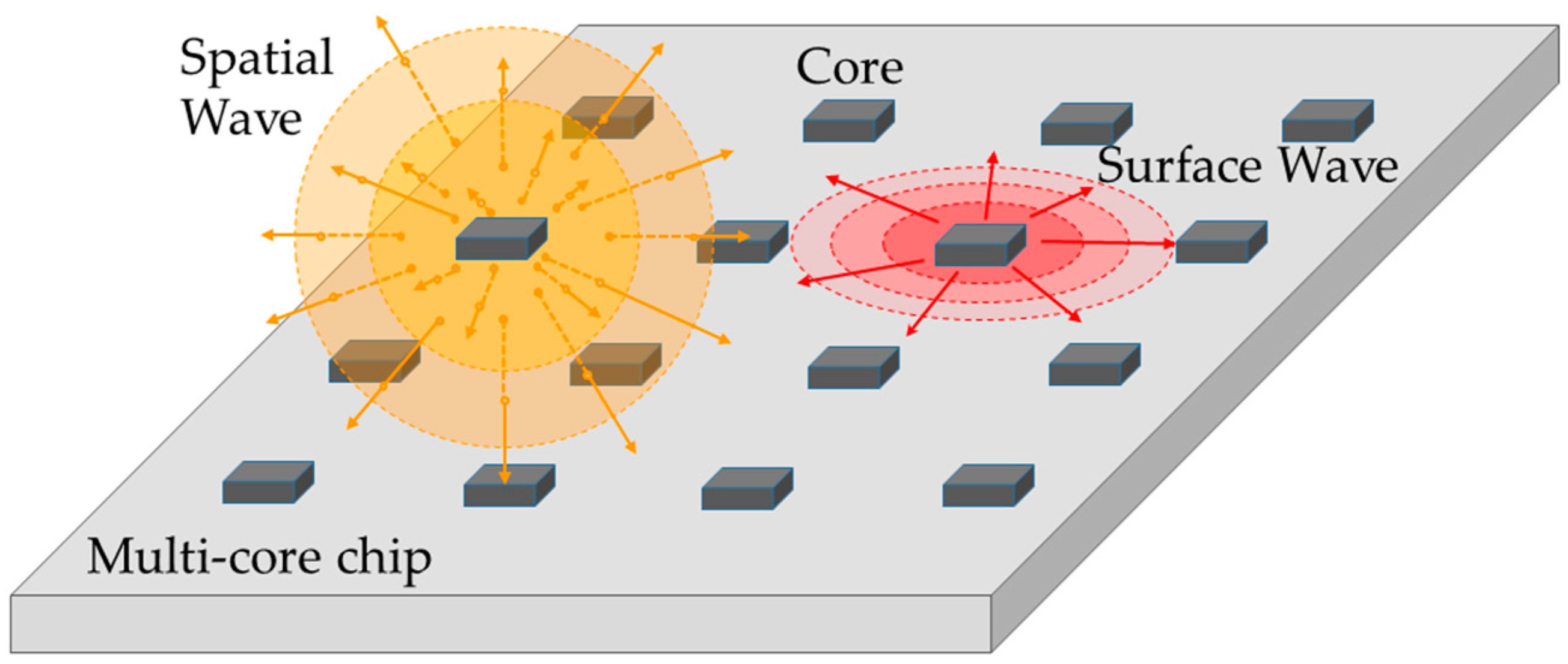
2. Background on Propagation Mechanisms and Optical WiNoC Requirements

Increasing the communication frequency in WiNoC can ease the antenna integration efforts, but also raises some propagation issues to be aware of. The communication range is always affected by the communication frequency, since greater isotropic attenuation is experienced at larger frequency as a general trend. In free space condition, the antenna gain can be easily related to the distance corresponding to the minimum required power at the receiver for a satisfactory communication by means of the Friis equation:
G = P R X , min P T X 4 π d λ  
where the same antennas are supposed at both link ends for the sake of simplicity, PRX,min and PTX are the receiver sensitivity and the overall transmitted power, respectively, d is the link distance and λ is the wavelength of the wireless signal in the propagation medium. For instance, an antenna gain equal to nearly 30 dB is needed to convey a power PRX,min = −25 dBm to the distance d = 1 mm under free space conditions and assuming PTX = 0 dBm and λ = 1 μm.
In spite of the tiny wavelength, the design of highly directive optical antennas is not a straightforward task, because the integration need poses serious constrains on the size of the on-chip devices. For instance, the plasmonic antennas proposed in References [8,12] exhibit a gain always lower than 10 dB, whereas it is increased to about 20 dB by the dielectric solution discussed in Reference [13], though at the expense of a quite larger antenna size. Owing to the current limitation on optical antenna gain, propagation conditions better than in free space would be therefore extremely beneficial to the optical wireless communications. Whether and to what extent this may occur in the on-chip wireless channel is investigated in the following sections. In this regard, surface electromagnetic waves are sometimes referred to as an effective means to improve propagation conditions compared to free space [2,14,15]. Although electromagnetic propagation is usually a three-dimensional phenomenon, i.e., spatial waves spring out of the transmitting antenna and spread over the full space interacting with the items all around, surface waves might be triggered under particular circumstances and travel close to the chip surface (and therefore in two spatial dimensions) between different cores (Figure 1). Since the surface wave is confined at the planar interface, its wavefronts undergo a smaller spatial broadening compared to a spatial wave, and therefore the corresponding path loss would increase proportionally to the link distance d instead of d2 as in free space [2].
In order to take full advantage of surface propagation, surface waves only should be excited. The launching efficiency of a surface wave is often defined as the ratio between the surface and the overall radiated power [16]. Design of effective surface wave antennas has been dealt with for quite a long time: investigations carried out on different surface wave launchers in Reference [17] pointed out that efficiency nearly equal to 100% could be easily achieved in theory, but not as much in practice. Moreover, theoretical analysis in the mm-wave band [10] highlighted that the role played by spatial/surface propagation is greatly affected by frequency, material properties, and position of the antennas within the on-chip wireless channel. Finally, surface wave interconnects represent a sort of emerging solution currently under investigation mainly at millimeter frequencies [2], and no significant studies have so far addressed design challenges for integrated surface wave launchers in the optical range.
Soothing the debate on whether optical WiNoC should better rely on spatial or surface propagation is far beyond the scope of this work. Here, possible surface propagation effects are simply neglected at the moment and the main goal is the investigation of the fading properties of the on-chip spatial radio channel.

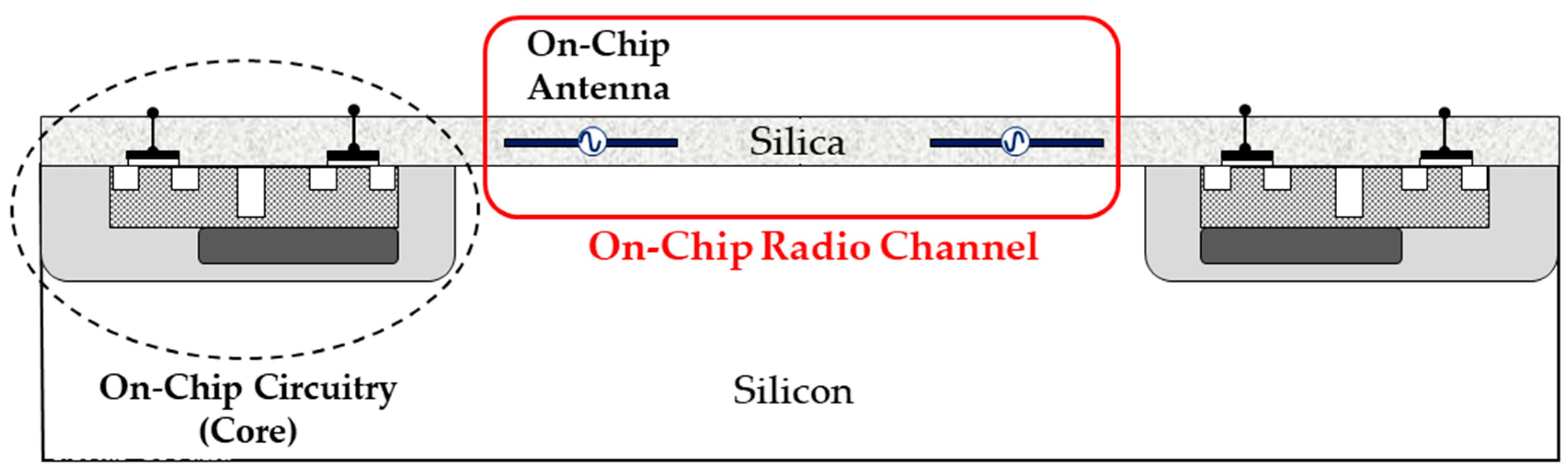
3. General Description of the Multi-Core Chip Structure

As a matter of fact, wireless propagation is quite sensitive to the properties of the environment where it takes place. Therefore, the first step for the electromagnetic characterization of the wireless channel always consists of its physical description. A very detailed and precise representation usually yields a deeper insight but is often limited to the specific case under investigation. Conversely, limiting the description of the scenario to the features mainly affecting electromagnetic propagation may result in prediction still reliable in many different cases, provided that they share the same macro structure. According to the latter approach, this section aims at identifying some common characteristics underlying any multi-core IC, in order to define some reference input layouts for the ray tracing propagation analysis carried out in Section 5.
With reference to the complementary metal-oxide semiconductor (CMOS) technology, an IC is always achieved from a silicon wafer, and is made of a silicon layer covered with a thinner film of silicon dioxide (or silica) in the first stage of manufacturing [18]. In spite of the further technological processes aimed at deploying the electronic circuitry (e.g., devices—like transistors—and interconnects) onto the wafer, the on-chip wireless channel is still often represented as the layered dielectric structure sketched in Figure 2 [19]. The transmitter (TX) and the receiver (RX) are assumed buried inside the SiO2 layer herein [11], but they could also lie on its top [9,10]. The upper medium above SiO2 might be air in the simplest case [10,11] or a different passivation material (e.g., silicon nitride) [20].
It is worth mentioning that a pattern of some metallization layers is often inserted within the dielectric region [18], either for the interconnection of the upper circuit elements or increasing the reliability of the manufacturing process. The metallization can extend over the whole chip area, i.e., it is not necessarily limited to the circuitry regions. Moreover, a ground plane between the silicon substrate and the insulating layer might be helpful to prevent unwanted electromagnetic interference between the antennas and the circuitry [20].
Finally, the presence of the package housing of the IC can be also taken into account through the introduction of further layers respectively below and above the silicon and the air/passivation slabs. Although packages can be made of several different materials (e.g., ceramic or plastic), the analysis is here limited to the plastic case for the sake of simplicity. Since the IC sometimes lies on a metal ground acting as heat spreader [21], the bottom layer can be set of plastic or metal as a further option.
In summary, the on-chip wireless channel is here sketched according to the following layered structures (Figure 3):
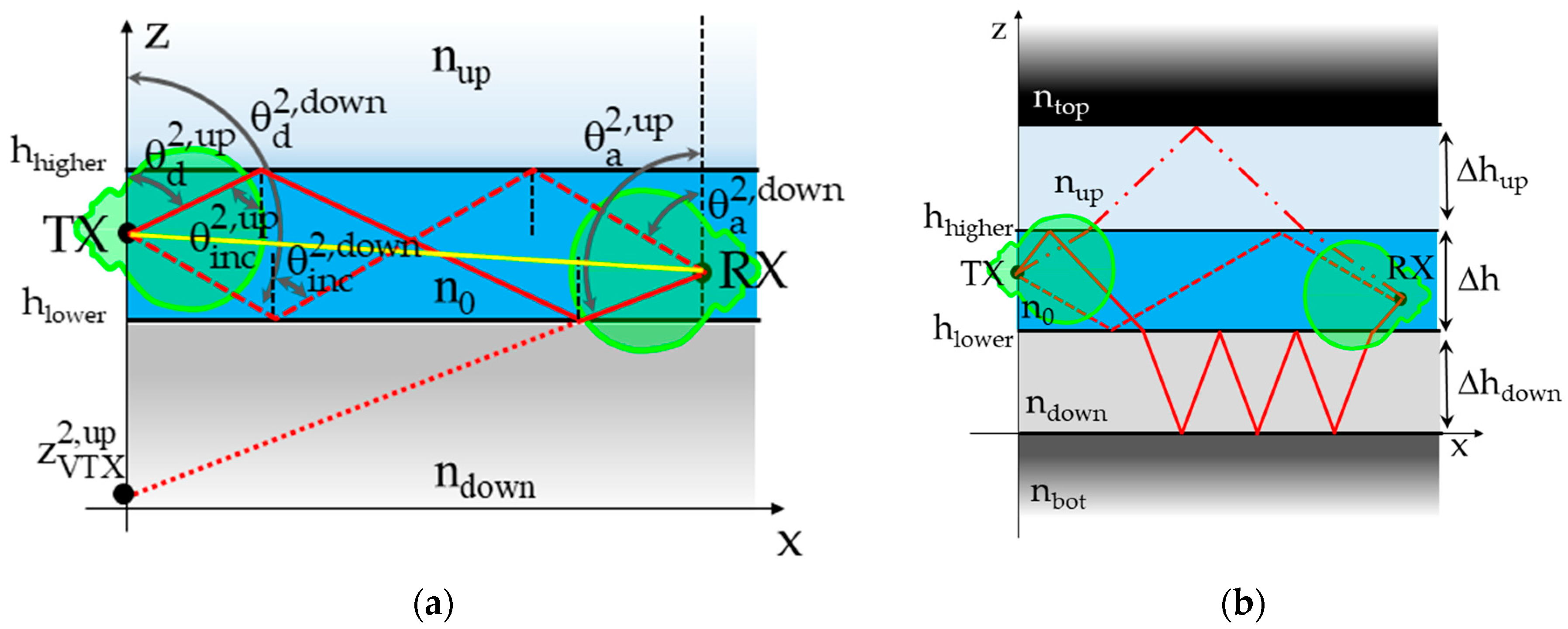
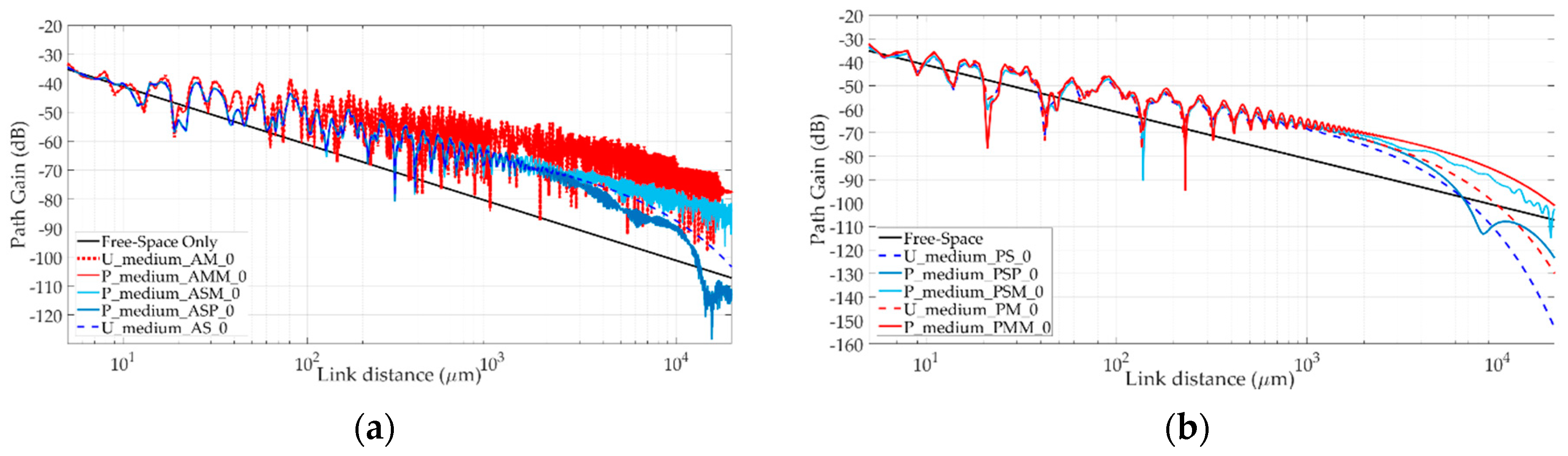
  • Unpacked, where a plane silica slab including the transmitting and the receiving antennas is bounded by two different media on the upper and on the lower side (Figure 3a). The upper region can be either air or a different passivation material, where the former case stands for possible situations with a refraction index in the superstrate lower than in the SiO2. The lower zone can be silicon or metal—in the latter case accounting for possible metallization layers inside the SiO2 or between the SiO2 and the Si regions.
  • Packed: where two additional layers are added at the bottom and on the top of the previous stack (Figure 3b). Either plastic or metal can be considered for the bottom region, whereas plastic is the only option for the top half-space.
Each interface between different media is supposed perfectly flat and infinitely wide at this stage of the investigation, so that spatial wave propagation consists of multiple reflections occurring in the vertical plane (xz in Figure 3). The electromagnetic properties of the materials are taken into account through their refraction indexes (n coefficients in Figure 3), whose reference values in the optical range are listed in Table 1 together with the thickness considered for the different layers. Real values are assumed for the refraction indexes (i.e., the lossy materials have not been considered so far).
Although the proposed layouts are rather simplified compared to a real IC structure, they are nonetheless expected to fit the need of providing a reliable insight into the main properties of on-chip propagation, which in the end is the primary goal of this study.

4. Ray Tracing Propagation Modeling in OWiNoC

Channel modeling for OWiNoC can effectively rely on RT simulators, whose accuracy is known to improve at large frequency as a general trend.
Furthermore, the description of the multi-core IC as a multi-layered structure with perfectly smooth, infinitely wide interfaces makes the ray tracing tasks easier, since the rays always lie in the same plane and the field computation turns out to be simpler compared to a non-layered structure, as explained in the following sub-sections for the unpacked and packed cases, respectively.

4.1. Unpacked Case

Wave propagation consists of multiple reflections occurring within the SiO2 slab, as sketched in Figure 4. Therefore, the electromagnetic field radiated to the RX after m bounces (m = 2 reflections are for instance shown in Figure 4a) can be expressed as:
E m = E 0 m e j β r m r m Π m ,        m 0  
being β = 2π/λ the wave number, rm the overall length of the ray, Πm the product of the m reflection coefficients, and E0m the TX antenna “emitted field” in the direction of departure of the ray. It is worth noting that Π0 = 1, since the direct ray undergoes no reflections. Moreover, the same reflection order m > 0 is always shared by a couple of rays (as sketched in Figure 4a), the former having the first reflection on the upper interface (and referred to as “up” in the following), the latter on the lower one (and identified by the label “down” herein).
It is worth mentioning that the path length rm can be regarded as the distance between the RX and an “mth virtual transmitter” (VTX), which is the “mirror” image of the TX (if m = 1) or of the (m − 1)th VTX (otherwise) with respect to the reflecting plane (image principle) [22]. For instance, the VTX associated with the double reflected “up-ray” is included in Figure 4a. According to the considered reference system, the following closed-form analytical expressions can be easily achieved for the VTXs locations in the unpacked case:
z V T X m , u p = { m    e v e n :     m ( h l o w e r h h i g h e r ) + z T X m    o d d :     ( m + 1 ) h h i g h e r ( m 1 ) h l o w e r z T X  
z V T X m , d o w n = { m    e v e n : m ( h h i g h e r h l o w e r ) + z T X m    o d d : ( m + 1 ) h l o w e r ( m 1 ) h h i g h e r z T X  
where zTX is the z-coordinate of the TX and hhigher and hlower are represented in Figure 3 and Figure 4a.
The evaluation of the Πm factor in Equation (2) requires the computation of the Fresnel reflection coefficients at the interfaces, and therefore of the angles of incidence of the rays ( θ i n c 2 , u p / d o w n in Figure 4a). By means of simple geometrical considerations, the incidence angles can be related to the positions of both the RX and the VTX as follows:
θ i n c m , u p / d o w n = a r c t g ( x R X | z R X z V T X m , u p / d o w n | )  
As a general rule, the larger the link distance (e.g., the xRX value) and/or the lower the number of undergone reflections, the “more grazing” the rays become, and therefore the greater the amount of reflected power. Since the reflection phenomenon also depends on the material properties (refraction index), the computation of Πm entails the assessment of the reflection coefficients at both the interfaces, which must be then properly multiplied taking into account the exact number of reflections occurring at the upper and at the lower boundaries. By definition, reflection coefficients always have an amplitude ≤1, meaning that depending on the materials and the incidence condition the power impinging on the upper and on the lower boundaries may be either constrained in the silica layer (total reflection) or leaked in the non-confined regions.
Finally, the emitted field is computed as:
E 0 m u p / d o w n = η P T X g T X ( θ d m , u p / d o w n ) 2 π n 0 p ^ T X ( θ d m , u p / d o w n ) e j β
where η = 120π, gTX( θ d m , u p / d o w n ) and p ^ T X ( θ d m , u p / d o w n ) are the transmitting antenna gain and polarization vector in the directions of departure of the up/down rays, respectively (as outlined in Figure 4a). The following formulas can be exploited for the computation of Equation (6):
θ d m , u p = θ i n c m , u p ,          θ d m , d o w n = π θ i n c m , d o w n  
Both the antenna gain pattern and the polarization vector in the propagation plane must be provided as input files to the RT engine; they may be indifferently achieved from numerical simulation of specific antenna layouts, or from simpler, ready-to-use analytical model representative of wider classes of antennas (e.g., isotropic, omnidirectional, directive, etc.).
Since the Fresnel reflection coefficients are available only for the transverse electric (TE) and magnetic (TM) polarizations (corresponding respectively to the ϕ ^ and θ ^ directions in the considered reference system), the polarization vector and therefore the emitted field must be decomposed into its TE and TM components, and the corresponding field components should be then independently evaluated according to Equation (2).
Once the rays have been tracked and the fields impinging on the RX have been computed, the overall received power can be achieved as [22]:
P R X = λ 2 8 π η | g R X ( θ a 0 ) [ p ^ R X ( θ a 0 ) · E 0 ] + m = 1 M r e f l g R X ( θ a m , u p ) [ p ^ R X ( θ a m , u p ) · E m u p ] + g R X ( θ a m , d o w n ) [ p ^ R X ( θ a m , d o w n ) · E m d o w n ] | 2  
being θa0 the direction of arrival at the RX of the direct field E 0 , θ a m , u p / d o w n the angle of arrival at the RX of the up/down rays after n reflections, Mrefl the maximum number of allowed bounces, gRX and p ^ R X are the antenna gain and the polarization vector of the receiving antenna. The angle of arrival can be computed as:
θ a m , u p / d o w n = { θ d m , u p / d o w n       ( m    e v e n ) π θ d m , u p / d o w n       ( m    o d d )  
Since Equations (2)–(10) represent a set of rather simple, closed-form expressions, rays tracking turns out to be quite fast, with computation time of few minutes for simulations accounting for a number of reflections up to some hundreds. Commercial RT tools would hardly be as much effective, because they are not specifically conceived for multi-layer scenarios, and therefore they have to rely on more general but also computationally heavier ray tracing algorithms. Besides, full wave models (e.g., Finite-Difference Time-Domain methods (FDTD)) are not even worthy of consideration, since they simply cannot handle far-field analysis in inhomogeneous media. Finally, the resort to modal representation of the field seems also not appropriate, because in spite of the layered structures here considered, propagation is however wireless and therefore not necessarily confined in one guiding layer, as shown and discussed in Section 5.

4.2. Packed Case

If the materials bounding the silica slab also have finite thickness, additional rays rise within the layered structure, which can still undergo multiple reflections inside a layer but also propagate among the different layers exploiting transmission at the interfaces (Figure 4b). Tracking such a huge multitude of rays would heavily increase the computational burden of the model, also because it would not simply consist of the closed-form, analytical formulas which hold in the Unpacked case.
In order to trade off prediction accuracy against computational effort, propagation above and below the SiO2 layer in the packed case is here heuristically modeled by means of the “total layer reflection coefficient” proposed in Reference [23]. As a ray sprung from the TX impinges on the upper/lower interface, it is partly reflected and partly transmitted beyond the boundary, where it triggers a multiple bounce mechanism. Each time the bouncing ray hits back the silica slab, transmission takes place, spilling some field into the SiO2 layer. All these contributions add up coherently in such a way that the total field resulting from the multiple bounce phenomenon can be expressed through the following “enhanced” reflection coefficient to be applied directly to the impinging ray (see Reference [23] for details):
Γ e n = Γ + T T i = 1 ( Ξ i Δ i Λ i Σ i )  
where the involved coefficients have the following meaning:
  • Γ is the standard Fresnel reflection coefficient at the interface;
  • Τ and Τ′ are the outward and the inward transmission coefficients at the silica slab boundaries;
  • Ξi is the product of the reflection coefficients related to the rays bouncing in the upper/lower layer;
  • Δi accounts for the phase shifts and propagation delays associated with the bouncing effect;
  • Λi and Σi take into account the attenuation experienced by the rays bouncing inside the layers, respectively associated with the possible material losses (actually not considered here, where lossless materials are supposed) and with the spatial spreading of the wavefronts. It is worth mentioning that Σi is actually not included in the original formula provided in Reference [23], and it has been here introduced to cope with the lack of respect for the plane wave and layer thinness conditions assumed in Reference [23].
In the end, propagation in the packed case can be modeled as for the unpacked case, provided that the Fresnel reflection coefficients are replaced by the enhanced formulation.

5. Simulation Results and Discussion

This section includes the outcomes of the RT model described in the previous section applied to the layered representations of the multi-core IC structure outlined in Section 3.

5.1. RT Input Data

In order to start the RT engine, the geometrical and electromagnetic description of both the propagation scenario (Table 1) and the TX/RX antenna characteristics must be provided as input data. The simulation frequency is 193.5 THz, corresponding to a wavelength of 1.55 μm (in vacuum) and therefore included in the conventional C-band for optical telecommunications. The emitted power by the TX is 0 dBm and the RX sensitivity has been set to −25 dBm, as reasonable detection threshold of the incoming signal. The maximum reflection order is set to 300 reflections, both on upper and lower layers.
As far as the antennas radiation properties are concerned, either an isotropic or a simple directive pattern has been supposed. The directive case consists of a simple single-lobe pattern always steered in the x direction (Figure 4). In particular, the radiation intensity is proportional to coskx), being αx < 90 deg. the angle between the direction of departure of the generic optical ray springing out from the Tx antenna and the x axis. The antenna gain G can be easily tuned through the k coefficient, according to the formula G = 2∙(k + 1). Since the rays always belong to the vertical plane, the RT simulator must be actually fed by a discrete representation of the radiation diagram in the xz plane, as sketched in Figure 5 for different G values. The polarization vector in the same plane must be also provided, in order to account for the polarimetric properties of the antenna. The same antennas with TE polarization are assumed at the link ends for the sake of simplicity, pointing toward each other’s (Figure 4).
Although analytical description of the antennas provides extreme flexibility, since as many radiation patterns as necessary can be easily achieved with negligible computation effort, any other radiation pattern—e.g., based on numerical simulation of specific antenna layout—can be investigated, provided that the required information is encoded in the correct format.
In order to distinguish the different possible cases, each simulation is labeled by means of an acronym encoded as follows:
  • Unpacked cases: U_Δstring_XY_GdB, where Δstring sets the width of the silica layer (possible values: “thin”, “medium”, “thick”, see Table 1), X and Y are characters identifying the top and the down media (X = “A”—Air—or “P”—Passivation, and Y = “S”—Silicon—or “M”—Metal) and GdB is the antennas gain value. For instance, the simulation carried out with isotropic radiators within a 10 μm SiO2 slab bounded by air and silicon at the upper and lower interfaces is referred to as “U_medium_AS_0”;
  • Packed cases: P_Δstring_XYZ_GdB, where Δstring, X, Y and GdB keep their meaning and Z is a further character setting the material for the bottom layer (possible values: “P”—Plastic—or “M”—metal). Therefore, adding a plastic package to the previous example would correspond to the label “P_medium_ASP_0”.

5.2. RT Simulation Results

Several RT simulations have been run aiming at the computation of the link Path Gain (PG) under different simulation conditions. Path gain is defined as the ratio between the power captured by the receiving antenna and the power radiated by the transmitting one [22]. It therefore represents the reciprocal (the opposite, in dB unit) of the propagation losses, i.e., of the attenuation experienced by the optical wireless signal as it propagates from the transmitting to the receiving antenna. Other losses may further impair the communication (e.g., coupling losses occurring within the circuits), but they are not considered in this study.
PG is plotted versus the link distance (μm) in Figure 6, for different materials combinations in the unpacked case and assuming isotropic radiators. The TX and the RX are placed in the middle of the SiO2 slab with medium thickness. The free space power is also drawn (black straight line), as reference. Two “breakpoints” can be highlighted as a general trend, the former corresponding to the distance where the PG rises up from the free-space line (rise point—Pr), the latter representing the farther distance where the PG drops below the free space curve (fall point—Pf). Three zones can be identified accordingly:
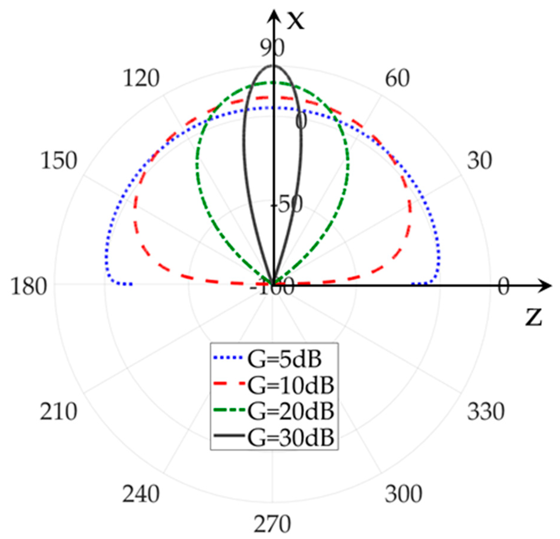
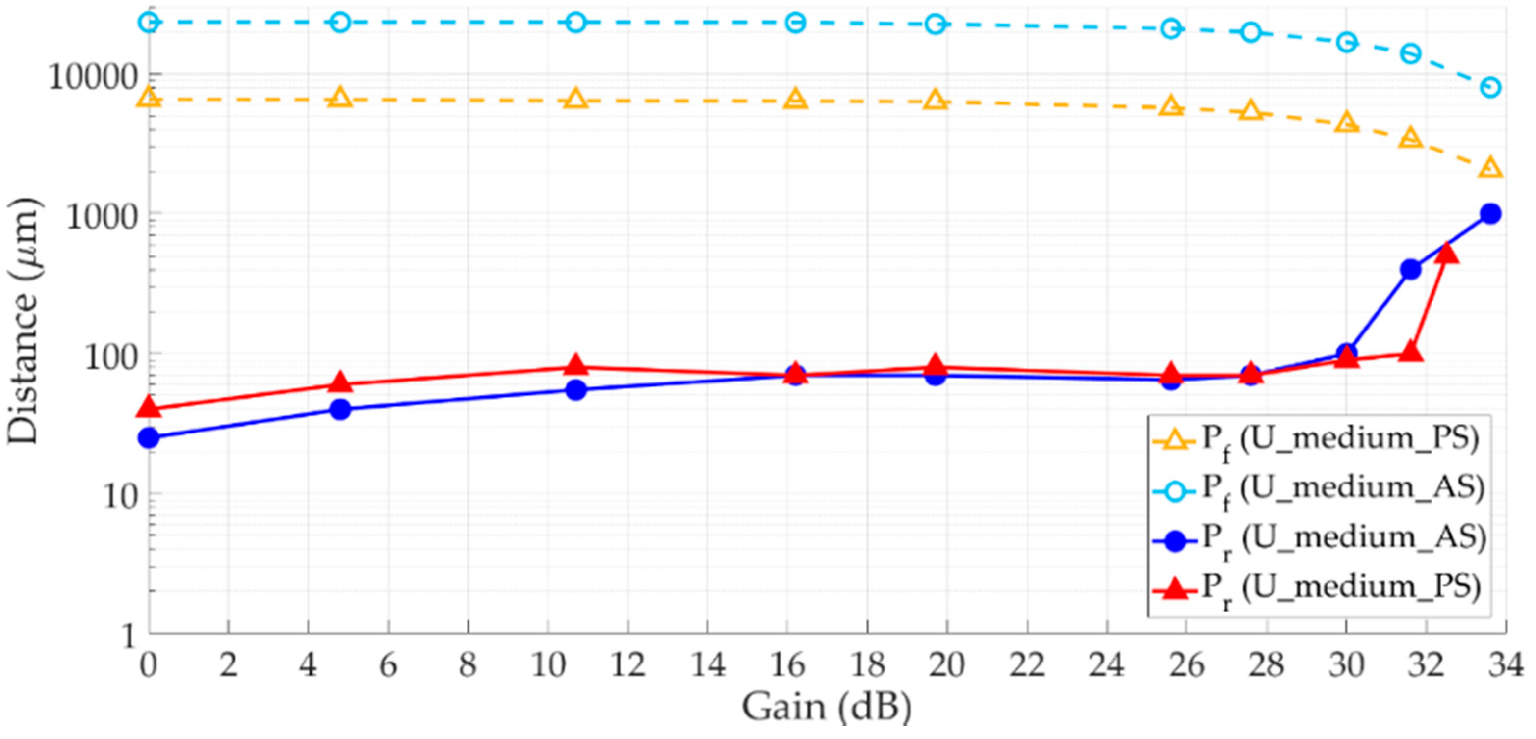
  • Free Space Zone: before Pr TX and RX are quite close each other and propagation is dominated by the direct path, since the reflected rays are much longer (in relative terms) and undergo almost normal incidence at the interfaces, which corresponds to the greatest reflection loss. Although this zone is quite limited to the near field region in the isotropic case, where RT accuracy is likely to be poor, it nevertheless extends into the far-field region for increasing antenna directivity (as explained in the following Figure 6);
  • Premium Zone: a noticeable power gain occurs between Pr and Pf compared to the free space case, likely due to a sort of guiding effect, which sets up within the silica layer. Multipath composition is constructive on average, and first triggers oscillations of the PG, finding then a regular slope with no fades in most of the cases represented in Figure 6. The spatial average of the PG decay in this zone as 1/dα, α < 2.
  • Fall Zone: beyond Pf the coherent composition of the reflected paths turns out to have intensity similar to the direct contribution, but opposite phase. Therefore, the overall received power collapses down at a rate worse than free space, as it happens in the well-known 2-rays model often referred to in mobile wireless communication when the ground presence is taken into account [22].
As clearly shown in Figure 6, this general analysis does not fully explain the U_medium_AM_0 case, where the super- and the substrate are made of air and metal, respectively. Since nup < n0, the reflected rays are totally reflected at the SiO2-Air interface as soon as the incidence angles exceeds the “critical angle” [22], as well as total reflection occurs at the SiO2-Metal interface regardless of the incidence condition. The propagating power is therefore constrained inside the SiO2 slab, the guiding effect never stops once it sets up and the premium zone infinitely extends beyond Pr.
The actual breakpoint distances are affected by several factors, like the gain (G) of the antennas, the position of the TX/RX within the SiO2 layer and its thickness. The dependence on the gain values is sketched in Figure 7. In particular, Pf is basically unaffected up to G = 25 dB, then it starts decreasing with a slope increasingly steep. Conversely, Pr rises up for increasing gain values, quite slowly up to about 20 dB, and then much more quickly beyond 30 dB. Therefore, the premium zone shrinks as the antennas become more directive, to the extent that it completely vanishes as soon as G exceeds the value corresponding to Pr = Pf. In this case, the Free Space zone directly flows into the Fall zone, and propagation conditions are never better than those experienced in free space.
This behavior may be explained by the impact of the antennas radiation pattern on the intensity of the multipath contributions. As a matter of fact, increasing the directivity boosts the amplitude of the direct path, to the detriment of the reflected ones. Therefore, the widening of the free-space zone (corresponding to the larger Pr value) for increasing gain is not surprising, since it exactly represents the distance range where propagation is primarily ruled by the direct ray. Furthermore, the larger the directivity, the poorer the power gain attained over the free space reference case, because weakening the intensity of the reflected rays impairs the multipath constructive interference the guiding effect relies on. This leads to the progressive reduction of Pf at large G values. In summary, the more directive the antennas, the stronger the signal intensity conveyed at the RX by the direct ray, thus dumping multipath fading, but the lower the further received power adding up in the premium zone because of the guiding effect. Therefore, the optimal gain value should trade off the two aspects against each other.
Figure 8 shows the sensitivity of the breakpoints to both the antennas placement within the silica layer and its thickness. It is clear that the thickness represents a crucial element, since Pf increases from about 1mm to nearly 20mm moving from the thin to the thick case. A similar trend holds for Pr, although to a lesser extent. In contrast, opposite effects are triggered by shifting the antennas within the slab, with Pr clearly increasing and instead Pf slightly decreasing as the TX/RX approach the upward/downward boundaries. Therefore, the thicker the silica layer, the wider the premium zone, whereas the closer the antennas to the interfaces, the shorter it becomes.
Although the results in Figure 8 refer to the unpacked case with passivation material and silicon respectively filling the super- and the substrate, the highlighted trends still hold in the other cases.
The package impact on the wireless channel characteristics is investigated in Figure 9, where the PG is plotted against the link distance with (continuous lines) and without (dotted lines) package. It can be first noted that the general trends previously highlighted in the unpacked case still hold when the package is also taken into account, since the two breakpoints and the corresponding three zones can be again identified after all. Moreover, larger Pf values are still detected when the superstrate is made of air, likely because the total reflection effect occurs at the SiO2-Air interface regardless of the upper layers.
The introduction of the package is fundamentally transparent as far as propagation issues are concerned if the unpacked die behaves as a full guiding structure (U_medium_AM_0 basically coincident with P_medium_AMM_0 in Figure 9a). In the other cases, a plastic package seems to affect the total PG to a lesser extent than it does when (partly) made of metal, because the presence of metal underneath the silicon bulk can enable total reflection mechanisms which are not triggered otherwise. Similarly, the presence of a plastic layer on the top of the layered stack more significantly affects the RT outcomes when the layer underneath is filled with the passivation material, since it restores the conditions for total reflection at the plastic-passivation interface, which are not fulfilled at the SiO2-passivation boundary.
In summary, the package seems more important every time its presence enforces total reflection phenomena not occurring at the inner interfaces.
The maximum communication range (dmax) is evaluated in Figure 10 for different antenna gain and packed layouts. In this study, dmax simply corresponds to the link distance where the received power equals the RX sensitivity (here set to −25 dBm, Table 1) after the signal fluctuations due to multipath fading have been spatially averaged. Compared to the reference free space case, where dmax linearly increases with G, the layered structures behave rather differently. If the gain is too low, a large amount of power is lost because of the large refraction losses undergone by the rays far from total reflection conditions in most cases. Increasing the antenna gain is therefore beneficial and the curve rises up to a peak, clearly visible in Figure 10a. Thereafter the trend is reversed and dmax starts decreasing as G keeps on increasing. As already discussed, the guiding effect taking place in the premium zone is impaired by excessive directivity levels. As the premium zone shrinks back, the communication range steadily drops towards the free space situation, that is attained as soon as the premium zone disappears (Pr = Pf). Then, propagation conditions are always worse than free-space as far as the dmax value is concerned. Therefore, very large gain values are not only useless, but even harmful, and the optimal directivity corresponds to the peak of the link distance curve. Although the peak position is affected by the silica layer thickness (Figure 10a) and by the different material combinations (Figure 10b), the outlined general analysis holds for the whole set of considered cases.
As long as the guiding mechanism can be relied on, dmax = 1 mm can be achieved with G equal to about 20 dB, that is approximately 10 dB less than the free space requirement.

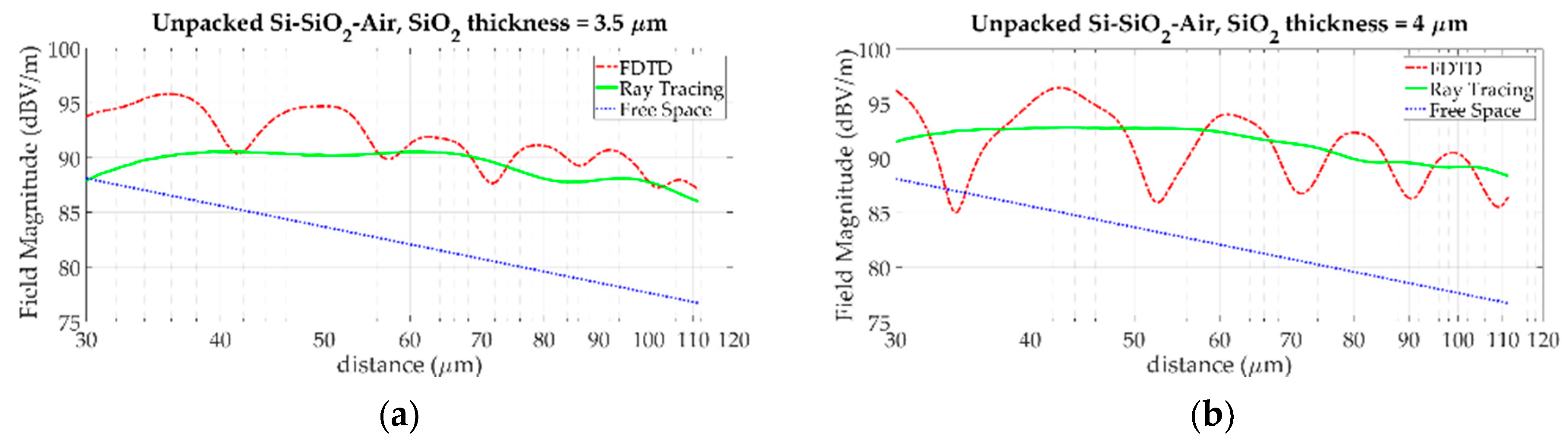
5.3. Preliminary Validation of Results

As geometrical optics is an asymptotic theory, reliable predictions should be expected when RT is run at optical frequencies. Nevertheless, several factors might impair the RT actual accuracy, e.g., related to surface propagation phenomena and/or near-field coupling effects, which has not been taken into account by the ray approach. Further numerical approximations may come from unavoidable interpolation of the antenna radiation diagram, as the rays direction of departure/arrival do not exactly coincide with the samples stored in the corresponding input file.
Because of the many difficulties in carrying out on-chip wireless measurements in the optical bands, experimental data to compare with the RT simulations are currently not available. Therefore, RT predictions have been checked against a full-wave, FDTD simulator in the unpacked case and for some different thickness of the layers. Since the full-wave simulation requires a specific antenna layout, results in Figure 11 compare the field distribution generated along the axis of the SiO2 layer by the optical antenna described in Reference [8]. The distance range is limited to about 100 μm to keep the computational burden affecting FDTD simulation under control.
The overall mean error and error standard deviation amount to −0.7 dB and 2.2 dB, respectively. Overall, the agreement is quite satisfactory, given that RT accuracy for path-loss modeling in outdoor, cellular systems usually correspond to a prediction error standard deviation of several dBs even in the best cases.
Anyway, further and deeper investigations are needed to fully assess the reliability of the proposed RT approach for on-chip propagation modeling.

6. Conclusions

Optical wireless networks on-chip can provide effective interconnection of cores in chip multiprocessor in terms of latency, layout complexity, and antenna integration. Nevertheless, inter-core communications might be thwarted by propagation losses (particularly heavy in the optical range) and/or by possible multipath effects. Characterizing the wireless channel is therefore important to predict the actual reliability of the communications and/or to design technical solutions to increase the system robustness to propagation impairments. Investigations on the main properties of on-chip wireless optical propagation have been carried out in this work through a ray tracing approach applied to a layered representation of the chip structure, with the transmitter and the receiver included in the same silica layer.
Results have highlighted the presence of three major spatial regions, namely free-space, premium, and fall zone, with different path-loss characteristics. At short distance, multipath is primarily ruled by the direct path, and the spatial average of the received power decays with distance as in free space. Then, the reflected rays become stronger and interfere constructively, thus triggering some kind of guiding effect, which results in a power gain with respect to free space. Finally, multipath interference turns round, and the received power decreases with distance at a rate steeper than free space. The size of the premium zone depends on several factors, like the antenna directivity, and position, the thickness of the layers and the materials they are made of. As a general trend, it extends for thicker silica layer, whereas it shrinks as the antennas approach the layer boundaries or become more directive. As a consequence, the communication range peaks at the antenna gain value corresponding to the optimal trade-off between the power directly conveyed at the receiver by the direct path and the additional extra-power carried by the guided reflected paths.
The presence of a package around the die affects the propagation characteristics to a limited extent, and it seems more important every time its presence enforces total reflection phenomena not occurring otherwise.
Finally, it is worth highlighting that the development of reliable propagation models represents a basic, valuable asset for the effective design of the whole network on chip, e.g., it may enable the assessment of interference issues always arising in presence of multiple wireless links. In fact, propagation awareness is ultimately necessary to estimate the signal-to-interference ratios, which are always somehow related to the overall performance of the wireless communication system.

Author Contributions

Conceptualization: F.F., M.B., and G.B.; Methodology: F.F., M.B., and G.B.; Software: F.F., M.B., and M.Z.; Validation: F.F., M.B., and M.Z.; Data Curation: F.F., M.B., M.Z., G.B., and G.C.; Writing—Original Draft Preparation: F.F., M.B., and M.Z.; Writing—Review & Editing: F.F., M.B., M.Z., G.B., G.C., P.B., and V.P.; Supervision: F.F., P.B., and V.P.

Funding

This research was funded by the Italian Ministry of Education, University and Research (MIUR) in the framework of the PRIN 2015 “Wireless Networks through on-chip Optical Technology—WiNOT” Project (20155EA8BC-PE7).

Conflicts of Interest

The authors declare no conflict of interest.

References

  1. Abdal, S.; Iannazzo, M.; Nemirovsky, M.; Cabellos-Aparicio, A.; Lee, H.; Alarcon, E. On the Area and Energy Scalability of Wireless Network-on-Chip: A Model-Based Benchmarked Design Space Exploration. IEEE Trans. Netw. 2015, 23, 1501–1513. [Google Scholar] [CrossRef]
  2. Karkar, A.; Mak, T.; Tong, K.-F.; Yakovlev, A. A Survey of Emerging Interconnects for On-Chip Efficient Multicast and Broadcast in ManyCores. IEEE Circuits Syst. Mag. 2016, 16, 58–72. [Google Scholar] [CrossRef]
  3. Deb, S.; Ganguly, A.; Ppande, P.P.; Belzer, B.; Heo, D. Wireless NoC as Interconnection Backbone for Multicore Chips: Prmises and Challenges. IEEE J. Emerg. Sel. Top. Circuits Syst. 2012, 2, 228–238. [Google Scholar] [CrossRef]
  4. Werner, S.; Navaridas, J.; Lujan, M. A Survey on Optical Network-on-Chip Architectures. ACM Comput. Surv. 2017, 50, 89. [Google Scholar] [CrossRef]
  5. Haurylau, M.; Chen, G.; Chen, H.; Zhang, J.; Nelson, N.A.; Albonesi, D.H.; Friedman, E.G.; Fauchet, P.M. On-Chip Optical Interconnect Roadmap: Challenges and Critical Directions. IEEE J. Sel. Top. Quantum Electron. 2006, 12, 1699–17055. [Google Scholar] [CrossRef]
  6. Matolak, D.W.; Kodi, A.; Kaya, S.; Di Tomaso, D.; Laha, S.; Rayess, W. Wireless Networks-on-Chips: Architecture, Wireless Channel, and Devices. IEEE Wirel. Commun. 2012, 19, 58–65. [Google Scholar] [CrossRef]
  7. Matolak, D.W.; Kaya, S. Channel Modeling for Wireless Networks-on-Chips. IEEE Commun. Mag. 2013, 51, 180–186. [Google Scholar] [CrossRef]
  8. Bellanca, G.; Calò, G.; Kaplan, A.E.; Bassi, P.; Petruzzelli, V. Integrated Vivaldi plasmonic antenna for wireless on-chip optical communications. Opt. Express 2017, 25, 16214–16227. [Google Scholar] [CrossRef] [PubMed]
  9. Zhang, Y.P.; Chen, Z.M.; Sui, M. Propagation Mechanisms of Radio Waves over Intra-Chip Channels With Integrated Antennas: Frequency-Domain Measurements and Time Domain Analysis. IEEE Trans. Antennas Propag. 2007, 55, 2900–2906. [Google Scholar] [CrossRef]
  10. Yan, L.; Hanson, G.W. Wave Propagation Mechanisms for Intra-Chip Communications. IEEE Trans. Antennas Propag. 2009, 57, 2715–2724. [Google Scholar] [CrossRef]
  11. Nafari, M.; Feng, L.; Jornet, J.M. On-chip Wireless Optical Channel Modeling for Massive Multi-core Computing Architectures. In Proceedings of the 2017 IEEE Wireless Communications and Networking Conference (WCNC), San Francisco, CA, USA, 19–22 March 2017. [Google Scholar]
  12. Yang, Y.; Li, Q.; Qiu, M. Broadband nanophotonic wireless links and networks using on-chip integrated plasmonic antennas. Sci. Rep. 2016, 6, 19490. [Google Scholar] [CrossRef] [PubMed] [Green Version]
  13. Garcia-Meca, C.; Lechago, S.; Brimont, A.; Griol, A.; Mas, S.; Sanchez, L.; Bellieres, L.; Losilla, N.S.; Martì, J. On-chip wireless silicon photonics: From reconfigurable interconnects to lab-on-chip devices. Light Sci. Appl. 2017, 6, e17053. [Google Scholar] [CrossRef] [PubMed]
  14. Wu, Z. Electromagnetic Surface Waves. In Encyclopedia of RF and Microwave Engineering; Wiley and Sons: Hoboken, NJ, USA, 2005; pp. 1270–1280. [Google Scholar]
  15. Barlow, H.M.; Cullen, A.L. Surface Waves. Proc. IEEE Part III 1953, 100, 329–341. [Google Scholar] [CrossRef]
  16. Collin, R.E. Surface Waveguides. In Field Theory of Guided Waves, 2nd ed.; Wiley-IEEE Press: New York, NY, USA, 1990; pp. 697–748. ISBN 978-0879422370. [Google Scholar]
  17. Rich, J.C. The launching of a plane surface wave. Proc. IEE Part B Radio Electron. Eng. 1955, 102, 237–246. [Google Scholar] [CrossRef]
  18. Rabaey, J.M.; Chandrakasan, A.; Nikolic, B. Digital Integrated Circuits: A Design Perspective, 2nd ed.; Pearson: London, UK, 2002; pp. 41–69. ISBN 978-0130909961. [Google Scholar]
  19. Deng, T.; Zhang, Y.P. On-Chip Antennas. In Handbook of Antenna Technologies; Springer: Singapore, 2016; pp. 1565–1584. ISBN 978-981-4560-43-6. [Google Scholar]
  20. Pan, S.; Capolino, F. Design of a CMOS On-Chip Slot Antenna with Extremely Flat Cavity at 140 GHz. IEEE Antennas Wirel. Ppropag. Lett. 2011, 10, 827–830. [Google Scholar] [CrossRef]
  21. Narde, R.S.; Mansoor, N.; Ganguly, A.; Venkataraman, J. On-Chip Antennas for Inter-Chip Wireless Interconnections: Challenges and Opportunities. In Proceedings of the 12th IEEE European Conference on Antennas and Propagation (EuCAP2018), London, UK, 9–13 April 2018. [Google Scholar]
  22. Bertoni, H.L. Wireless Propagation for Modern Wireless Systems; Prentice Hall: Upper Saddle River, NJ, USA, 2000; pp. 86–106. ISBN 978-0130263735. [Google Scholar]
  23. Burnside, W.; Burgener, K. High frequency scattering by a thin lossless dielectric slab. IEEE Trans. Antennas Propag. 1983, 31, 104–110. [Google Scholar] [CrossRef] [Green Version]
Figure 1. Sketch of the spatial and surface wave concepts.
Jlpea 08 00039 g001
Figure 2. On-chip radio channel as a layered medium.
Jlpea 08 00039 g002
Figure 3. Layered structures for the unpacked (a) and the packed (b) cases.
Jlpea 08 00039 g003
Figure 4. RT propagation in layered representation of an integrated circuit: examples of optical rays in the unpacked (a) and in the packed (b) case.
Jlpea 08 00039 g004
Figure 5. Examples of antenna radiation patterns resulting for different gain values.
Jlpea 08 00039 g005
Figure 6. Path gain vs. TX-RX distance in the unpacked case with medium thickness of the silica layer, different substrate and superstrate, and assuming isotropic radiators.
Jlpea 08 00039 g006
Figure 7. Pr and Pf distances vs. TX/RX antenna gain. Unpacked case with medium thickness of the silica slab and silicon underneath.
Jlpea 08 00039 g007
Figure 8. Sensitivity of the rise (a) and the fall (b) points to the silica slab thickness and the antenna placement. Isotropic, unpacked case with passivation and silicon filling the super- and the substrate, respectively.
Jlpea 08 00039 g008
Figure 9. Comparison between unpacked and packed arrangements, for medium thickness of the silica layer and isotropic radiators. The superstrate is filled with air (a) or with a passivation material (b).
Jlpea 08 00039 g009
Figure 10. Link distance vs. antenna gain for the packed scenario and middle placed TX/RX. (a) Plastic package, up-layer passivation, different thickness (b) comparison between different packed layouts, medium thickness.
Jlpea 08 00039 g010
Figure 11. Comparison between RT and FDTD prediction of the field distribution along the axis of the silica layer. Thickness of the silica layer equal to 3.5 μm (a) and 4 μm (b).
Jlpea 08 00039 g011
Table 1. Major input parameters for the RT simulator.
ParameterValue
Δhthin: 6 μm; medium: 10 μm; thick: 14 μm
Δhup2 μm
Δhdown625 μm
n01.44 (SiO2)
ntop1.5 (plastic)
nup1 (Air) or 2 (passivation)
ndown3.47 (Si, perfect metal otherwise)
nbottom1.5 (plastic, perfect metal otherwise)

