3.1. Operating Principle
As shown in
Figure 2 [
8], a piezoelectric transducer can be modeled as a sinusoidal current source
iP(
t) =
IP sin(2π
fPt), in parallel with a parasitic plate capacitor,
CP and a parasitic resistor,
RP. The amplitude of a piezoelectric transducer current,
IP varies with the mechanical excitation level of the piezoelectric transducer while
fP represents the excitation frequency of the piezoelectric transducer.
A typical full-wave bridge rectifier consists of four diodes. The major problem of using an off-chip diode in a conventional rectifier circuit is that it results in a substantial voltage drop due to the diode turn-on voltage (
Vd), which is typically 0.5~0.7 V. This large turn-on voltage causes a significant loss in a conventional full-bridge rectifier. In addition, charging and discharging of the plate capacitance of a piezoelectric transducer results in a loss of available charges from the transducer. To overcome these problems, a CMOS based full-bridge rectifier with a switch-only circuit in parallel with a piezoelectric transducer is proposed in [
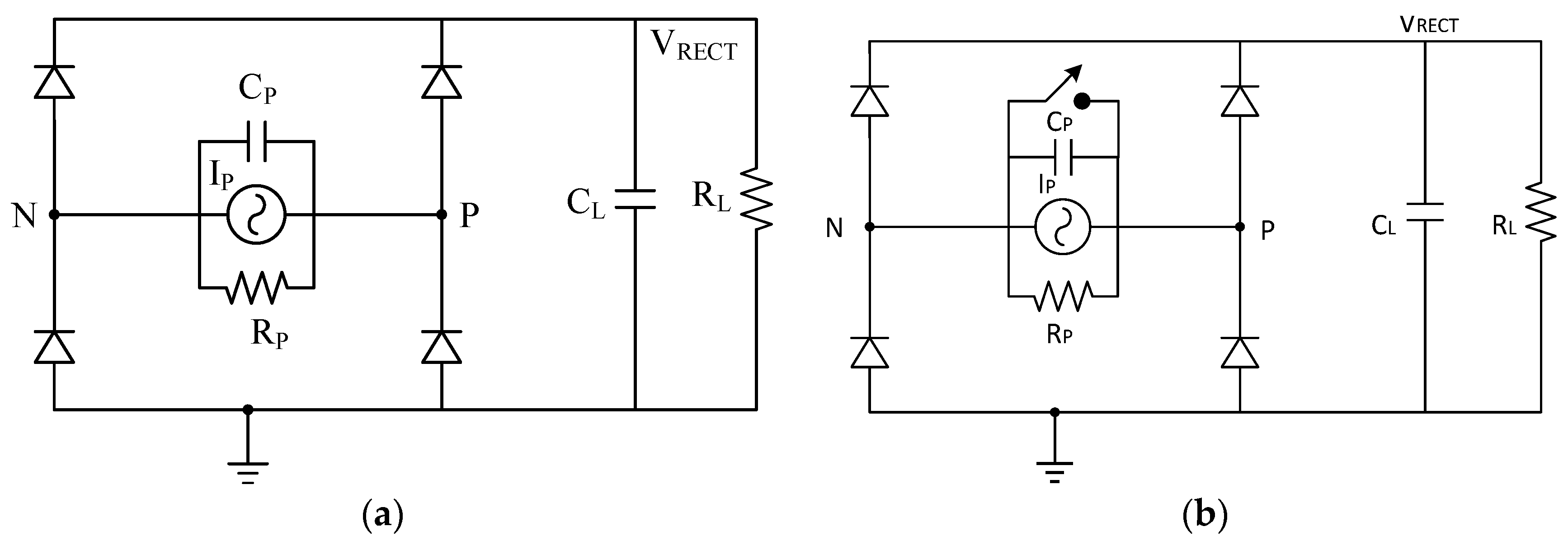
8]. In the switch-only (SO) rectifier scheme, a switch is turned on whenever the transducer current crosses a zero which helps discharge the capacitor,
CP. Unlike a conventional rectifier, this process allows the SO rectifier not to discharge from (
VRECT + 2
Vd).
Figure 3a,b show a conventional full-bridge rectifier and a rectifier with switch-only scheme, respectively. To reduce the voltage-drop across a diode which affects the conversion efficiency, a CMOS based full-wave bridge rectifier with a switch is presented in this paper. The advantages of this proposed design include the ability to power the proposed circuit to operate without requiring any off-chip components even though the power generated by the SO rectifier is less than that of the bias-flip or other power enhanced structures. This allows more flexibility to integrate the circuits with an integrated system. In addition, by using a separate control signal for the PMOS switch in a SO rectifier, the current for charging and discharging of
Csg of the PMOS device can be effectively reduced, which increases the available energy transfer time to the output load. In addition, a switch can be added in between
VN and
VP inputs of a piezoelectric transducer to reduce the wasted charges which is used to charge or to discharge the parasitic capacitance of a piezoelectric device.
Figure 4 shows the circuit diagram of the proposed circuit as well as the system reported in [
1,
3,
8].
3.2. Proposed Active Full-Wave Rectifier
Figure 4a shows the full-wave rectifier structure reported in [
1,
3,
8]. Due to the cross-coupled nature of the circuit, it requires a current and time to charge and discharge
Csg of the PMOS switch charged by a piezoelectric transducer directly prior to being turned on and off. Therefore, to turn on the PMOS switch in order to charge
Csg the input voltage from a piezoelectric transducer,
VPN should be greater than |
Vthp|. Therefore, the available transfer time of energy from a piezoelectric transducer will be reduced because of the time required to charge
Csg.
However, in the proposed active rectifier circuit as shown in
Figure 4b, the PMOS on/off are controlled by the NMOS turning on/off signal and are driven by output voltage powered buffer. Therefore, the proposed system does not pose problems associated with the design reported in [
1,
3,
8]. As shown in
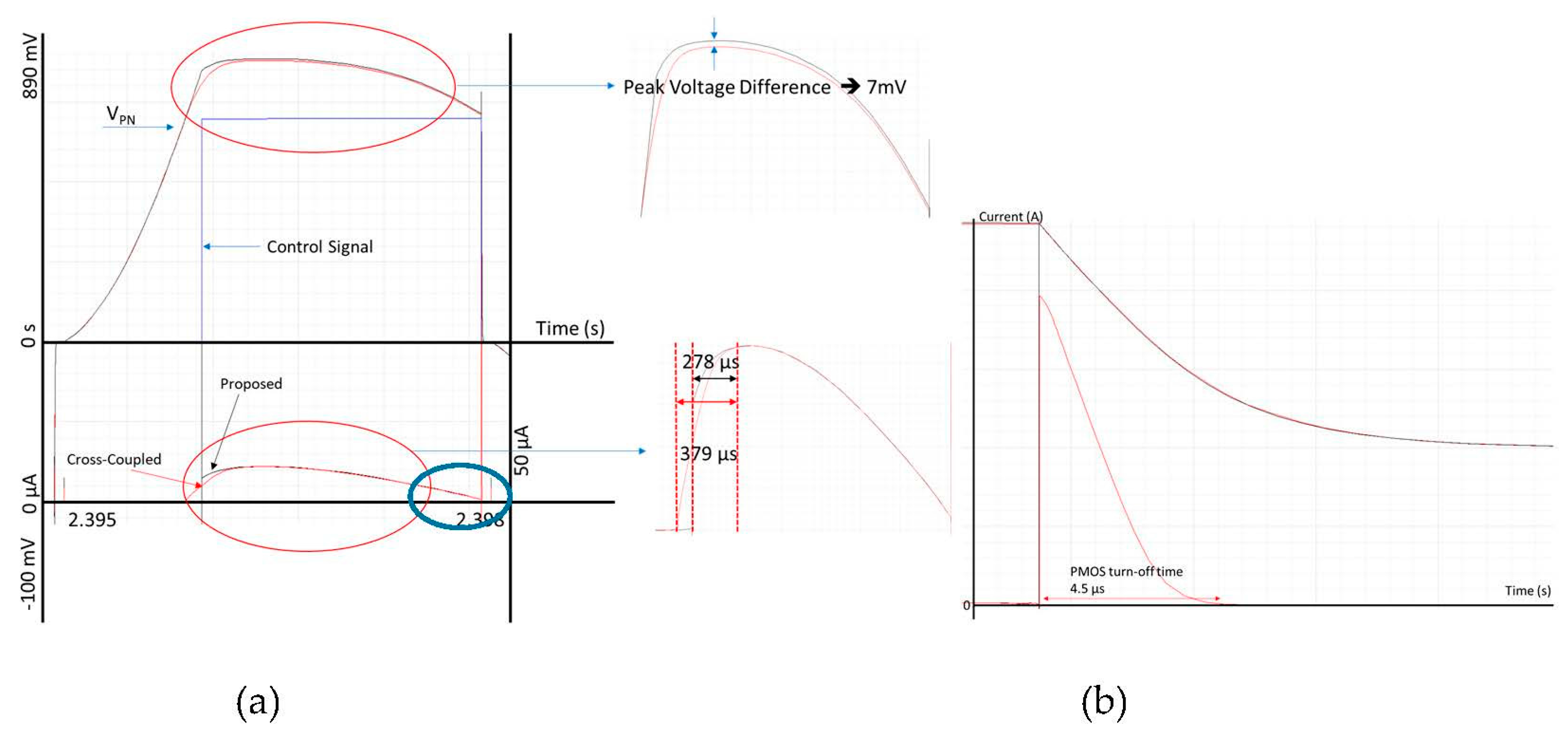
Figure 5, the time required to charge
Csg is about 100 µs (about 39% less time to reach the peak current from a piezoelectric transducer) less than cross-coupled system presented in [
1,
2,
8]. The PMOS off-time also has been reduced as shown in
Figure 5b. The proposed system instantly discharges
Csg, and as a result, the off time is in the nano-second range even though the off-time of the cross-coupled system is 4.5 µs. Therefore, more energy from a piezoelectric transducer can be transferred to the output resulting in the
VPN voltage ([
VP-
VN] of a piezoelectric input voltage) being about 0.7% higher than that of a cross-coupled based active rectifier with the same load and piezo input. Although 0.7% can be considered as a small improvement in a system, for low input power systems such as the one proposed in this paper, every available energy should be squeezed so that more available energy can be transferred to the output. In addition, if the excitation frequency as well the force applied to a piezoelectric transducer are lowered, then, charging time will be increased because of less available charges from a piezoelectric transducer. As a result, the voltage amplitude of
VPN will be lowered so as
VRECT. In addition, since the proposed energy harvesting system can handle more energy than a cross-coupled rectifier, the output voltage,
VRECT, is higher than that of the cross-coupled circuit.
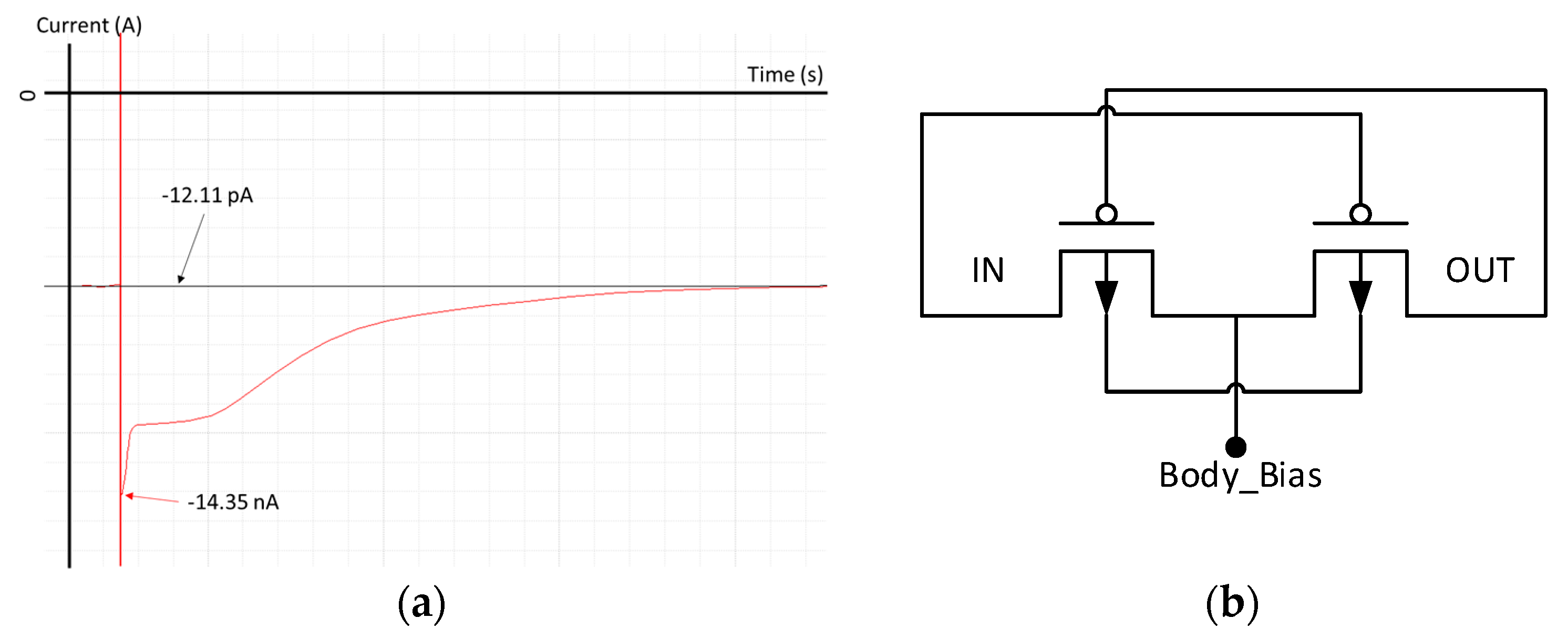
Figure 6a,b show the body leakage current and the body bias control circuit utilizing the leakage current, respectively. With the help of simple implementation of body-bias control circuit, the proposed system can achieve lower body leakage current compared with cross-coupled system reported in [
1,
3,
8].
Figure 6 shows the body leakage current of the circuit that has been used to control the body bias. In
Figure 6b,
IN is connected to the
VRECT,
OUT is connected either
VP or
VN, and the body-bias port is connected to the body of the PMOS switch. As shown in
Figure 6a, the leakage current in the proposed system is −12.11 pA (black line) while the leakage current in cross-coupled system is −14.35 nA (red line), which is a huge improvement. With the help of all the above improvements, the output voltage from a proposed active rectifier is 698 mV while that of the rectifier with cross-coupled based is 694 mV.
The proposed switch-only active rectifier as well as the cross-coupled active rectifier with switch-only are simulated with the same MOSFET sizes as well as the same input piezo current. The only difference between the two schemes is the top PMOS gate control methods.
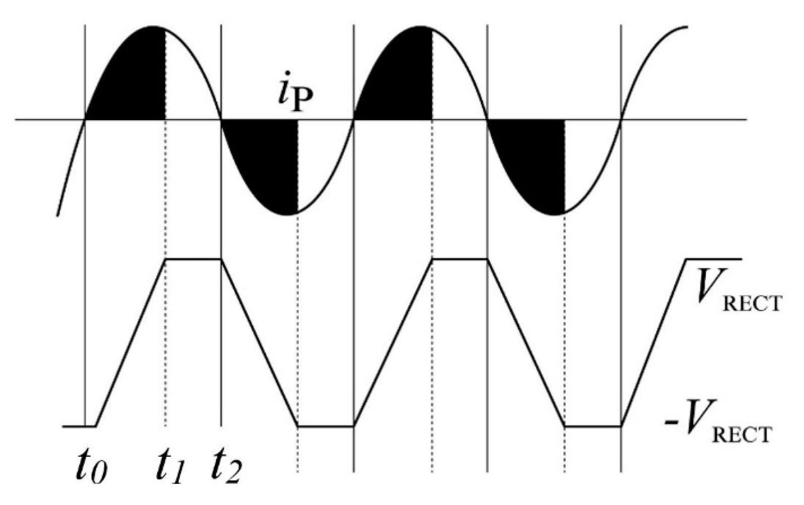
Figure 7 shows the waveform of the piezoelectric transducer current,
iP versus
VRECT of a conventional full-wave rectifier. The shaded regions show the wasted energy due to charging and discharging of a parasitic capacitor,
CP.
It is evident from the figure that a significant amount of energy is lost due to the charging and discharging actions of
CP. In
Figure 7, the difference between
t0 to
t1 represents the wasted energy when
iP is used to charge
CP. The total charge available in full-bridge rectifier can be written as,
where
Vp is the amplitude of the open circuit voltage of the piezoelectric transducer.
The piezoelectric transducer current,
iP, has to charge
CP from
VRECT to −
VRECT in every cycle before turning on a diode in a conventional full bridge diode. Therefore, charge lost in every cycle can be written as [
8],
From Equations (1) and (2), the actual charge that used to charge
CL in
Figure 3 can be written as [
8],
Multiplying Equation (3) by the output voltage of the piezoelectric transducer,
VRECT provides the total energy delivered to
CL. Therefore, the total energy can be written as [
8],
Since the piezoelectric transducer operates at a frequency,
fP the total power delivered to the output capacitor,
CL by the conventional full-bridge rectifier can be expressed as [
8],
Using Equation (5), the maximum available power is obtained when
VRECT =
VP/2, and can be expressed as
To reduce this unwanted energy loss or to increase the energy transfer from a piezoelectric transducer, one effective scheme involves inserting a switch in between the inputs of the piezoelectric transducer,
VP and
VN as shown in
Figure 4.
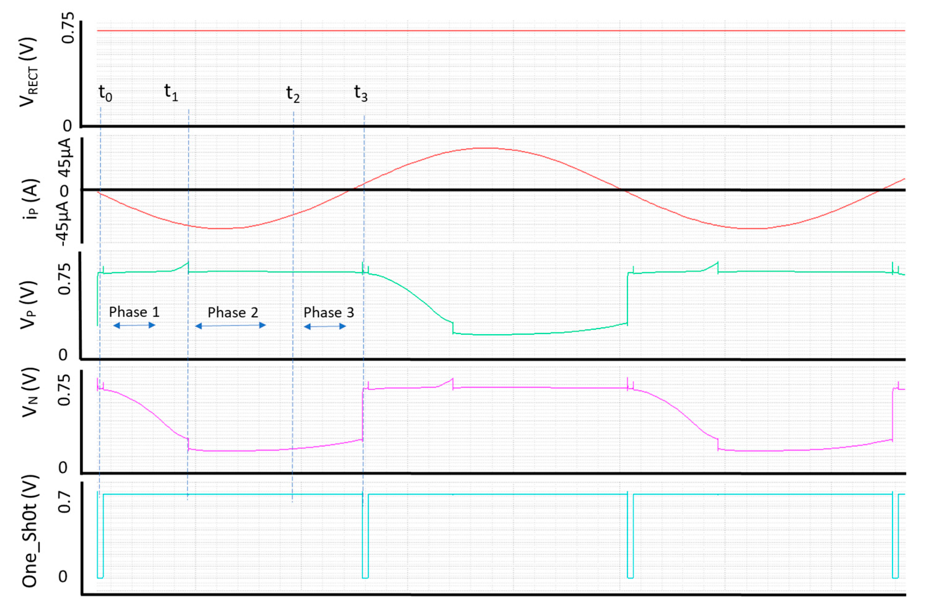
Figure 8 shows the steady-state operation of the proposed full-wave rectifier. It can be seen from
Figure 8 that the operation of the proposed full-wave rectifier can be divided into three phases. In phase 1 between
t0 to
t1, a sinusoidal current,
iP from a piezoelectric transducer starts charging a parasitic capacitor,
CP. Unlike a conventional piezoelectric transducer as shown in
Figure 3, time for charging of
CP has been reduced significantly because of the inclusion of a switch in between
VP and
VN. In
Figure 9, it can be seen that as the one-shot turns on, the
VP and
VN terminals are shorted instantly and therefore it does not have to charge from its previous value, rather it starts from zero. In a conventional rectifier, when
iP is changing its polarity from positive to negative,
CP should be discharged from (
VRECT + 2
Vd) to zero and charged from zero to −(
VRECT + 2
Vd). In phases 2 and 3, since the charging of a parasitic capacitor
CP has been completed, the energy can be transferred to the output capacitor,
CL through the full-wave rectifier.
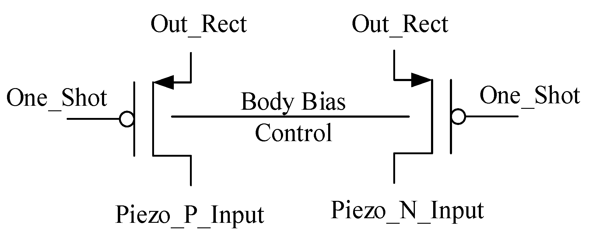
Figure 9 shows the switch inserted in between
VP and
VN of a piezoelectric transducer which allows the capacitor to discharge to zero. The working principle for the one-shot signal switch is very simple.
Whenever a piezoelectric transducer crosses the zero point, the one-shot control circuit as shown in
Figure 10 is designed to provide a short pulse which shorts the input ports of a piezoelectric transducer to reset the voltages
VP and
VN. This shorting action will help improve the efficiency of the piezoelectric energy harvesting circuit by reducing a waste charge. Therefore,
iP does not have to charge or discharge
CP from ±(
VRECT + 2
Vd) but rather from zero to (
VRECT + 2
Vd). The bottom two NMOS switches are controlled by a low-power comparator while the top two PMOS switches are controlled by
P_Control and
N_Control bar signals. All the control circuits as well as the comparator are powered by the harvested supply voltage,
VRECT.
In the proposed full wave rectifier, the charge lost in every cycle can be denoted by [
8],
The charge available can be calculated as [
8],
Therefore, the total power delivered to the output load
CL can be expressed as follow [
8].
Comparison of Equations (3) and (8) reveals that the charge lost is reduced by about 50%. Therefore, inserting a switch in between
VP and
VN of a piezoelectric transducer can save a substantial amount of energy. All the control circuits in this proposed active rectifier are powered by the output voltage,
VRECT derived from the harvested energy.
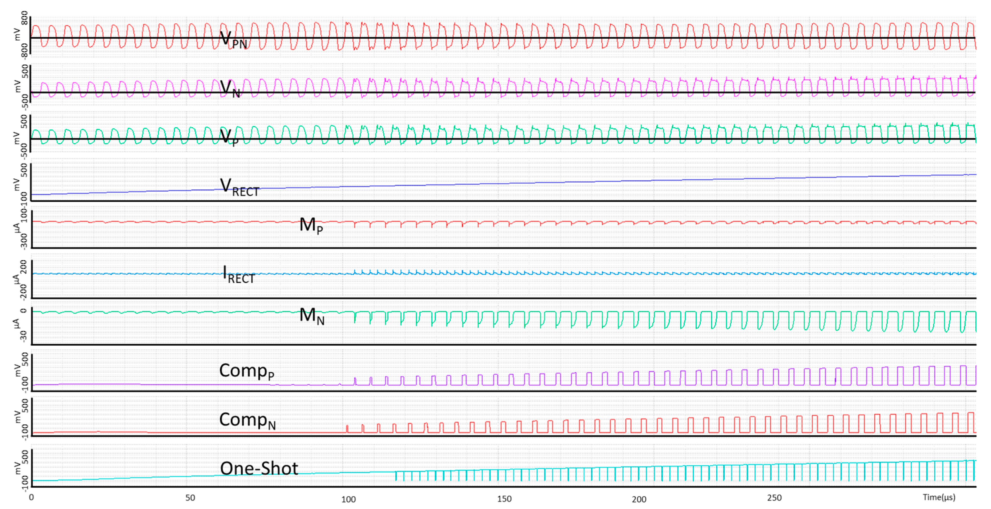
Figure 11 illustrates the start-up operation of the circuit. For the start-up of the rectifier operation, all the control circuits including the comparators are not working until
CL is charged properly since no charge is accumulated in
CL initially. As shown in
Figure 11, leakage current flows through both PMOS(
MP) and NMOS(
MN) as the input of a piezoelectric transducer starts increasing thereby slowly charging
CL. The initial charging current derived from this leakage current is in nano-ampere range. The time required to charge
CL is approximately 120 µs and the resulting harvested supply power all the control circuits including the comparators. Proper working of all control signal starts at around 180 µs.
CompP and
CompN are the output waveform of comparators, and
One-Shot is the output waveform of the One-Shot control signal.
CompP and
CompN are represent
P_Control and
N_Control signals in
Figure 4b.


