A Multi-Channel Low-Power System-on-Chip for in Vivo Recording and Wireless Transmission of Neural Spikes

Abstract
:1. Introduction
- • preserve the information needed for single neuron identification;
- • reduce the throughput and thus the power consumption, since the power needed to the antenna is directly proportional to the bit rate [8];
- • keep the bandwidth limited to few MHz, thus reducing the probability of RF interference and verifying the possibility to make in the future the system compliant to Medical Implanted and Communication Service (MICS) or Industrial Scientific and Medical (ISM) bands, in the 402–405 MHz and 902–928 MHz frequency range, respectively.
2. System Architecture
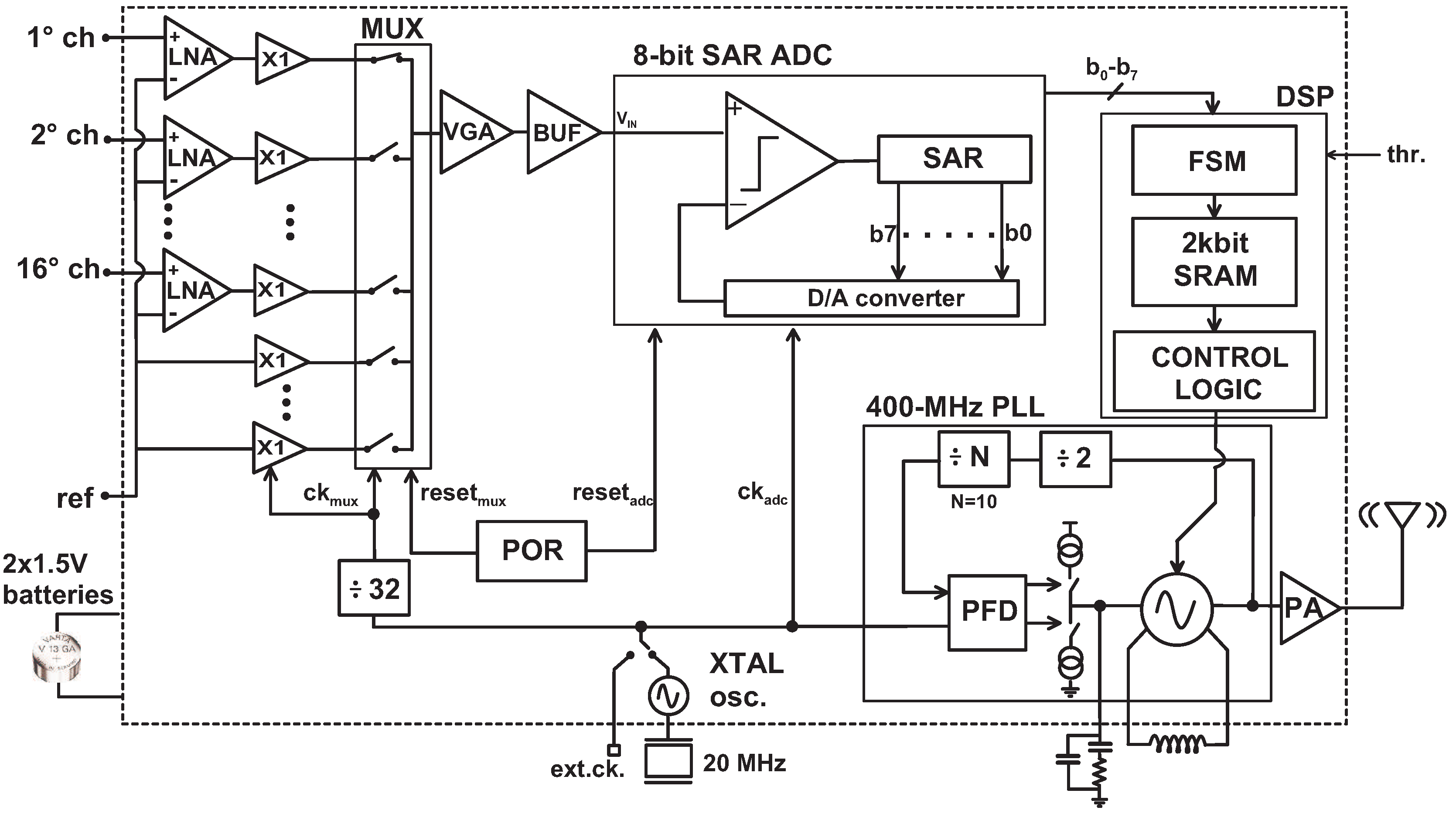
2.1. Wireless Recording Unit
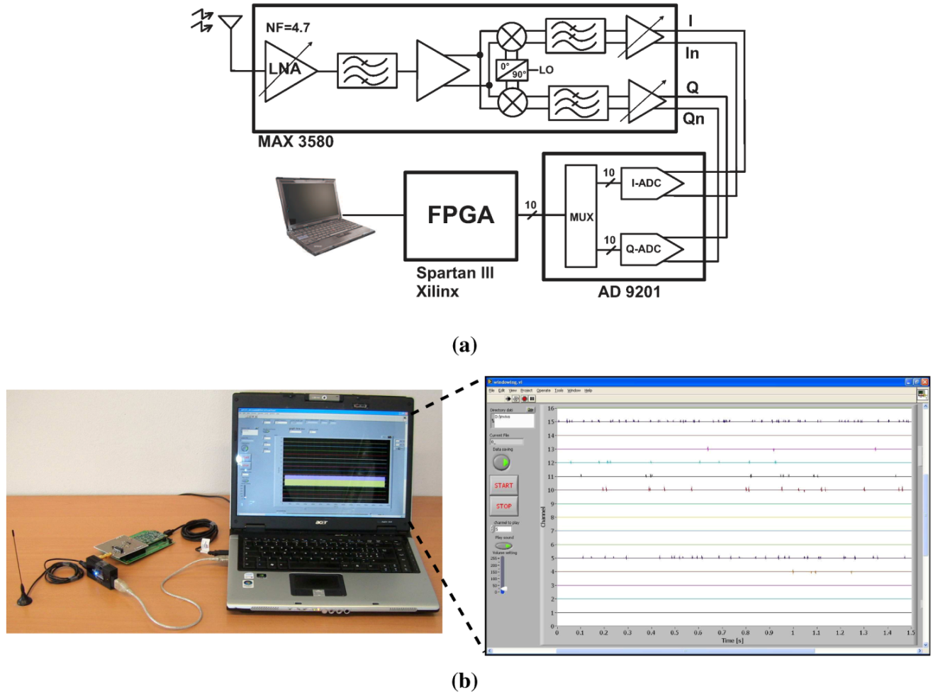
2.2. Receiver and Graphical User Interface
3. Circuit Design
3.1. Analog Front-End
 , set to –67 by taking
  pF and C2 = 150 fF. The high-pass pole frequency is placed below 10 Hz to reject the offset and the slow voltage drift of the electrode. A tunable GM -C high-pass filter with a cut-off frequency fHP of about 300 Hz is introduced after the first stage. It is designed to reject the low-frequency signals, such as Local Field Potentials (LFPs) in the
  Hz frequency range that can prevent a correct detection of the neural spikes or even saturate the amplifier, and cuts off the input-referred
  noise due to the pseudo-resistors of the first amplification stage. After the selective high-pass filter, a second non-inverting gain stage is added to provide further signal amplification and to define the high frequency cut-off, fLP. The stage is a single-ended capacitive-coupled voltage amplifier with a gain
  , achieved by using
  pF and
  fF. A capacitive-coupled structure was preferred to a purely resistive feedback amplifier to minimize the current drawn by the OTA output stage. The DC voltage at the amplifier input is determined by the pseudo-resistor elements in the feedback path, while the low-pass cut-off frequency is set by the gain-bandwidth product of the operational amplifier (GBWP2 ) to about
  kHz. Note that at very low frequencies this non-inverting stage has a unity gain in order not to amplify the offset of the operational amplifier.
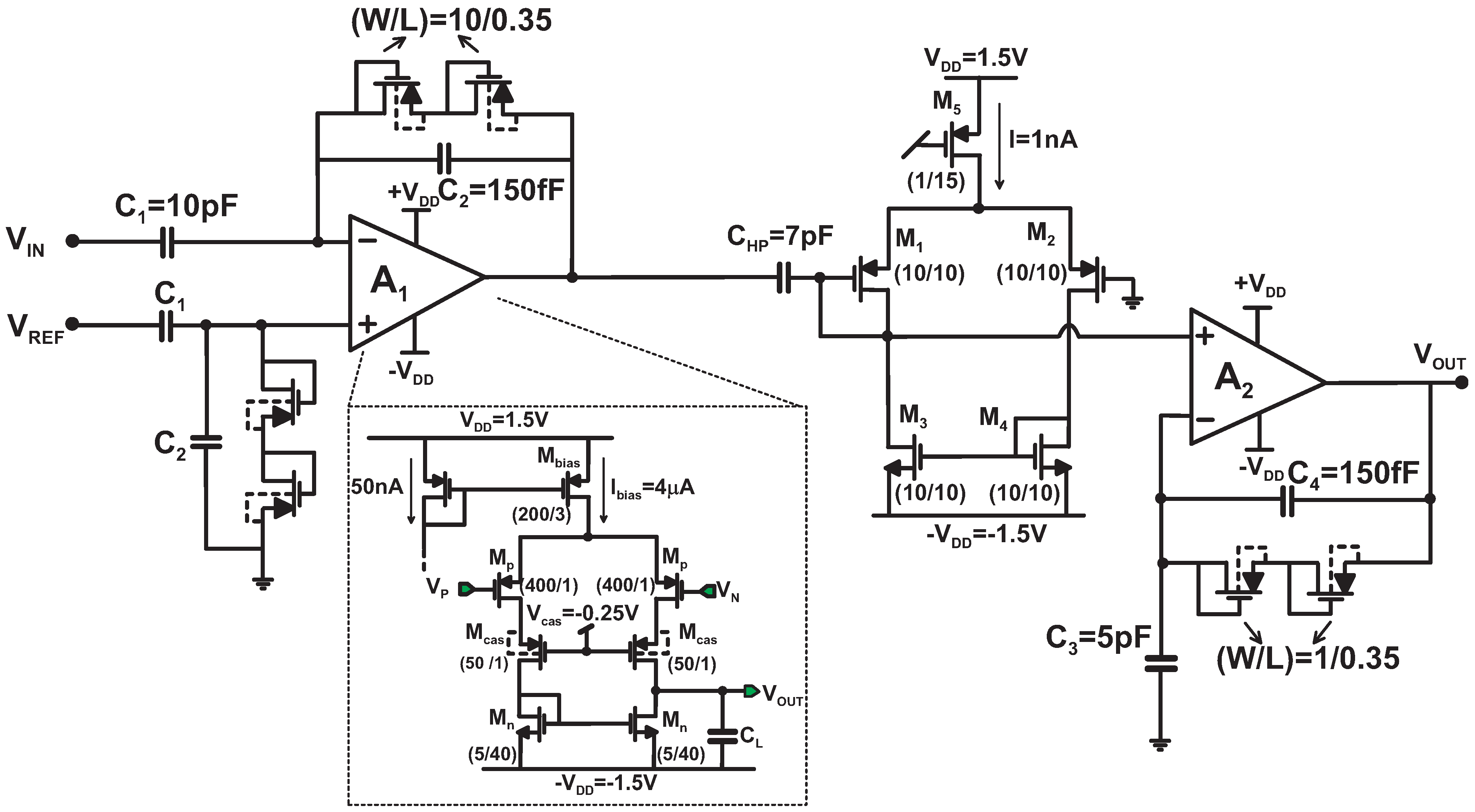
3.1.1. Noise Analysis and First Stage Sizing

 is the input-referred voltage noise of the first-stage OTA. Equation (1) highlights that Cp, which is mainly determined by the input transistor dimensions, cannot be increased too much without compromising the overall input-referred noise. On the other hand, it is well known that large-area input transistors are required to minimize the OTA flicker noise. Therefore, to achieve the best overall performance these two contradictory requirements have to be balanced. Furthermore, according to Equation (1), the first stage gain, G1, can be increased maximizing C1. Its value is limited by the electrode impedance, whose capacitive component is in the 160–320 pF range. The choice of C1 = 10 pF, C2 = 150 fF, thus
  , results in an upper limit of 0.5 pF for the parasitic capacitance Cp. which guarantees sufficient margin to keep under control the 1/f noise at a cost of a marginal 10% increase in the overall amplifier noise with respect to the ideal OTA [see Equation (1)]. In such a design,
  and are almost the same; therefore, both terms will be denoted with the same symbol, .
| Transistor |  [mV] [mV] | IC | gm [μA/V] | ro [M  ] ] |
|---|---|---|---|---|
| Mp | 110 | 0.075 | 52.3 | 5.1 |
| Mn | 490 | 51 | 7.76 | 108 |
| Mcas | 24 | 0.36 | 43.7 | 8.2 |

 must be fulfilled, i.e.,
  . Under this assumption the total noise power density results:
 equal to 2/3 for transistors working in strong inversion or
  in weak-inversion (
  ) [12]. In order to minimize the thermal noise without increasing the current consumption, the Mp transistors have to work in the weak inversion region, where the transconductance is maximum. Its value can be estimated from the EKV model [13], valid in all regions of inversion:


 kHz
kHz  kHz. For an upper limit of 3 μVrms for the thermal noise contribution in this noise band, a minimal Ibias value of about 3 μA is required; to be conservative, we set Ibias = 4 μA .
 ). Considering that for the adopted technology
  V2F and
  5 fF/μm2 and setting a noise corner frequency lower than 100 Hz, the input PMOS transistors were sized with
  m2. This sizing results into a stray OTA input capacitance Cp of approximately 500 fF, which does not excessively impair the equivalent input noise. Moreover, in order to fulfill the requirement , the settings
  m and
m and  m were applied, thus forcing these devices to work in the strong inversion region (see Table 1). For this choice of the transistor lengths, cascoding of the input differential pair is needed to not to degrade the output resistance and, thus, to not to lower the amplifier gain. The introduction of Mcas guarantees an output resistance
  and an amplifier gain
  dB.
dB.
 is the input-referred rms noise, Itot is the total supply current and BW is the bandwidth of the amplifier. In this limit, the minimum NEF achievable with a simple differential stage can be estimated from Equations (6) and (7) leading to a value of
  [15]. However, in our design the contribution to the thermal noise of the current mirror transistors cannot be completely neglected. In fact, even if Mp transistors work in weak-inversion and Mn FETs are biased in strong inversion region, the transconductance ratio is only about 7 (see Table 1). Considering the general expression of the transconductance given by Equation (4) and the total input-referred thermal noise given by the first two terms of Equation (2), the theoretical NEF for this preamplifier becomes:
 , and ICn is the inversion coefficient of current mirror transistors. In reality, the NEF of the proposed amplifier is slightly larger compared to this theoretical limit for three main reasons:
- • The transconductance of the input transistors is slightly lower than
![Jlpea 02 00211 i108]() since their inversion coefficient is larger than zero. For the present design, the input transistor IC is 1.075 (see Table 1), and consequently the rms input noise and the NEF increase by a factor of 1.034.
since their inversion coefficient is larger than zero. For the present design, the input transistor IC is 1.075 (see Table 1), and consequently the rms input noise and the NEF increase by a factor of 1.034. - • The input-referred noise of the overall amplifier is larger by a factor
![Jlpea 02 00211 i111]() than the one of the first operational amplifier, as stated by Equation (1). Taking into account that the parasitic input capacitance is approximately 0.5 pF, mainly due to the OTA input transistors, this factor is equal to 1.065. A further contribution derives from the strays associated with the input capacitor plates that was drastically reduced by connecting the capacitor bottom plate (which has the largest parasitism) to the amplifier input and by connecting the top plate to the OTA terminal. In this way, a parasitic capacitance larger than 1.5 pF was avoided.
than the one of the first operational amplifier, as stated by Equation (1). Taking into account that the parasitic input capacitance is approximately 0.5 pF, mainly due to the OTA input transistors, this factor is equal to 1.065. A further contribution derives from the strays associated with the input capacitor plates that was drastically reduced by connecting the capacitor bottom plate (which has the largest parasitism) to the amplifier input and by connecting the top plate to the OTA terminal. In this way, a parasitic capacitance larger than 1.5 pF was avoided. - • The current drawn by the second amplifying stage contributes to the total current in Equation (7) but does not lower the input-referred thermal noise. Therefore, the NEF increases by a factor of
![Jlpea 02 00211 i114]() , where I1 and I2 are the currents drawn by the first and the second operational amplifier respectively.
, where I1 and I2 are the currents drawn by the first and the second operational amplifier respectively.


 mV
mV  while the negative swing is about 1 V
  , thus assuring a maximum amplitude for the input signal of about 7 mV.
3.1.2. Second Amplifying Stage
 (i.e., 1/10 of the dominant contribution), a minimum current of 100 nA is needed in the input differential pair of the second op-amp. To be conservative, we set the bias current to 200 nA in the first stage, while a current of 100 nA is drawn by the second stage.
3.1.3. High-Pass Filter Design and Optimization
 law and is given by:

 fHP, where fHP is the cut-off frequency of the GM -C high-pass filter. For frequency above f1, the input-referred power spectral density due to both the pseudo-resistors of the first stage and to the GM -C filter can be written as:
 is the output current noise of the high-pass filter. For simplicity, let us assume that the current noise generated by the GM cell (
  ) can be written as
  . Equation (12) becomes:

 ratio while a large capacitor value CHP is needed to reduce the second term. In practice, the GM cell is a simple differential stage (see Figure 3) whose bias current can be externally tuned. Because a small bias current (I
  1 nA) is needed to synthesize a high value resistance, all the transistors work in weak-inversion region and their transconductance is
  . The current noise of this configuration is therefore:
 larger than that of a resistor RHP and this factor has to be added in the second term of Equation (14).
 Hz (with
  Hz) and
  pF.
pF.3.1.4. Line Buffer and Multiplexer
3.2. Analog to Digital Converter
- • The maximum amplitude for an extra cellular action potential is ~ 1 mV [17] while the minimum signal is about 10 μV, the latter being determined by the typical input noise due to neural background activity and electrode impedance [18]. Therefore, the ratio between the Full Scale Range (FSR) and the ADC least significant bit, i.e., the dynamic range of the converter, should be better than 1 mV/10 μV
![Jlpea 02 00211 i154]() 100 . This results in a converter resolution larger than 6.35 bit.
100 . This results in a converter resolution larger than 6.35 bit. - • The ADC quantization noise has to be kept much lower than the minimum detectable signal, i.e., the rms input noise. This requirements translates into:
![Jlpea 02 00211 i156]() where G is the amplifier gain and n is the number of converter bits. The worst-case condition occurs for the minimum gain of the amplification chain, which is set by the ratio between the FSR and the maximum amplitude of the input signal, Amax :
where G is the amplifier gain and n is the number of converter bits. The worst-case condition occurs for the minimum gain of the amplification chain, which is set by the ratio between the FSR and the maximum amplitude of the input signal, Amax :![Jlpea 02 00211 i160]() In the present design we set Gmin
In the present design we set Gmin![Jlpea 02 00211 i141]() 2000 and thus:
2000 and thus:![Jlpea 02 00211 i163]()


- • The noise in the sampling phase has to be significantly smaller than the quantization noise. Thus, the total capacitance of the array, CTOT, must satisfy the condition:
![Jlpea 02 00211 i166]() which clearly is not a limit factor, resulting in CTOT much larger than about 1 fF.
which clearly is not a limit factor, resulting in CTOT much larger than about 1 fF. - • The LSB capacitance has to be sufficiently accurate and it has to fulfill the following requirement [19]:
![Jlpea 02 00211 i167]() where
where![Jlpea 02 00211 i168]() m and Ac are the Pelgrom mismatch parameter and the least significant bit (LSB ) capacitor area, respectively.
m and Ac are the Pelgrom mismatch parameter and the least significant bit (LSB ) capacitor area, respectively. ![Jlpea 02 00211 i169]() From Equation (20) Ac has to be larger than (4.5 μm)2, which implies
From Equation (20) Ac has to be larger than (4.5 μm)2, which implies ![Jlpea 02 00211 i173]() fF, considering a specific capacitance of 1 fF/μm2.
fF, considering a specific capacitance of 1 fF/μm2.


 fF was employed as unit capacitor, resulting in a total capacitance of
  pF.
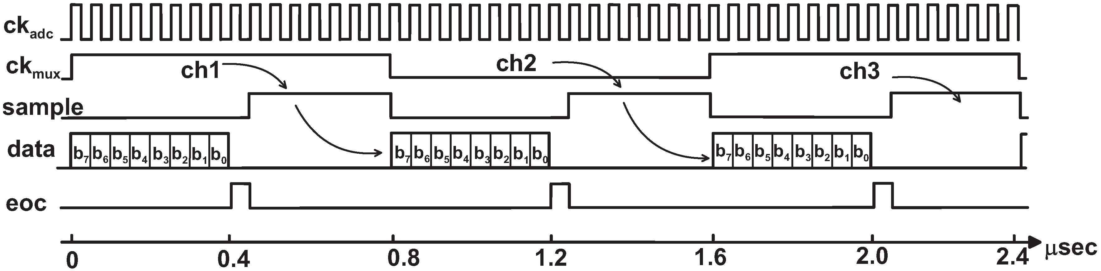
pF. kS/s per channel. Hence, a conversion period lasts 16 clock cycles (see Figure 5): The sampling phase lasts 7 clock periods to relax the specs of the input signal buffer, while every bit decision takes one clock period, starting from the most significant bit (MSB ). The last clock cycle is reserved for the end-of-count (EOC) operations. The current consumption of input buffer and A/D converter are 250 and 410 μA, respectively.
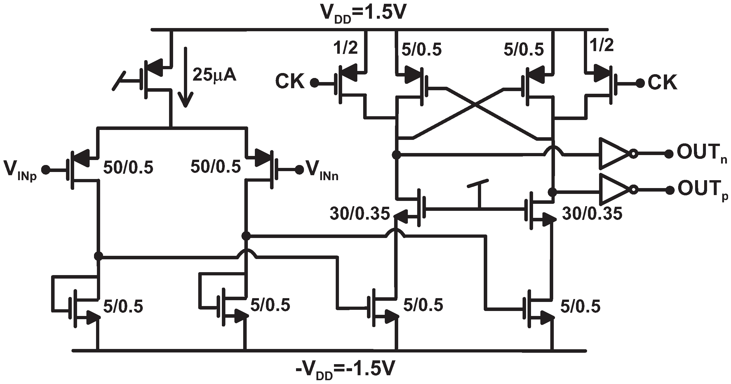
3.3. Digital Signal Processing
14000 ), these four thresholds correspond to an input-referred amplitude of ± 54 μV, ± 27 μV, ± 13 μV and ± 7 μV.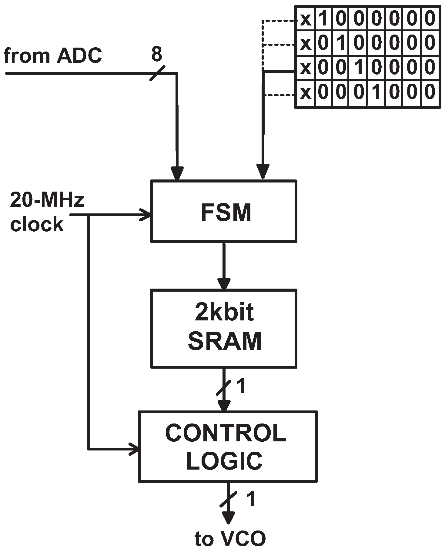

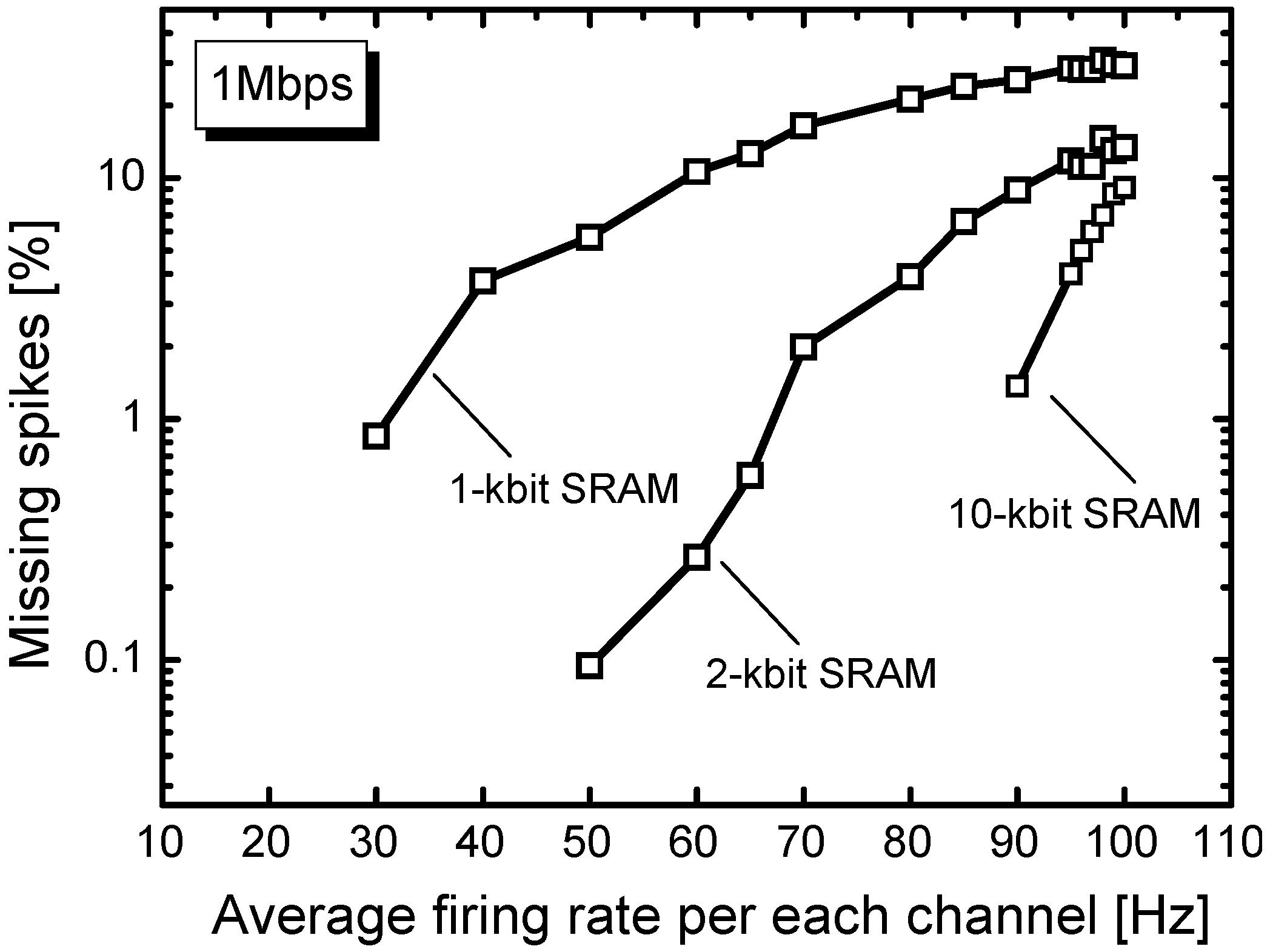
- • the lower the read speed, the higher the compression factor is; 1 Mbit/s read speed results in a compression factor of 10 (from 10.24 Mbit/s, corresponding to 64 channels sampled at 20 kHz per channel and 8 bit per sample, to 1.25 Mbit/s data rate) and allows saving a considerable amount of power and bandwidth at the transmitter side;
- • considering the worst-case scenario of 64 channels firing at 100 spike/s and 20 samples per spike with an 8 bit resolution, the average data throughput is about 1 Mbit/s.


| AP class | Original | Reduced | Peak-trough-width | |||
|---|---|---|---|---|---|---|
| Error type | I | II | I | II | I | II |
| A (379) | 4.1% | 6.9% | 3.1% | 2.9% | 23% | 22% |
| B (389) | 2.1% | 3.3% | 3.7% | 6.9% | 12% | 18% |
| C (401) | 6.2% | 5.5% | 6.9% | 6.0% | 17% | 30% |
3.4. Manchester-Coded FSK Modulator
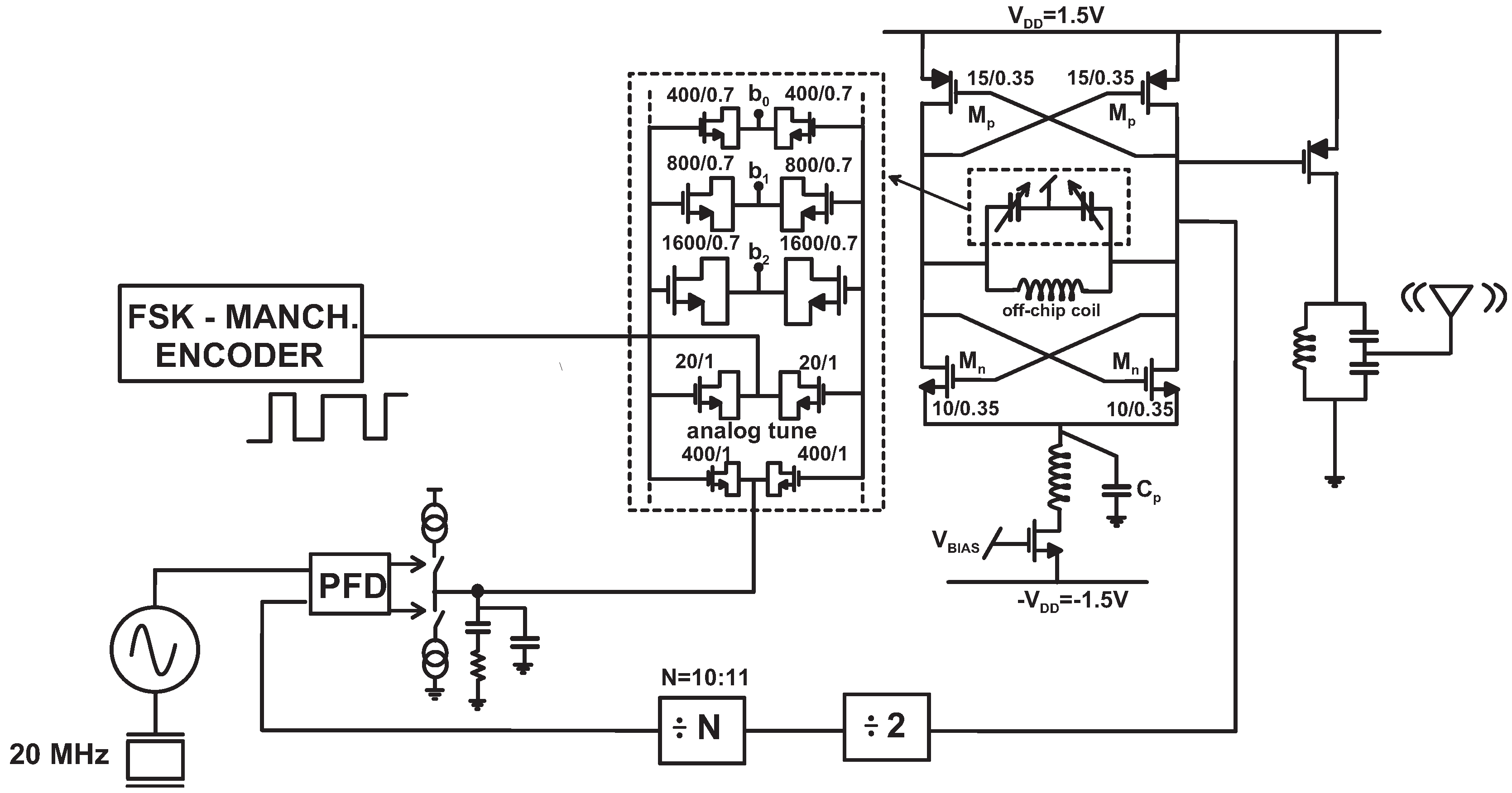

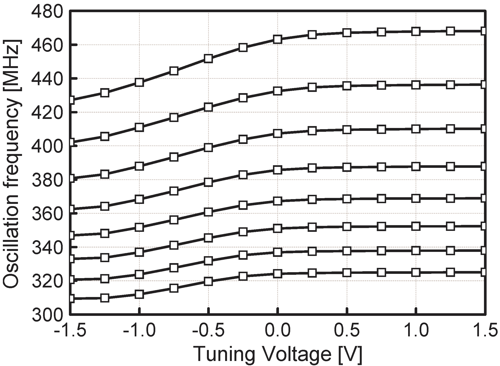
 the covered band of 80 MHz and C the tank capacitor. To make the oscillation frequency insensitive to the parasitic capacitance of the active devices, routing, pads and package pins (the inductor is off-chip), the tank capacitance has to be set in the pF range. Thus, we designed the oscillator with C tunable from 6 pF to 11 pF, determining an inductance value of about 20 nH. The tank capacitance is implemented by three digitally-controlled binary-weighted NMOS inversion-mode varactors that perform coarse tuning of the oscillation frequency and an analog NMOS inversion-mode varactor for fine-tuning of the frequency, enabling to close the loop of the PLL. Another small NMOS varactor is also adopted for frequency modulation.
- • The small-signal loop gain or excess gain [29] of the oscillator (gmRTANK, where gm is the small-signal transconductance of the double differential-pair and RTANK is the tank equivalent parallel resistance) has to be larger than 1 in order to assure the oscillation start-up. Since the common-mode output voltage of the oscillator is set to the half of the power supply to maximize the oscillation swing, i.e.,
![Jlpea 02 00211 i219]() V, we have:
V, we have:![Jlpea 02 00211 i220]() corresponding to a current larger than
corresponding to a current larger than![Jlpea 02 00211 i221]() μA. Note that in Equation (22) it was assumed that the overall transconductance gm of the double differential-pair is equal to the single MOS transconductance and that NMOS and PMOS transistors have the same overdrive voltage, Vov =
μA. Note that in Equation (22) it was assumed that the overall transconductance gm of the double differential-pair is equal to the single MOS transconductance and that NMOS and PMOS transistors have the same overdrive voltage, Vov = ![Jlpea 02 00211 i060]() =
= ![Jlpea 02 00211 i223]() V
V ![Jlpea 02 00211 i141]() 0.8 V.
0.8 V. - • The differential oscillation amplitude, A0, has to be sufficiently large (
![Jlpea 02 00211 i226]() 1.5 V) to drive the subsequent stages, i.e., the frequency dividers and the power amplify. Since
1.5 V) to drive the subsequent stages, i.e., the frequency dividers and the power amplify. Since![Jlpea 02 00211 i227]() where Q is the tank quality factor [30], the current IBIAS is minimized adopting an inductor with the maximum quality factor. We opted for an off-chip inductor of 21 nH featuring a Q of about 70 at 400 MHz. This choice results in a current larger than 320 μA to achieve the desired voltage amplitude.
where Q is the tank quality factor [30], the current IBIAS is minimized adopting an inductor with the maximum quality factor. We opted for an off-chip inductor of 21 nH featuring a Q of about 70 at 400 MHz. This choice results in a current larger than 320 μA to achieve the desired voltage amplitude. - • The VCO phase noise, which mainly determines the phase noise of the whole synthesizer at a frequency offset larger than the PLL loop bandwidth, has to be sufficiently lower in order not to worsen the Signal-to-Noise-Ratio (SNR ) of the modulated signal. This can be evaluated as Single-Sideband to Carrier Ratio, i.e., as the ratio of the power in a 1 Hz bandwidth at an offset
![Jlpea 02 00211 i232]() from the fundamental angular frequency
from the fundamental angular frequency ![Jlpea 02 00211 i233]() and the power of the carrier, giving [31]:
and the power of the carrier, giving [31]:![Jlpea 02 00211 i234]() where F is the noise factor of the transconductor (
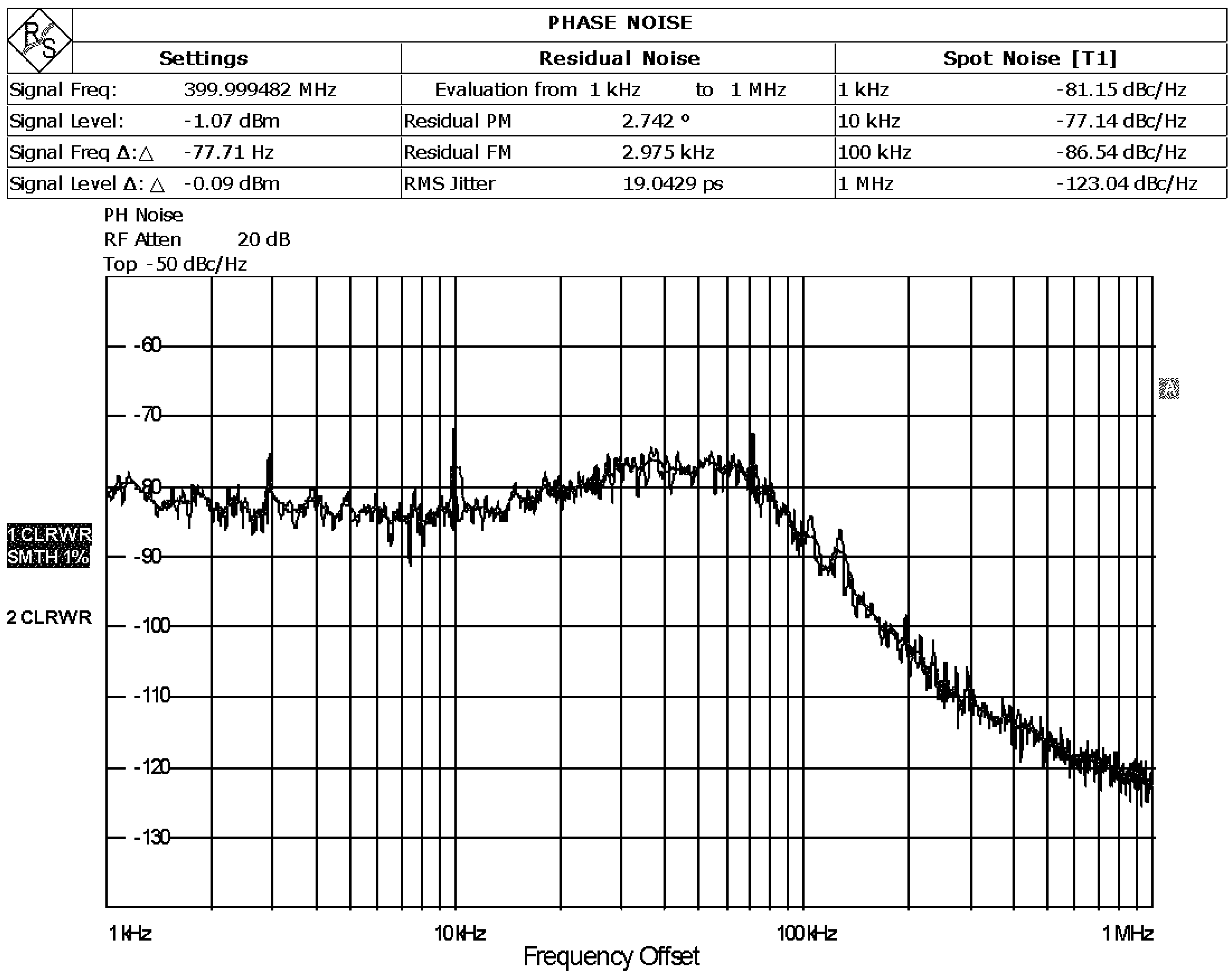
where F is the noise factor of the transconductor (![Jlpea 02 00211 i236]() ). From behavioral simulations, the phase noise at 1 MHz offset from the carrier has to be lower than –120 dBc/Hz to not to degrade the frequency modulated signal.
). From behavioral simulations, the phase noise at 1 MHz offset from the carrier has to be lower than –120 dBc/Hz to not to degrade the frequency modulated signal.


 μA, C in the 6–11 pF range and
  , the excess gain is approximately 2 and the oscillation amplitude is larger than 2 V, preventing the tail current generator to enter the ohmic region and avoiding a phase noise degradation. Moreover, these choices ensure that the phase noise is not an issue being better than 1–50 dBc/Hz at 1 MHz frequency offset.
 and fm are the peak frequency deviation (400 kHz) and the frequency modulation (1.25 MHz), respectively.
3.5. Power Amplifier
antenna via an off-chip resonant filter. The PA consists of an open-drain PMOS transistor directly connected to the oscillator output, sized in order to draw about 3.5 mA. Thus, the power delivered to the antenna is about 0 dBm considering a reasonable efficiency of 10%. The output power, and thus the power consumption of the PA, were set after estimating the sensitivity of the receiver, which depends on the modulation type, the signal bandwidth and the noise factor of the receiver itself. The receiver input noise in the signal bandwidth of 3 MHz is:
 is
is  dB [33]. Thus the input power needed at the receiver is:

 is the wavelength, and d is the distance between the antennas. While the receiver antenna is a dipole antenna and its gain can be estimated to be 0 dB, the transmitter antenna is a whip antenna with a gain that can be as low as –20 dB. Note that Equation (28) represents the power at the receiver antenna that is supposed to be matched with the receiver. Thus, the receiver input power is 3 dB lower. Thus, considering Equation (28) and setting the maximum transmission distance to 10 m, the power needed at the transmitter antenna is 11 dBm, where a 3 dB factor accounting for the matching between the receiver antenna and the receiver itself is considered. Finally, to have a safety margin, a PA featuring a 0 dBm output power was designed.
4. Experimental Results
4.1. Electrical Characterization
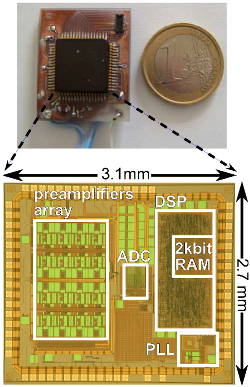
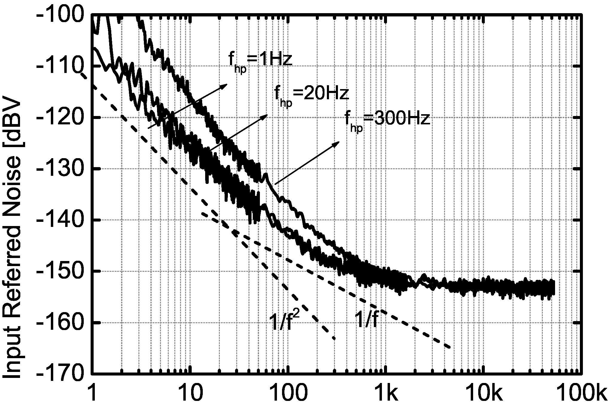
 mm2, pads included (see Figure 11). The preamplifier has a mid-band gain of about 65 dB, a high frequency cut-off of 10.5 kHz and a low-frequency cut-off tunable from 1 Hz to 1 kHz (see Figure 12). The input-referred noise, for Hz, is 3.05 μV, while the current consumption is 4 μA for the first stage, 0.001 μA and 0.3 μA for the
  high-pass filter and the second amplifying stage respectively, resulting in an overall NEF of 2.5. The input-referred power spectral density is shown in Figure 13 for different values of the GM -C filter high-pass corner frequency. The plateau of –152 dBV2 /Hz corresponds to an input-referred noise of about (25 nV)2 /Hz, close to the expected value. Note that, for Hz, the input-referred noise is mainly due to the GM -C high-pass filter, as predicted by Equation (14). The common-mode rejection ratio (CMRR ) and the power supply rejection ratio (PSRR ) of the overall pre-amplifier are higher than 65 dB and 50 dB, respectively, while the cross-talk between adjacent channels due to the analog multiplexing is lower than –40 dB.
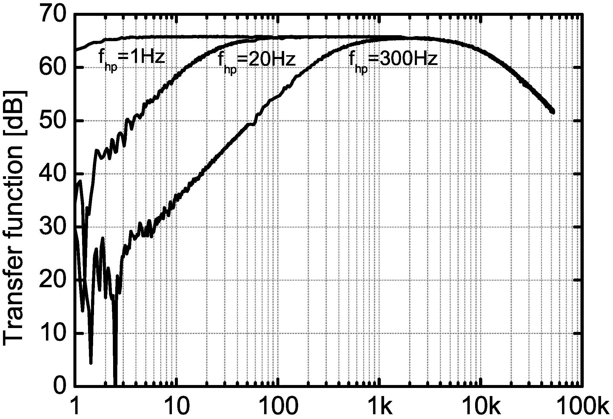


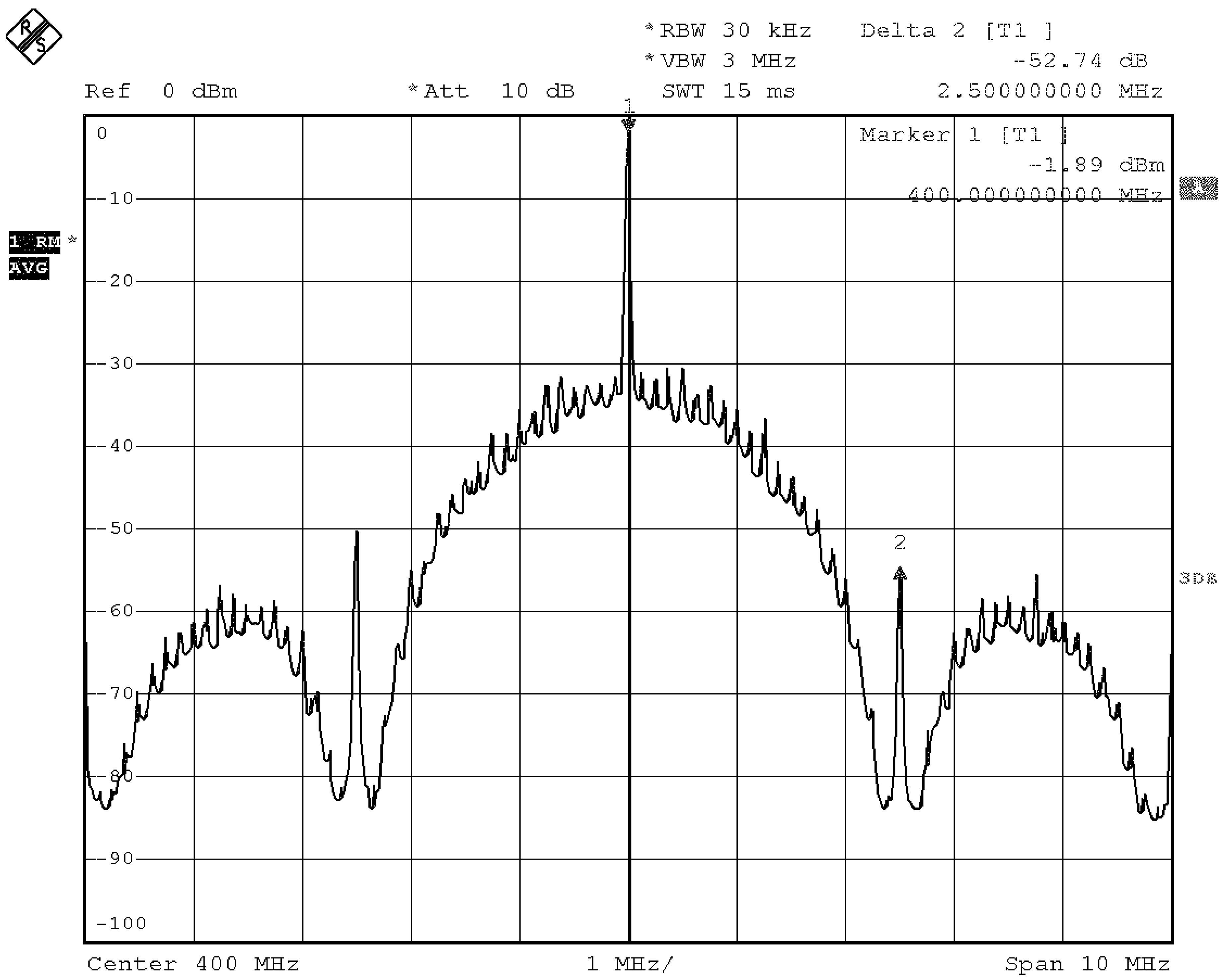
 whip antenna at the transmitter and a dipole antenna at the receiver side, the received power in a free space is shown in Figure 19. The sensitivity of the receiver has been measured to be –74 dBm for a BER of , close to the estimated theoretical value predicted by Equation (27) of –79 dBm, allowing a transmission range larger than 30 m. The system has also been successfully tested for a 10 m distance between transmitter and receiver in a hostile environment as a neuroscience laboratory, giving a PA efficiency of about 7% while delivering a –2 dBm at a 50- output load. Disabling the PA, the tank inductor may act as transmitting antenna; in such measurements about –70 dBm was received by a loop antenna placed at approximately 5 cm from the tank inductor.
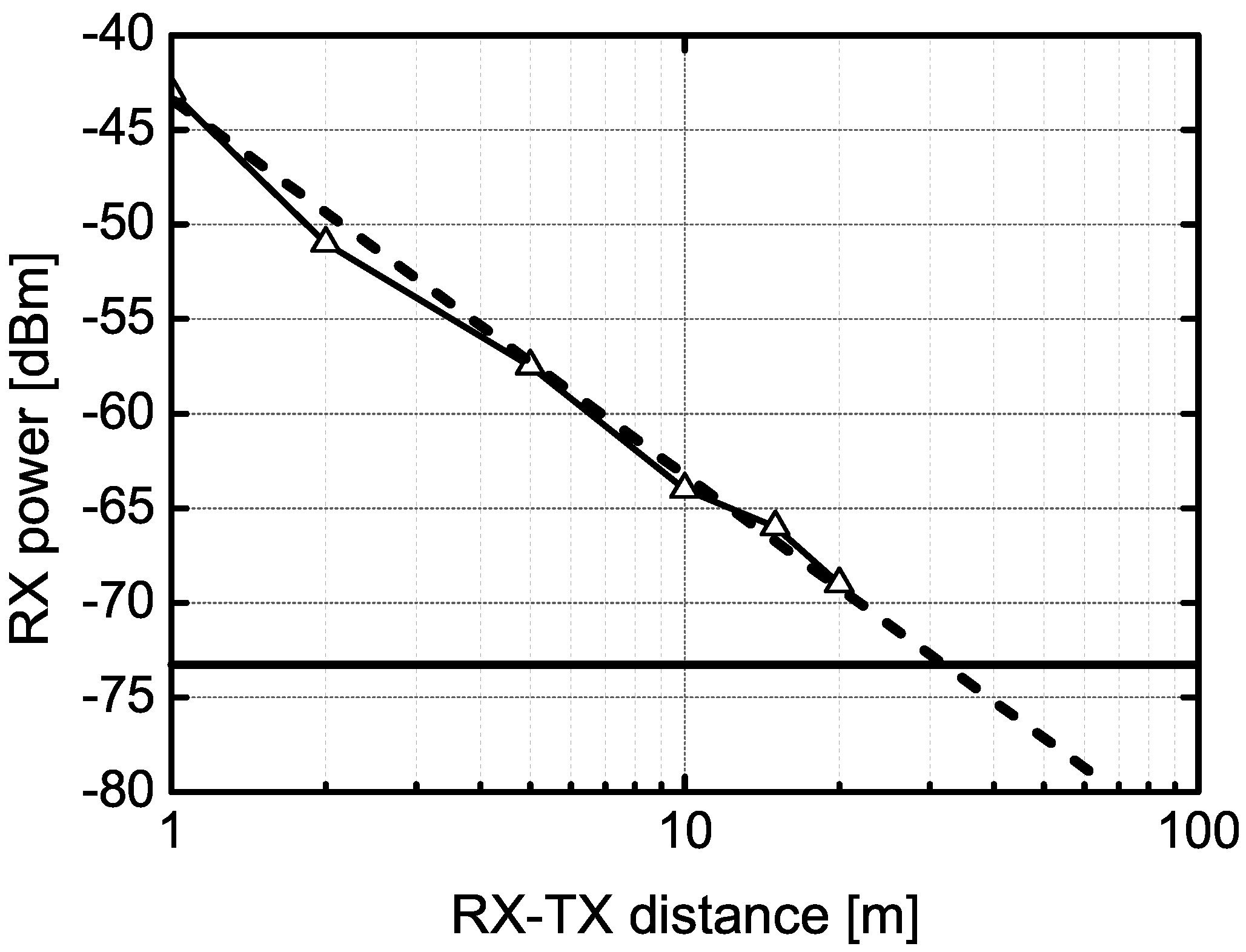
| Technology | 0.35 μm AMS |
| Supply Voltage | 3 V |
| Number of channels | 64 (16 available) |
| Pre-amplifier gain | 65 dB |
| Pre-amplifier band | HP tunable-10.5 kHz |
| Input-Referred Noise |   |
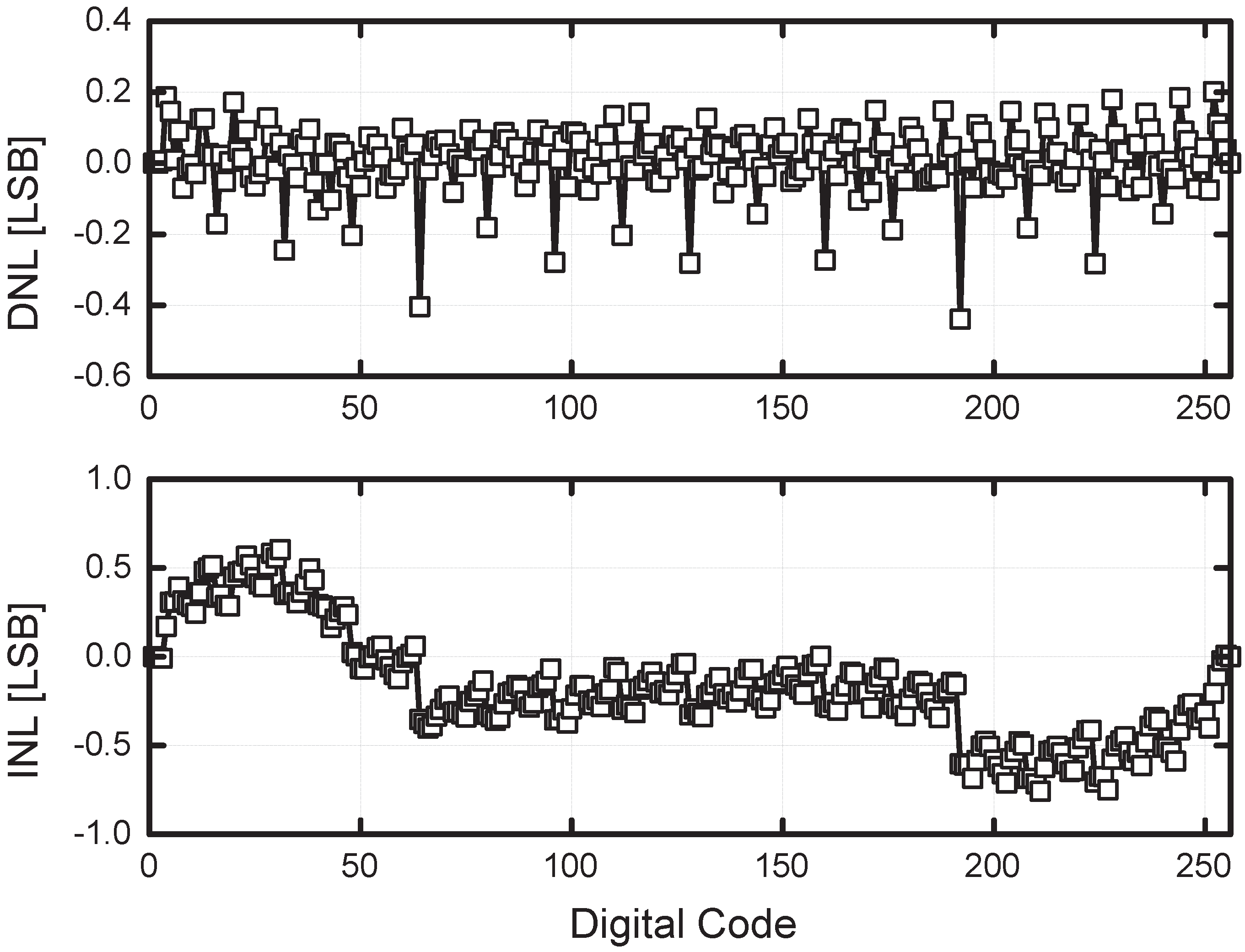
| ADC DNL-INL |  LSB; LSB;  LSB LSB |
| ADC ENOB | 7.2 |
| Transmission frequency | 400 MHz |
| Bit-rate | 1.25 Mbit/s |
| Current Consumption | |
| 20-MHz crystal oscillator | 90 μA |
| Pre-amplifiers |  A A |
| Line buffers |  A A |
| VGA | 50 μA |
| ADC buffer | 250 μA |
| ADC | 410 μA |
| DSP+2 kbit RAM | 400 μA |
| Modulator (PLL) | 700 μA |
| Power amplifier | 3.5 mA |
| Total power consumption | 6.7 mW (17.2 mW with PA enabled) |
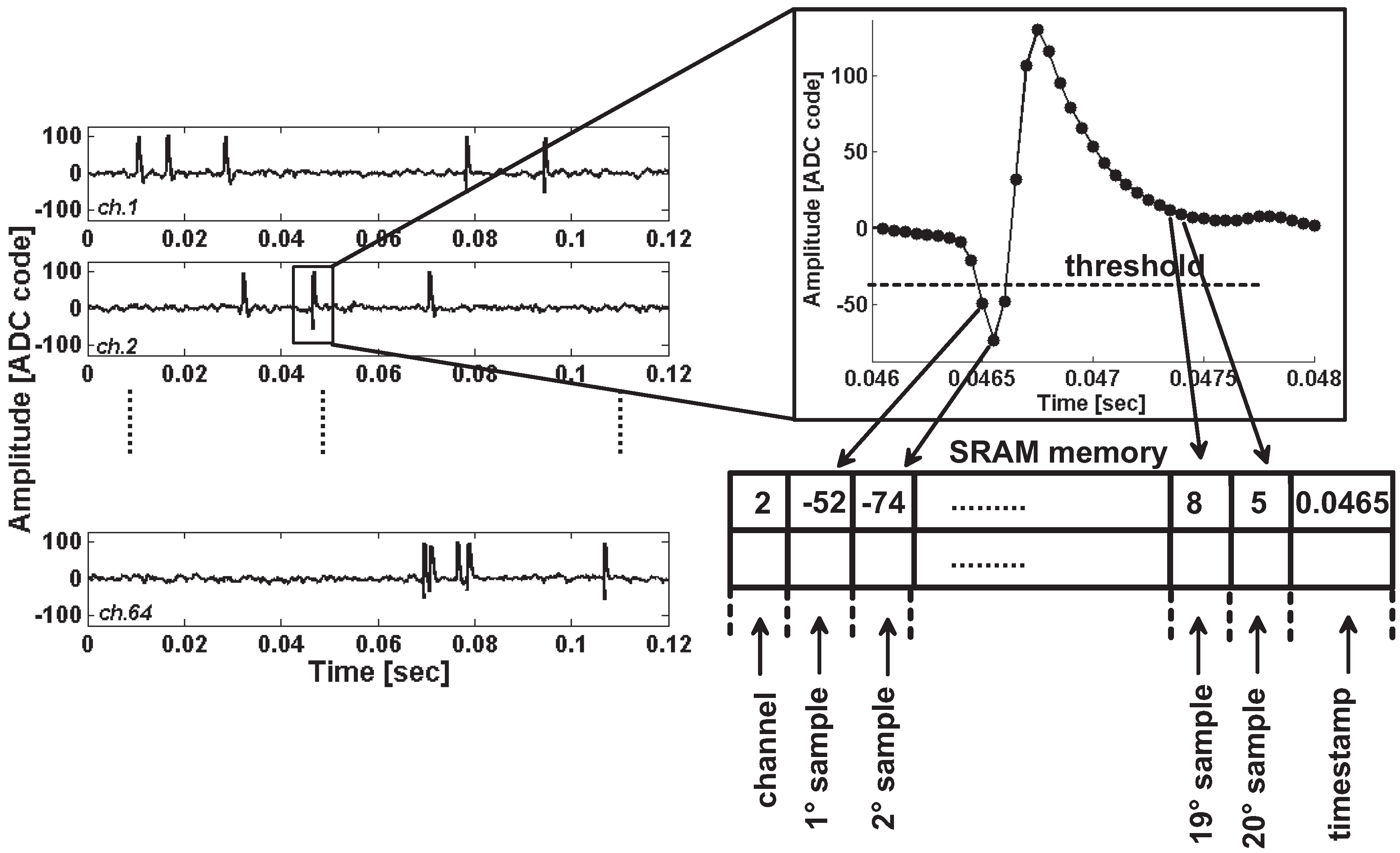
4.2. In Vivo Experiments
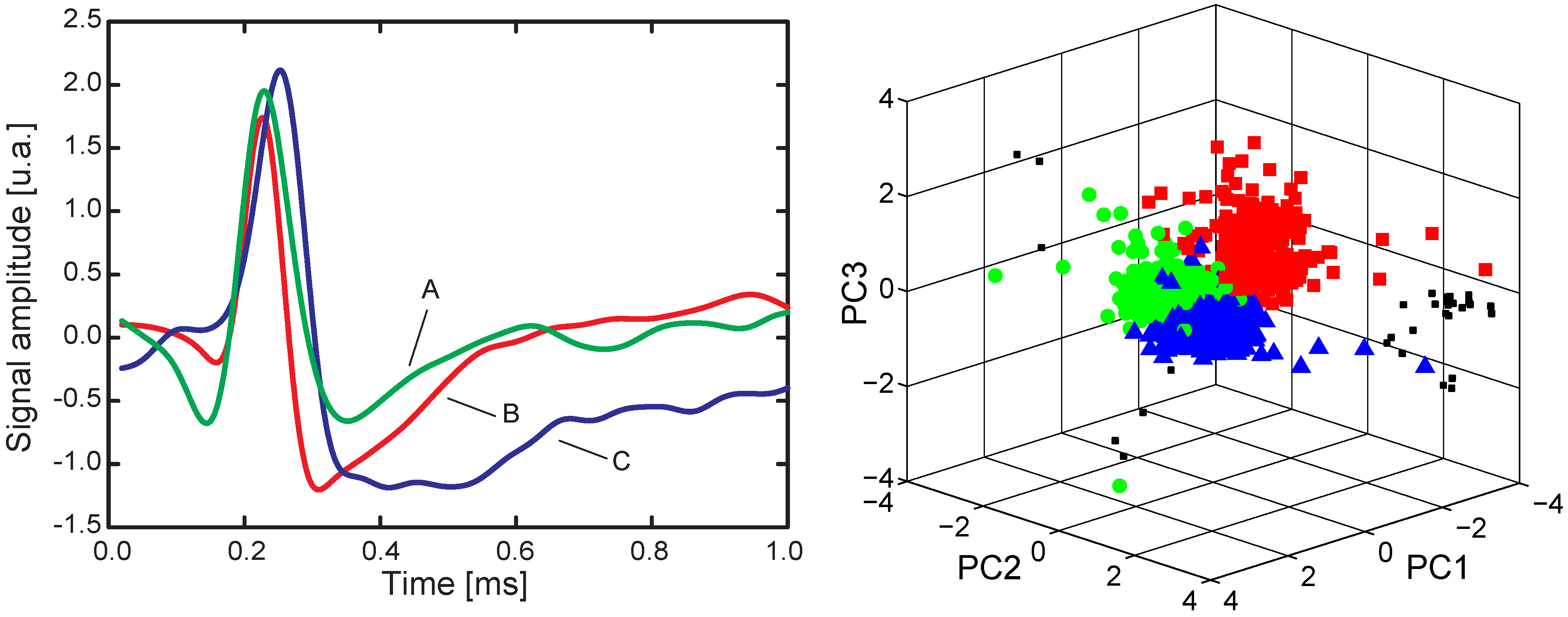
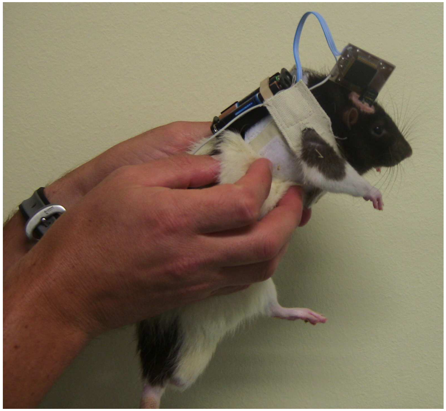
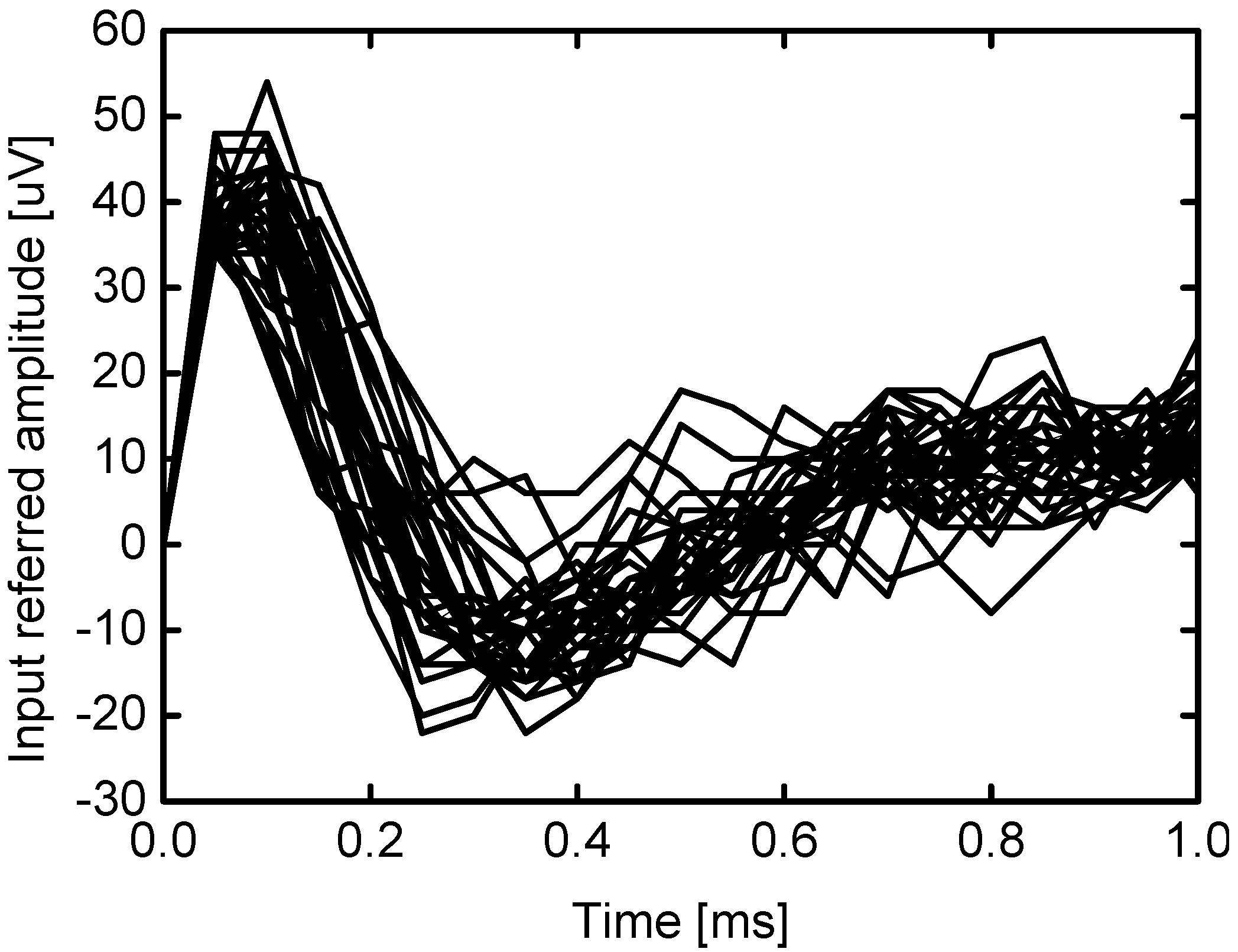
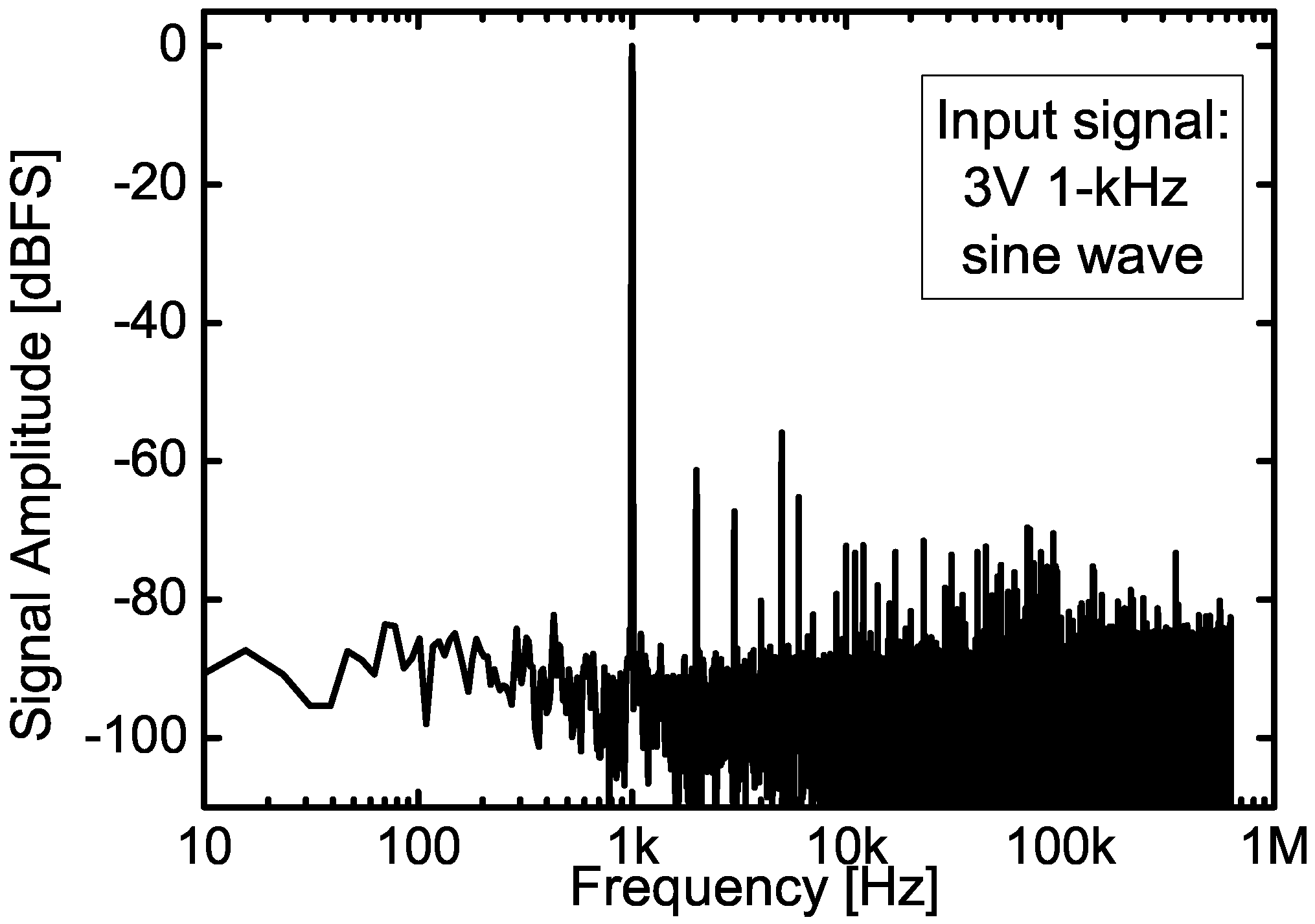
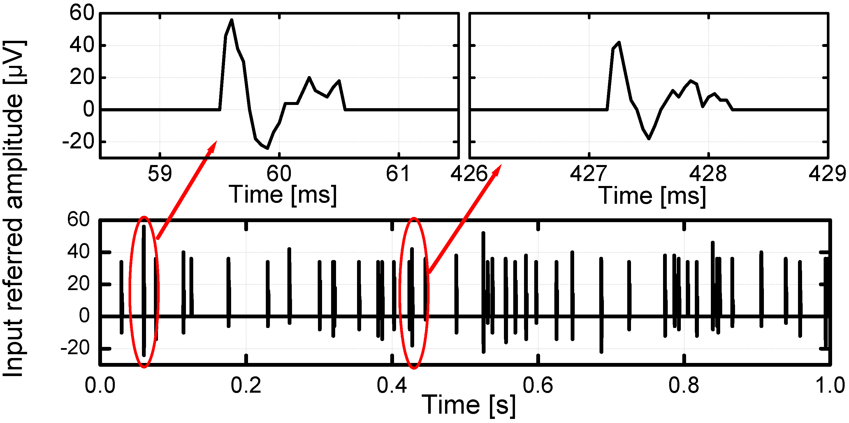
 cm2 and 4.5 g of weight) is directly connected to a 16 channel microelectrode array (Tucker-Davis), with an impedance in the 20–60 k range at 1 kHz, implanted into the somatosensory cortex of an adult rat. The board includes the packaged chip and 10 external small surface-mount components (0805 or 0603 footprint): the VCO inductor, the power-amplifier resonant filter components (2 capacitors and 1 inductor), the 20 MHz quartz, the PLL loop-filter (1 resistor and 2 capacitors) and 2 decoupling capacitors between power supplies. The antenna is a quarter-wavelength whip antenna: it consists of a piece of wire about 17 cm long, easily placed along the back of the rat. The backpack has a weight of 40 g and includes two AAA batteries with 1000 mA/h capacity that may allow neural activity recordings for more than 100 hours. The two batteries are connected via three 10 cm long wires to the headstage. At the beginning of the in vivo experiment, the quality of the signals from the implanted electrodes was analyzed using a commercial acquisition system by recording the raw signals and noise from the same 16 electrode channels. The recorded traces featured a noise of about 10 μVrms on all channels. The threshold of the digital peak processor was set to “x1000000 ” and the gain of the overall amplifying chain to the maximum value (83 dB) since the peak-to-peak spike amplitude was always lower than 100 μV. Thus, the digital threshold corresponds to an input-referred amplitude of about ±30 μV, i.e., ±3 times the rms noise. The high-pass cut-off frequency of the front-end amplifiers was set to about 300 Hz to properly reject the low-frequency signals and the power-line noise, enabling correct spike detection. The receiver dipole antenna has been placed at two meters from the rat while neural activity was recorded. Figure 21 shows a single trace recorded during the experiment and two spike waveforms extracted from the data stream, while in Figure 22 a large number of spikes recorded on the same channel are shown aligned in time.

5. Discussion and Conclusions
| Parameter | [3] | [6] | [7] | [35] | This work |
|---|---|---|---|---|---|
| Technology | 0.5 μm | 0.35 μm | 0.5 μm | 0.13 μm | 0.35 μm |
| Power source | inductive link | battery | battery | NA | battery |
| Number of channels | 100 | 128 | 32 | 64 | 64 (16 avail.) |
| Overall gain | 60 dB | 57–60 dB | 68–78 dB | 54–60 dB | 65–83 dB |
| Input noise | 5.1 μV | 4.9 μV | 9.3 μV | 6.5 μV | 3.05 μV |
| TX frequency | 433 MHz | 4 GHz | 915 MHz | 915 MHz | 400 MHz |
| Modulation | 2FSK | IR-UWB | 2FSK (PWM) | FSK-OOK | 2MC-FSK |
| Data type | spike detection | raw data | raw data | raw data | AP waveform |
| Data rate | 330 kbit/s | 90 Mbit/s | 640 kbaud/s | 1.5 Mbit/s | 1.25 Mbit/s |
| Bandwidth | 0.8 MHz | 1 GHz | 38 MHz | 3 MHz | 3 MHz |
| TX range | 13 cm |  1 m 1 m | 1m | 1 m | 30 m |
| Power per channel | 135 μW/ch | 47 μW/ch | 220 μW/ch | 80 μW/ch | 269 μW/ch |
 3 kS/s from all 64 channels. Higher sampling rates are possible only for a limited number of channels: assuming that 20 kS/s is the minimum sampling rate to acquire good quality neural signals, the maximum number of channels that can be recorded and transmitted simultaneously is only 9.
Acknowledgment
References and Notes
- Olsson, R.H.; Buhl, D.L.; Sirota, A.M.; Buzsaki, G.; Wise, K.D. Brain-machine interfaces: Past, present and future. Trends Neurosci. 2006, 29, 536–546. [Google Scholar] [CrossRef]
- Seese, T.; Harasaki, H.; Saidel, G.; Davies, C. Characterization of tissue morphology, angiogenesi, and temperature in the adaptive response of muscle tissue to chronic heating. Labs Invest. 1998, 78, 1553–1562. [Google Scholar]
- Harrison, R.R.; Watkins, P.T.; Lovejoy, R.O.; Kier, R.J.; Black, D.J.; Greger, B.; Solzbacher, F. A low-power integrated circuit for a wireless 100-electrode neural recording system. IEEE J. Solid State Circuits 2007, 1, 123–133. [Google Scholar]
- Sodagar, A.M.; Perlin, G.E.; Yao, Y.; Najafi, K.; Wise, K.D. An implantable 64-channel wireless microsystem for single-unit recording. IEEE J. Solid State Circuits 2009, 9, 2591–2604. [Google Scholar]
- Hochberg, L.R.; Serruya, M.D.; Friehs, G.M.; Mukand, J.A.; Saleh, M.; Caplan, A.H.; Branner, A.; Chen, D.; Penn, R.D.; Donoghue, J.P. Neuronal ensemble control of prosthetic devices by a human with tetraplegia. Nature 2006, 442, 164–171. [Google Scholar] [CrossRef]
- Chae, M.S.; Liu, W.; Yang, Z.; Chen, T.; Kim, J.; Sivaprakasam, M.; Yuce, M.A. 128-Channel 6 mW Wireless Neural Recording IC with On-the-Fly Spike Sorting and UWB Transmitter. In Proceedings of the IEEE International Solid-State Circuits Conference (ISSCC 2008), Digest of Technical Papers, San Francisco, CA, USA, 3–7 February 2008; pp. 146–148.
- Lee, S.B.; Lee, H.M.; Kiani, M.; Jow, U.M.; Ghovanloo, M. An inductively powered scalable 32-channel wireless neural recording system-on-a-chip for neuroscience applications. IEEE Trans. Biomed. Circuits Syst. 2010, 4, 360–371. [Google Scholar] [CrossRef]
- Liu, Y.-H.; Li, C.-H.; Lin, T.-H. A 200-pJ/b MUX-Based RF transmitter for implantable multichannel neural recording. IEEE Trans. Microw. Theory Tech. 2009, 57, 2533–2541. [Google Scholar] [CrossRef]
- Bonfanti, A.; Ceravolo, M.; Zambra, G.; Gusmeroli, R.; Borghi, T.; Spinelli, A.S.; Lacaita, A.L. A multi-channel low-power IC for neural spike recording with data compression and narrowband 400-MHz MC-FSK wireless transmission. In Proceedings of the 2010 European Solid-State Device Research Conference (ESSCIRC), Seville, Spain, 14–16 September 2010; pp. 330–333.
- Harrison, R.R.; Charles, C. An implantable 64-channel wireless microsystem for single-unit recording. IEEE J. Solid State Circuits 2003, 6, 958–965. [Google Scholar] [CrossRef]
- Cp is not drawn in Figure 3. It can be easily verified that these strays do not affect, in principle, the differential gain of the first stage. Only their mismatch causes a pole-zero doublet which, however, has no practical impact since it lays at very low frequency, below the band of interest.
- Vittoz, E.; Fellrath, J. CMOS analog integrated circuits based on weak inversion operations. IEEE J. Solid State Circuits 2003, 3, 224–231. [Google Scholar]
- Enz, C.C.; Krummenacher, F.; Vittoz, E.A. An analytical MOS transistor model valid in all region of operation and dedicated to low-voltage and low-current applications. Analog Integr. Circuits Signal Process. 1995, 8, 83–114. [Google Scholar] [CrossRef]
- Steyaert, M.S.J.; Sansen, W.M.C. A micropower low-noise monolithic instrumentation amplifier for medical purposes. IEEE J. Solid State Circuits 1987, 22, 1163–1168. [Google Scholar] [CrossRef]
- This limit can be overwhelmed adopting a current-reuse input stage that makes use of both NMOS and PMOS transistors [6,36]. However, in this case, the impact of flicker noise and of the input capacitance [see Equation (1)] may be detrimental.
- Chae, M.S.; Liu, W.; Sivaprakasam, M. Design Optimization for Integrated Neural Recording Systems. IEEE J. Solid State Circuits 2008, 49, 1931–1939. [Google Scholar]
- Mollazadeh, M.; Murari, K.; Cauwenberghs, G.; Thakor, N. From Spikes to EEG: Integrated Multichannel and Selective Acquisition of Neuropotentials. In Proceedings of the 30th Annual International Conference of the IEEE Engineering in Medicine and Biology Society (EMBS 2008), Vancouver, Canada, 20–25 August 2008; pp. 2741–2744.
- Joye, N.; Schmid, A.; Leblebici, Y. An electrical model of the cell-electrode interface for high-density microelectrode arrays. In Proceedings of the 30th Annual International Conference of the IEEE Engineering in Medicine and Biology Society (EMBS 2008), Vancouver, Canada, 20–25 August 2008; pp. 559–562.
- Agnes, A. Very low power Successive Approximation A/D Converter for Instrumentation Applications. Ph.D. Dissertation, Universitá di Pavia, Pavia, Italy, 2009. [Google Scholar]
- Razavi, B.; Wooley, B.A.; Leblebici, Y. Design techniques for high-speed, high-resolution comparators. IEEE J. Solid State Circuits 1992, 27, 1916–1926. [Google Scholar] [CrossRef]
- Figueiredo, P.M.; Vital, J.C. Kickback noise reduction techniques for CMOS latched comparators. IEEE Trans. Circuits Syst. II Express Briefs 2006, 53, 541–545. [Google Scholar] [CrossRef]
- Vibert, J.F.; Costa, J. Spike separation in multiunit records: a multivariate analysis of spike descriptive parameters. Electroenceophal. Clin. Neurophys. 1979, 47, 172–182. [Google Scholar] [CrossRef]
- Oweiss, K. A Systems Approach for Data Compression and Latency Reduction in Cortically Controlled Brain Machine Interfaces. IEEE Trans. Biomed. Eng. 2006, 53, 1364–1377. [Google Scholar] [CrossRef]
- Lewicki, M.S. A review of methods for spike sorting: The detection and classification of neural action potentials. Comput. Meth. Prog. Biomed. 1998, 9, 53–78. [Google Scholar]
- Zouridakis, G.; Tam, D.C. Identification of reliable spike templates in multi-unit extracellular recordings using fuzzy clustering. Comput. Meth. Prog. Biomed. 2000, 61, 91–98. [Google Scholar] [CrossRef]
- The public database is available at Professor Rodrigo Quiroga’s website, http://www2.le.ac.uk/departments/engineering/research/bioengineering/neuroengineering-lab/spike-sorting/ [37]. The file adopted to validate the compression algorithm is C-difficult1-noise01.mat.
- Bonfanti, A.; Borghi, T.; Gusmeroli, R.; Zambra, G.; Oliyink, A.; Fadiga, L.; Spinelli, A.S.; Baranauskas, G. A low-power integrated circuit for analog spike detection and sorting in neural prosthesis systems. In Proceedings of the IEEE Biomedical Circuits and Systems Conference (BioCAS 2008), Baltimore, MD, USA, 20–22 November 2008; pp. 257–260.
- Andreani, P.; Fard, A. More on the
![Jlpea 02 00211 i040]() Phase Noise Performance of CMOS Differential-Pair LC-Tank Oscillators. IEEE J. Solid State Circuits 2006, 41, 2703–2712. [Google Scholar] [CrossRef]
Phase Noise Performance of CMOS Differential-Pair LC-Tank Oscillators. IEEE J. Solid State Circuits 2006, 41, 2703–2712. [Google Scholar] [CrossRef] - Bonfanti, A.; Pepe, F.; Samori, C.; Lacaita, A.L. Flicker noise up-conversion due to harmonic distortion in Van der Pol oscillators. IEEE Trans. Circuit Syst. I 2012, 59, 1418–1430. [Google Scholar] [CrossRef]
- The quality factor of the tank is approximately determined by the inductor loss at 400 MHz frequency, giving
![Jlpea 02 00211 i239]() .
. - Samori, C.; Lacaita, A.L.; Villa, F.; Zappa, F. Spectrum folding and phase noise in LC tuned oscillators. IEEE Trans. Circuit Syst. I 1998, 45, 781–790. [Google Scholar]
- Carson, J.R. Notes on the theory of modulation. Proc. Inst. Radio Eng. 1922, 10, 57–64. [Google Scholar] [CrossRef]
- Tan, C.; Tjhung, T.; Singh, H. Performance of Narrow-Band Manchester Coded FSK with Discriminator Detection. IEEE Trans. Commun. 1983, 31, 659–667. [Google Scholar] [CrossRef]
- Lacaita, A.; Levantino, S.; Samori, C. Integrated Frequency Synthesizers for Wireless Systems; Cambridge University Press: Cambridge, UK, 2007. [Google Scholar]
- Abdhelhalim, K.; Genov, R. 915-MHz Wireless 64-Channel Neural Recording SoC with Programmable Mixed-Signal FIR Filters. In Proceedings of the 2011 European Solid-State Device Research Conference (ESSCIRC), Helsinki, Finland, 12–16 September 2011; pp. 223–226.
- Liew, W.-S.; Zou, X.; Lian, Y. A 0.5-V 1.13-μW/channel neural recording interface with digital multiplexing scheme. In Proceedings of the 2011 European Solid-State Device Research Conference (ESSCIRC), Helsinki, Finland, 12–16 September 2011; pp. 219–222.
- Martinez, J.; Pedreira, C.; Ison, M.J.; Quiroga, R.Q. Realistic simulation of extracellular recordings. J. Neurosci. Meth. 2009, 184, 285–293. [Google Scholar]
© 2012 by the authors; licensee MDPI, Basel, Switzerland. This article is an open access article distributed under the terms and conditions of the Creative Commons Attribution license (http://creativecommons.org/licenses/by/3.0/).
Share and Cite
Bonfanti, A.; Ceravolo, M.; Zambra, G.; Gusmeroli, R.; Baranauskas, G.; Angotzi, G.N.; Vato, A.; Maggiolini, E.; Semprini, M.; Spinelli, A.S.; et al. A Multi-Channel Low-Power System-on-Chip for in Vivo Recording and Wireless Transmission of Neural Spikes. J. Low Power Electron. Appl. 2012, 2, 211-241. https://doi.org/10.3390/jlpea2040211
Bonfanti A, Ceravolo M, Zambra G, Gusmeroli R, Baranauskas G, Angotzi GN, Vato A, Maggiolini E, Semprini M, Spinelli AS, et al. A Multi-Channel Low-Power System-on-Chip for in Vivo Recording and Wireless Transmission of Neural Spikes. Journal of Low Power Electronics and Applications. 2012; 2(4):211-241. https://doi.org/10.3390/jlpea2040211
Chicago/Turabian StyleBonfanti, Andrea, Maria Ceravolo, Guido Zambra, Riccardo Gusmeroli, Gytis Baranauskas, Gian Nicola Angotzi, Alessandro Vato, Emma Maggiolini, Marianna Semprini, Alessandro Sottocornola Spinelli, and et al. 2012. "A Multi-Channel Low-Power System-on-Chip for in Vivo Recording and Wireless Transmission of Neural Spikes" Journal of Low Power Electronics and Applications 2, no. 4: 211-241. https://doi.org/10.3390/jlpea2040211
APA StyleBonfanti, A., Ceravolo, M., Zambra, G., Gusmeroli, R., Baranauskas, G., Angotzi, G. N., Vato, A., Maggiolini, E., Semprini, M., Spinelli, A. S., & Lacaita, A. L. (2012). A Multi-Channel Low-Power System-on-Chip for in Vivo Recording and Wireless Transmission of Neural Spikes. Journal of Low Power Electronics and Applications, 2(4), 211-241. https://doi.org/10.3390/jlpea2040211