1. Introduction
A resonator is the core device for generating a time–frequency signal, which is the reference for applications such as sensing, positioning, navigation, etc. It is also the “heart” of all electronic systems, in which the stability of the output frequency signals affects the overall system performance [
1]. The traditional quartz resonator, with a large size and low accuracy, is very difficult to integrate, becoming one of the bottlenecks limiting the miniaturization of the system and its performance. The silicon MEMS resonator shows much better benefits than those of traditional quartz ones [
2]. The silicon MEMS resonator is more than ten times smaller than the traditional quartz resonator [
3] and can be integrated with CMOS chips [
4], thus bringing disruptive innovations in the related fields [
5].
The PLL (phase-locked loop) is an electronic circuit. Its operation principle is based on the comparison of the phase of the reference clock with the phase of the feedback clock signal to achieve a zero-phase output, thus achieving the purpose of phase locking [
6]. The PLL is often used as a frequency multiplier, modulation and demodulation circuits, and is always used to generate a clock signal in digital systems [
7]. In the clock reference system, the PLL is a key module to help the MEMS resonator realize an efficient and complete clock output [
8]. For the MEMS-based resonator, the PLL can be connected to the back stage of the resonator output to process its frequency.
The mechanism by which phase-locked loops (PLLs) enhance the long-term stability of reference clocks can be analyzed through three key aspects: closed-loop control characteristics, noise suppression capabilities, and environmental adaptability.
The PLL continuously monitors the phase error between the local oscillator (LO) output and a high-stability external reference source using a phase detector [
6,
8]. This error signal, proportional to the phase difference, is converted into a corrective voltage through the loop filter, which drives the voltage-controlled oscillator (VCO) to adjust its output frequency. The dynamic behavior of this process is described by a second-order linearized model:
where
is the damping coefficient and
is the natural frequency. By optimizing the loop bandwidth, the PLL effectively suppresses low-frequency phase noise from the LO while tracking the long-term frequency drift of the external reference. PLLs employ multi-mode compensation mechanisms to mitigate environmental disturbances, such as temperature fluctuations and power supply variations. For temperature compensation, high-precision sensors integrated into the LO module collect real-time temperature data. These data are combined with pre-stored frequency–temperature characteristics (typically modeled as polynomials) in a lookup table (LUT) to generate a feedforward compensation voltage, which is superimposed onto the VCO control input. This approach significantly reduces thermally induced frequency drift. In 5G base stations, dual-reference PLL architectures (primary GPS + backup IEEE 1588) achieve inter-base station synchronization errors below ±50 ns when locked to GPS 1PPS signals. During GPS outages, the holdover mode maintains synchronization accuracy within ±100 ns over 24 h, complying with the stringent 3GPP TS 38.104 requirement (<1.5 μs) for TDD air interface synchronization. NASA’s Deep Space Atomic Clock (DSAC) project integrates a miniaturized cesium beam atomic clock with a wide-capture-range PLL, achieving a daily stability of 3 × 10
−15 under extreme conditions (−40 °C to +70 °C and high radiation). This enables sub-meter ranging accuracy for deep-space missions. These examples demonstrate that PLLs, through the integration of high-stability references and adaptive compensation algorithms, have become a cornerstone technology for enhancing long-term clock stability in mission-critical systems.
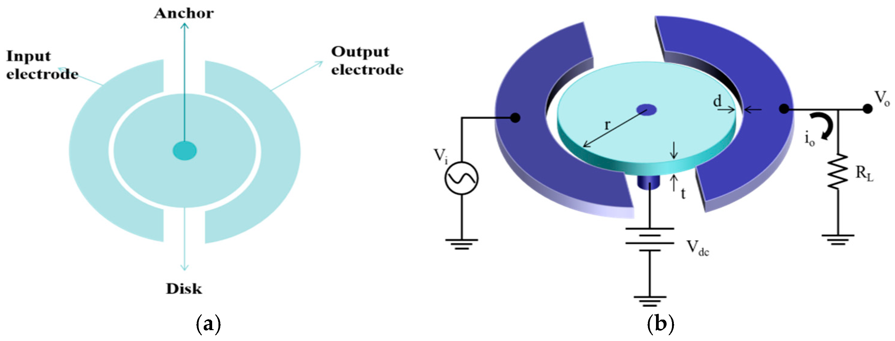
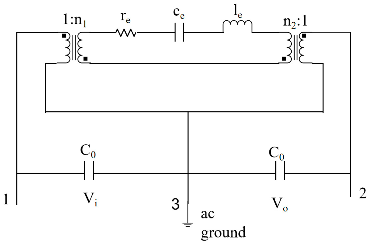
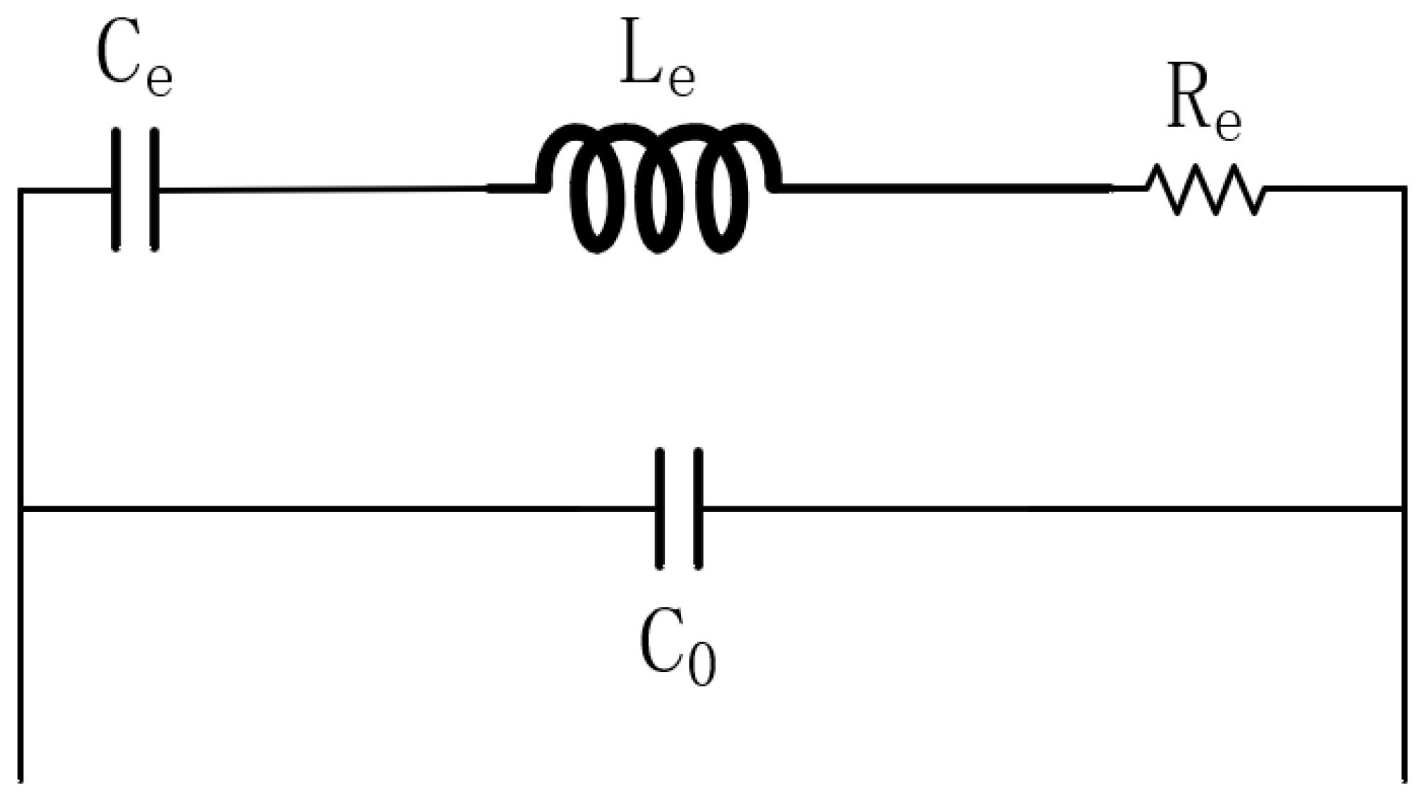
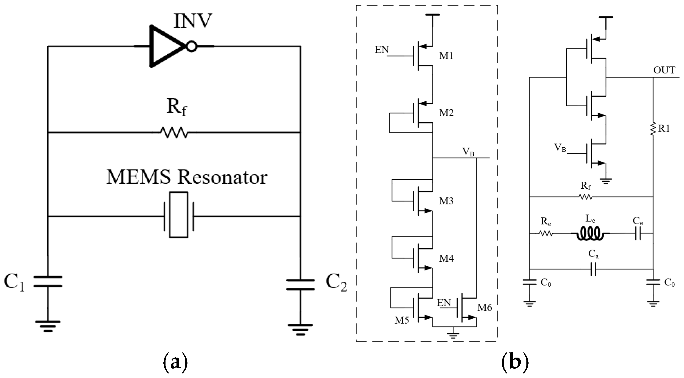
In this paper, firstly, a capacitive disk MEMS resonator is designed. The mechanical modeling of the resonator is mapped to the electrical modeling according to the electromechanical mapping rules to obtain a macro-equivalent resonator electrical model. Secondly, a Pierce oscillator circuit is designed to generate a clock reference signal. Subsequently, a charge pump PLL is designed to connect to the back stage of the oscillator circuit to process its frequency.
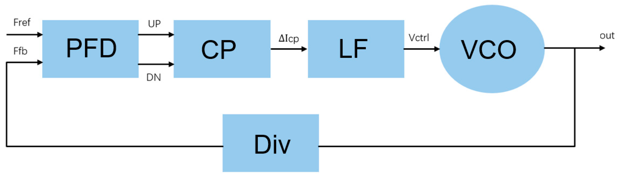
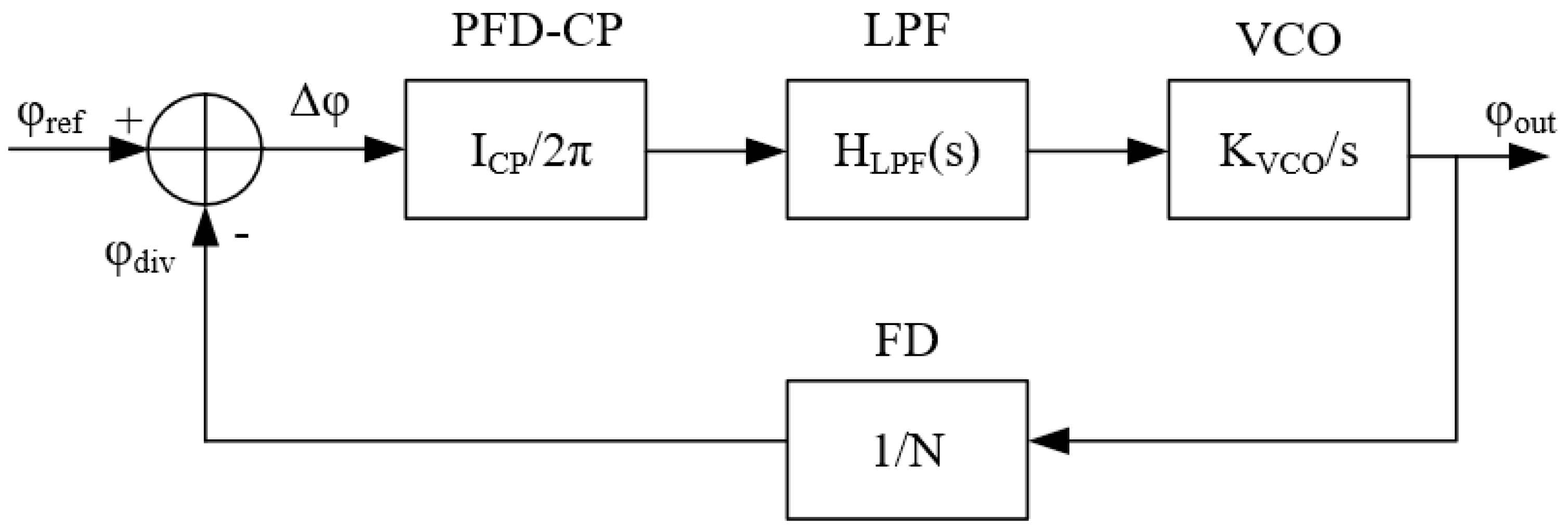
3. Charge Pump Phase-Locked Loop
In the MEMS-based resonator, a phase-locked loop can be connected to the back stage of the resonator’s output to condition its frequency. The PLL is a key module to help the MEMS resonator achieve an efficient and complete clock reference. The basic model of the PLL consists of an LF (loop filter), a VCO (voltage-controlled oscillator), a PFD (phase frequency detector), a CP (charge pump), and a divider. These four components form a closed-loop control to lock the phase of the input signals. The PLL is often used as a multiplier, modulator, and demodulator to generate clock signals in communication systems [
15]. These four components construct a closed-loop control to lock the phase of the input signal [
16].
Figure 6 shows the block diagram of a phase-locked loop of a charge pump.
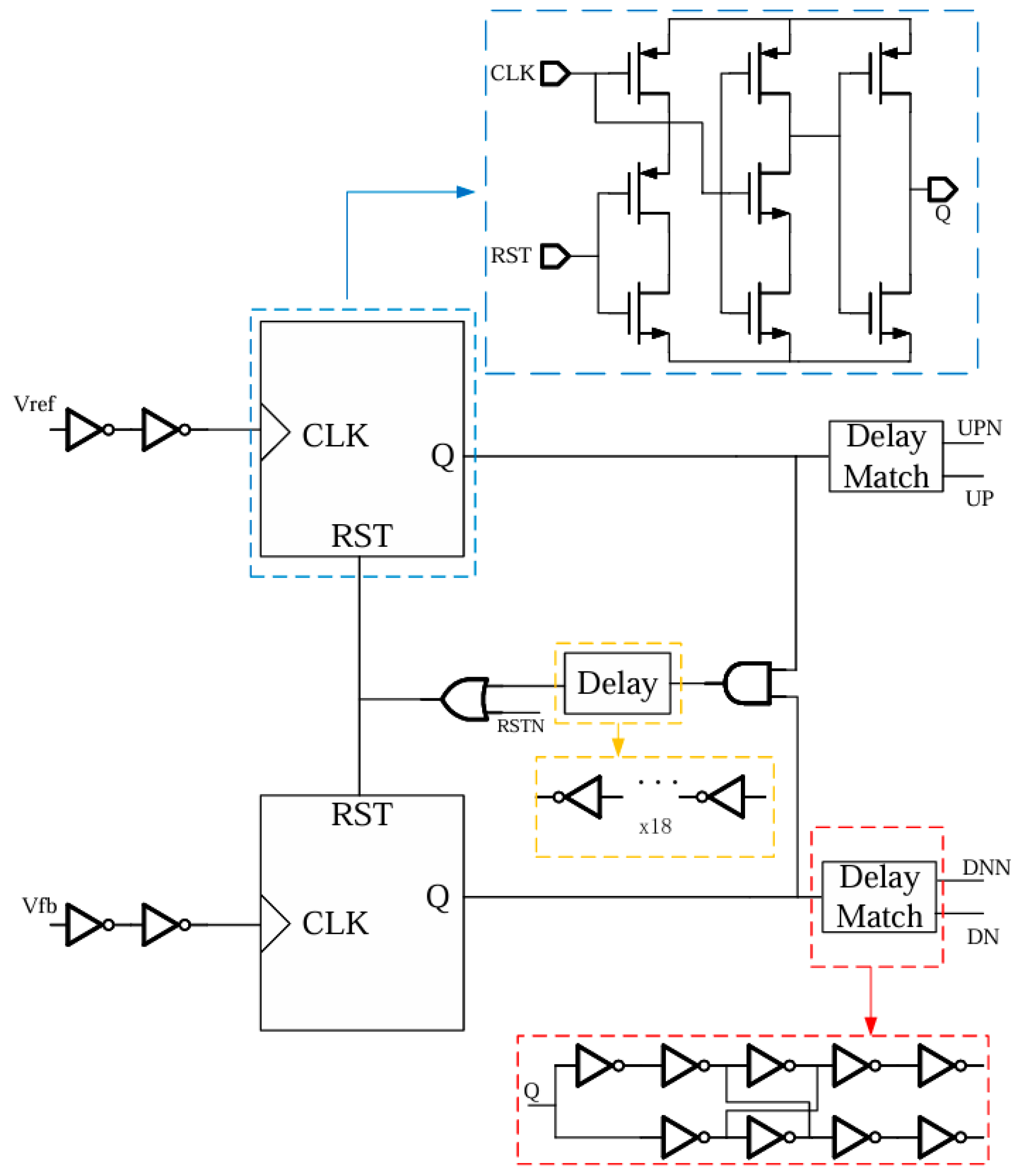
The frequency discriminator is an important module in the charge pump phase-locked loop (CPPLL), which realizes the output of charging and discharging pulse signals by comparing the frequency and phase of the reference signal and the crossover signal in the PLL.
Figure 7 shows the circuit structure schematic diagram of the frequency discriminator used in this paper. The frequency discriminator is mainly composed of two TSPC (true single-phase clock) structures; the input reference signal Fref and the feedback input signal Fdiv are connected to the CLK signal terminal of the TSPC structure in the figure, and the output signals are the UP signal and the DN signal, respectively, which are used as inputs to the two reset terminals of the TSPC structure through an output signal after a gate, and the output signals are used as inputs to the two reset terminals of the TSPC structure.
Since the output of the PFD is a digital signal of the phase difference, it cannot directly control the VCO, so the charge pump module is introduced. The main function of the charge pump is to use the digital signal output from the PFD as a switch to control the positive and negative currents and to charge and discharge the capacitors in the loop low-pass filter at the later stage so as to convert the output signal of the PFD into a variable voltage signal and to modulate the frequency of the VCO. In this design, a source level switched charge pump with a common source and common gate and operational amplifier is used, and the circuit results are shown in
Figure 8.
The simulation study of the charge pump circuit focused on the current matching characteristics between its charging and discharging branches. A DC sweep analysis was conducted by scanning the output voltage
vcpout from 0 V to 1.2 V, with a detailed investigation of the current deviation between the charging current
Iup and discharging current
Idn within the operational range of 0.2 V to 1 V. The simulation results, presented in
Figure 8b, reveal that, across the output voltage range of 0–1.1 V, the relative current mismatch ratio—defined as the difference between
Iup and
Idn normalized to their average magnitude—measures approximately 0.026%. This quantifies the exceptional charge/discharge current matching performance of the proposed charge pump design, demonstrating its capability to maintain balanced current symmetry under varying output conditions. The sub-0.03% mismatch ratio validates the effectiveness of the circuit topology in minimizing systematic errors inherent to conventional charge pump architectures.
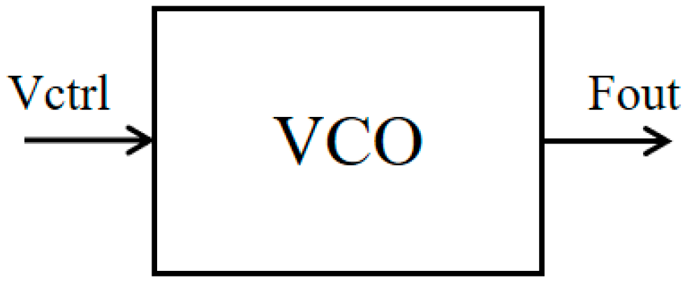
The voltage-controlled oscillator, as a module of the charge pump phase-locked loop to generate the output signal, is shown in
Figure 9, and its output, the frequency of the signal Fout, is controlled by the output voltage Vctrl of the previous loop filter circuit.
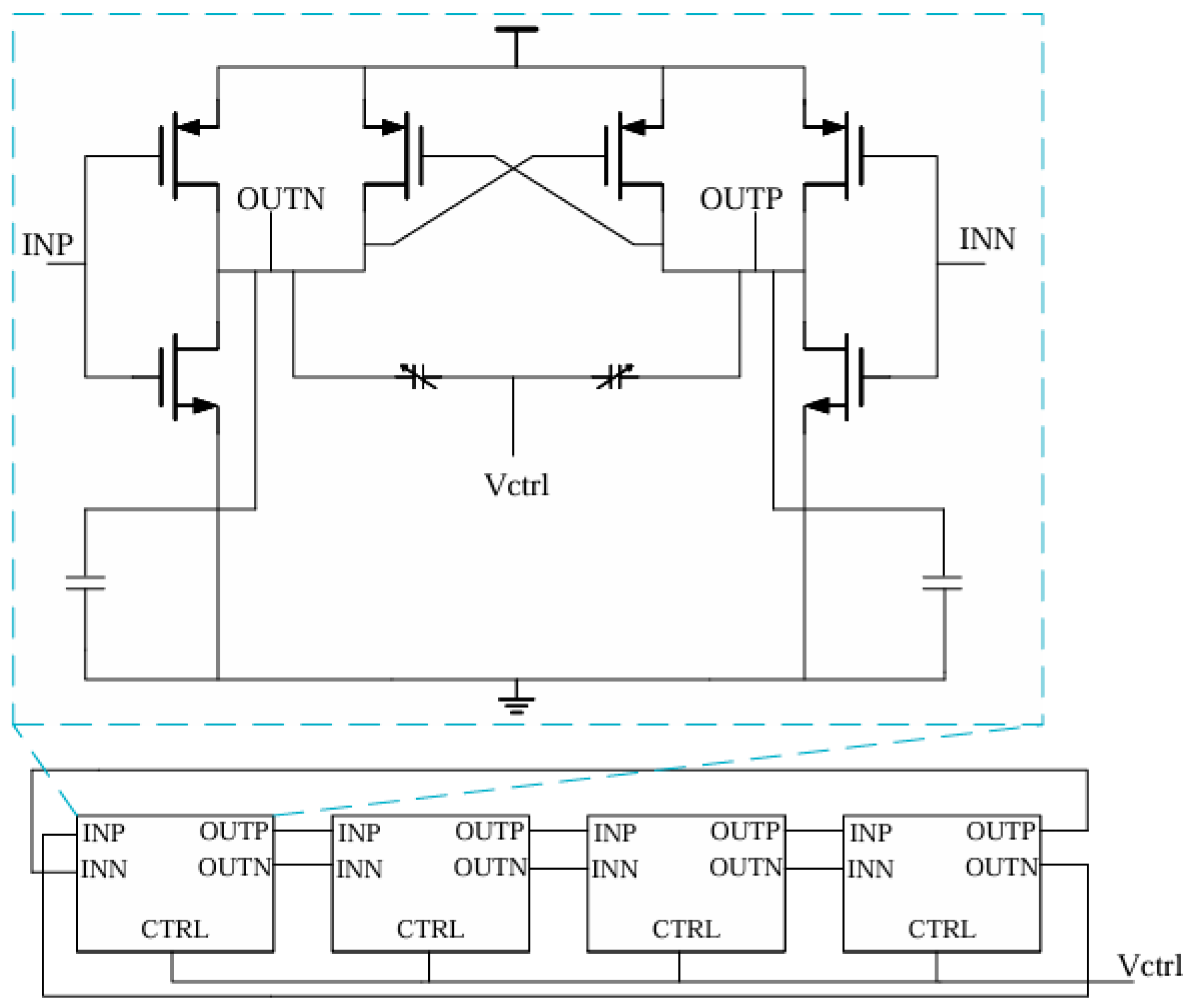
The voltage-controlled oscillator designed in this paper adopts a differential annular voltage-controlled oscillator structure, and the specific circuit is shown in
Figure 10.
Figure 11 shows the frequency sweep simulation and the phase noise simulation results of the voltage-controlled oscillator. According to the simulation diagram, the lowest frequency is 695 MHz, and the highest frequency is 1 GHz, that is, the tuning range of the signal frequency is 695 MH–1 GHz, and the linearity of the voltage-controlled oscillator in this paper is good. The phase noise is −98.7 dBc/Hz@1 MHz, and the voltage-controlled oscillator circuit designed in this paper has good noise performance.
In charge pump phase-locked loops, the frequency of the voltage-controlled oscillator output signal Fout is significantly higher than that of the reference signal Fref. Consequently, a frequency divider is employed to down-divide Fout. The divider circuit operates by reducing the frequency of the VCO’s high-speed clock signal and feeding the divided signal back to the phase-frequency detector. This feedback loop continuously adjusts the VCO frequency until the phase difference between the divided clock and the reference clock converges to zero, achieving a phase lock in the PLL system. The closed-loop mechanism ensures precise frequency synchronization through iterative error correction, where the divider ratio directly determines the final locked frequency relationship Fout = N⋅Fref, with N representing the programmable division factor.
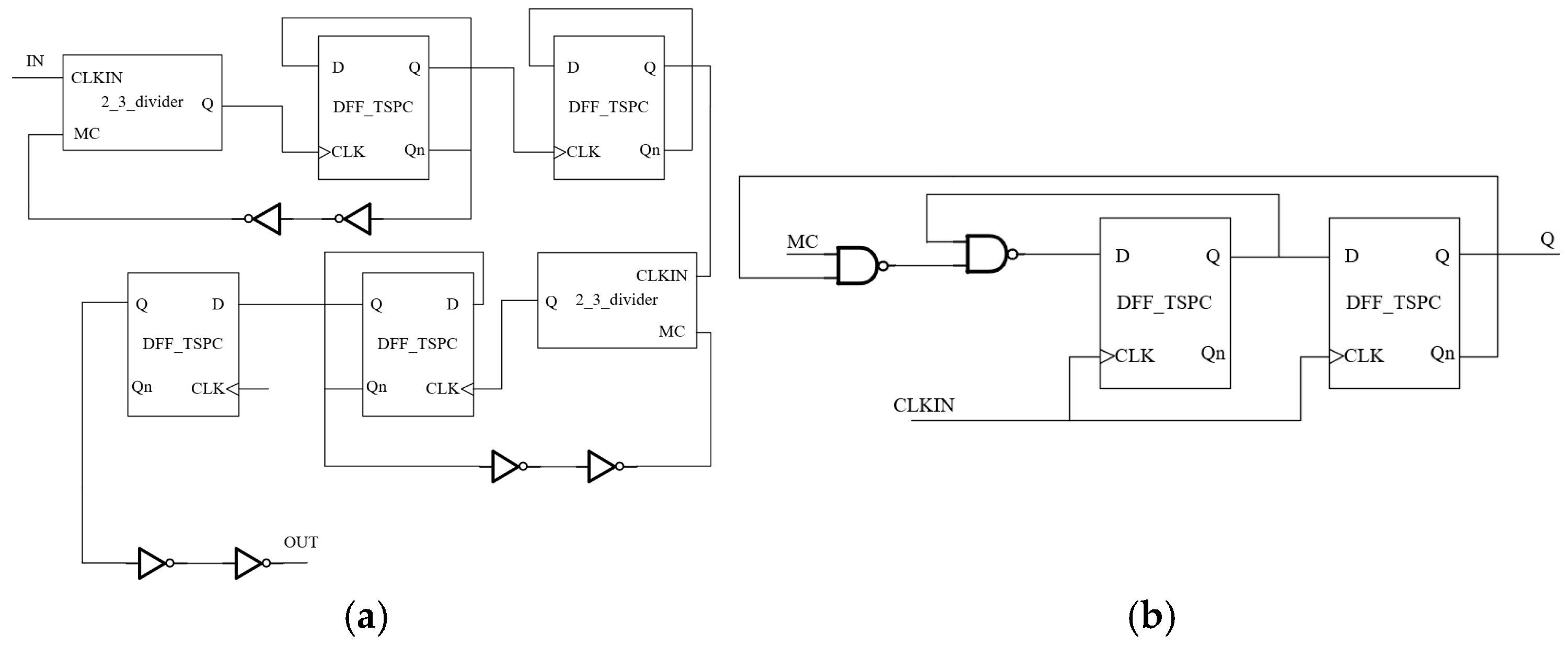
The crossover designed in this paper adopts an integer divider based on the 2_3 divider, and the specific structure is shown in
Figure 12a.
Figure 13 shows the transient simulation results of the frequency divider, which shows that the input frequency of the frequency divider is 800 MHz and the output frequency is 8 MHz, and the design circuit realizes a 100:1 frequency divider.
3.1. Simulation Results of Charge Pump Phase-Locked Loop
Figure 14 illustrates the linearized model of the charge pump phase-locked loop. Based on the linear approximations of individual modules (phase-frequency detector, charge pump, loop filter, and voltage-controlled oscillator), the loop gain transfer function
H(
s) of the PLL system can be derived as follows:
The phase-locked loop employs a second-order low-pass loop filter, thereby implementing a third-order charge pump phase-locked loop (CPPLL) architecture. This configuration enables the following:
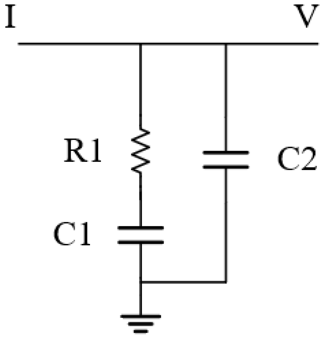
The resistor and capacitor values of the low-pass filter can be determined using the derived pole-zero locations and the maximum phase margin criterion. This method systematically optimizes the filter components to achieve target stability specifications while maintaining the desired closed-loop dynamics in the phase-locked loop system.
Figure 15 shows the 2nd order low-pass filter.
Among them, , , and are the zero point, the pole point, and the oop bandwidth separately.
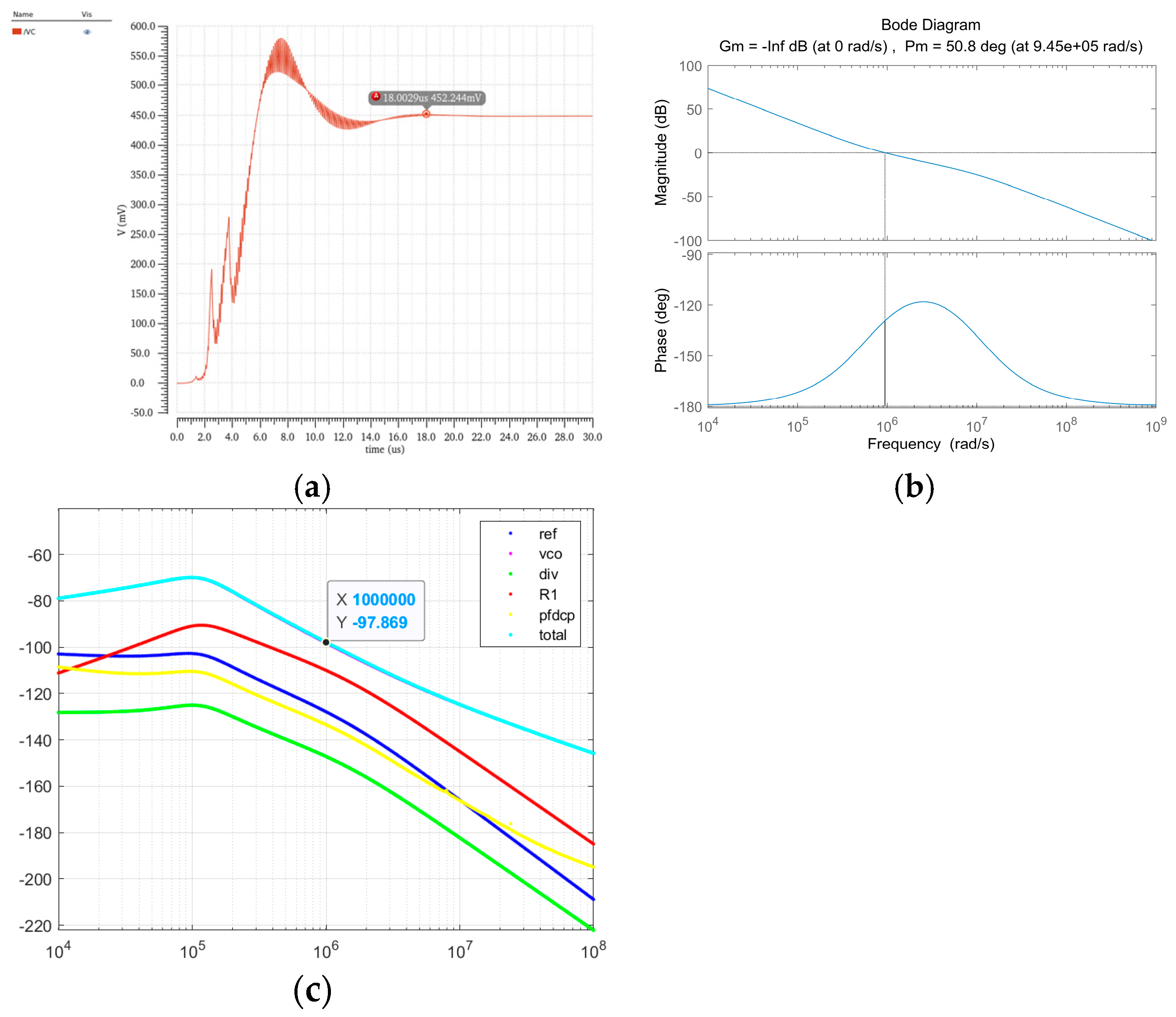
A transient simulation analysis was conducted on the complete charge pump phase-locked loop circuit.
Figure 16 presents the simulated locking process, demonstrating that the VCO control voltage Vctrl stabilizes at approximately 16 μs, with the CPPLL achieving phase lock after 18 μs. The system was modeled in MATLAB 2024 with the following parameters: reference frequency Fref = 8 MHz, charge pump current ICP = 20 μA, VCO gain KVCO = 400 MHz/V, and frequency division ratio N = 100. The simulated Bode plot in
Figure 16 reveals a loop bandwidth of 9.45 × 10
5 rad/s with a phase margin of 50.8, meeting stability requirements.
For precise phase noise characterization, systematic simulations were performed to evaluate noise contributions from individual components. Noise profiles of the phase-frequency detector, charge pump, loop filter, and VCO were extracted to construct a comprehensive noise transfer model. Using MATLAB’s phase noise fitting toolkit, the synthesized phase noise spectrum was obtained as shown in
Figure 16. The CPPLL exhibits an equivalent output phase noise of −98 dBc/Hz at 1 MHz offset, with detailed noise contributions from each subsystem clearly delineated across the frequency range. This hierarchical analysis methodology enables targeted optimization of dominant noise sources while maintaining loop stability constraints.
3.2. Principle of Charge Pump Phase-Locked Loop Circuit for Frequency Conditioning of MEMS Oscillators
The operational principle of this architecture converts the algorithmically derived frequency compensation quantity into a voltage signal through a frequency-to-voltage converter (FVC). This voltage is then summed with the output of the charge pump phase-locked loop low-pass filter via an analog summation circuit. The resulting composite voltage Vctrl dynamically controls the voltage-controlled oscillator, thereby generating a frequency output signal with precise compensation. This closed-loop configuration ensures continuous frequency stabilization by adaptively adjusting the VCO control voltage through the superimposed compensation component. The frequency-to-voltage conversion circuit architecture is illustrated in
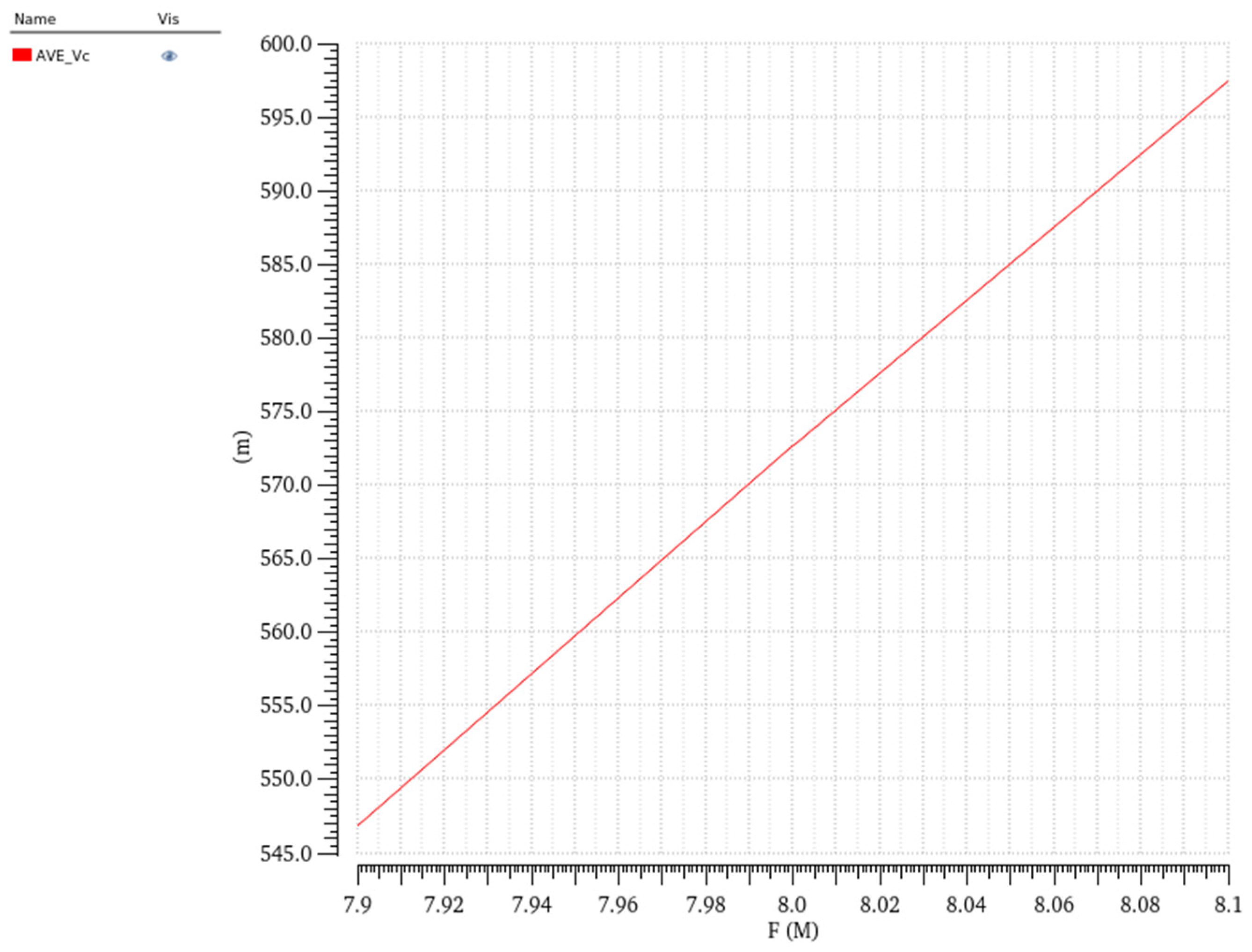
Figure 17b. This design employs an inverse phase-locked loop configuration to implement frequency–voltage conversion. By utilizing the tuning voltage of the voltage-controlled oscillator as the system output, a direct mapping relationship between input frequency and output voltage level is established. A phase-frequency detector monitors the phase difference between the input signal and the VCO feedback signal, generating output pulses whose width is proportional to frequency error, thereby achieving a quantitative measurement of the frequency deviation. These digital pulses from the PFD are subsequently converted into analog voltage signals through a low-pass filter, which attenuates high-frequency components to produce a smoothed tuning voltage. The system employs a closed-loop feedback mechanism to automatically adjust the VCO tuning voltage for frequency error cancellation. When input frequency variations occur, the loop dynamically regulates the output voltage level, ultimately establishing a linear correspondence between input frequency and output voltage at steady-state operation. The simulation results of the FVC are presented in
Figure 18. As demonstrated by these results, the circuit architecture exhibits a strong linear relationship between the output voltage and input frequency. This characteristic enables effective conversion of the frequency compensation quantity into corresponding control voltage increments, thereby precisely regulating the final output frequency through closed-loop adjustment. The linear transfer function validates the circuit’s capability to maintain proportional frequency correction across the operational bandwidth.
The effect of temperature changes on the output frequency is shown as follows.
Figure 19 shows the Frequency and temperature sweep simulation result of the CPPLL.
Table 2 shows the output frequency results at different temperatures.
Let
fMEMS denote the output frequency of the MEMS resonator,
fCPPLL represent the output frequency of the charge pump phase-locked loop, and
T indicate temperature. Under ideal conditions, where the MEMS resonator’s output frequency serves as the CPPLL’s input reference frequency, the relationship between these frequencies is governed by the following:
In this phase-locked loop configuration with
N = 100, taking 25 °C as the reference temperature, the input reference frequency to the charge pump PLL becomes the temperature-dependent MEMS resonant frequency
fMEMS(
T0) at temperature
T0. The temperature–frequency relationship of the MEMS resonator–PLL system was modeled through MATLAB curve fitting, yielding the following empirical expression:
The required frequency compensation relative to the reference frequency at 25 °C is given by the following:
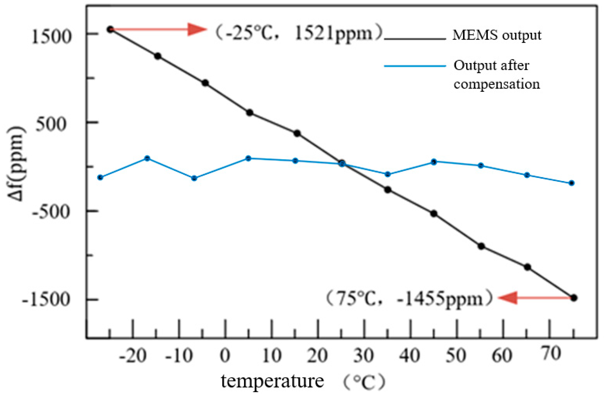
Temperature compensation simulations were conducted across the thermal range of −25 °C to +75 °C using 10 °C increments as test points. At each temperature, the algorithmically determined frequency compensation quantity was applied through the aforementioned circuit architecture. The compensated system output frequencies are tabulated in
Table 3, while the corresponding post-compensation frequency deviation characteristics are plotted in
Figure 20.
The graphical data demonstrate significant improvement in frequency–temperature stability after implementing the algorithmically derived frequency compensation calibration. Compared to the uncompensated MEMS resonator’s frequency drift, the compensated system reduces output frequency deviation to an average of 76 ppm across the operational temperature range of −25 °C to +75 °C.


