Abstract
This work details the design and experimental characterization of a 2D rectenna for scavenging radio frequency energy at 2.45 GHz (WiFi band), fabricated on polylactic acid polymer (PLA) using a plastronics approach. PLA is the RF substrate of both antenna and rectifier. The two transmission line (TTL) approach is used to characterize the substrate properties to be considered during design. A linearly polarized patch antenna with microstrip transmission feeding is connected to a single series diode rectifier through a T-matching network. The antenna has simulated and measured gain of 7.6 dB and 7.5 dB, respectively. The rectifier has a measured DC output power of 0.96 W at an optimal load of 2 k under RF input power of −20 dBm at 2.45 GHz. The power conversion efficiency is 9.6% in the latter conditions for a 54 × 36 mm patch antenna of a 1.5 mm thick PLA substrate obtained from additive manufacturing. The power conversion efficiency reaches a value of 28.75% when the input power is −10 dBm at 2.45 GHz. This corresponds to a peak DC power of 28.75 W when the optimal load is 1.5 k. The results compare significantly with the ones of a similar rectenna circuit manufactured on preferred RF substrate.
1. Introduction
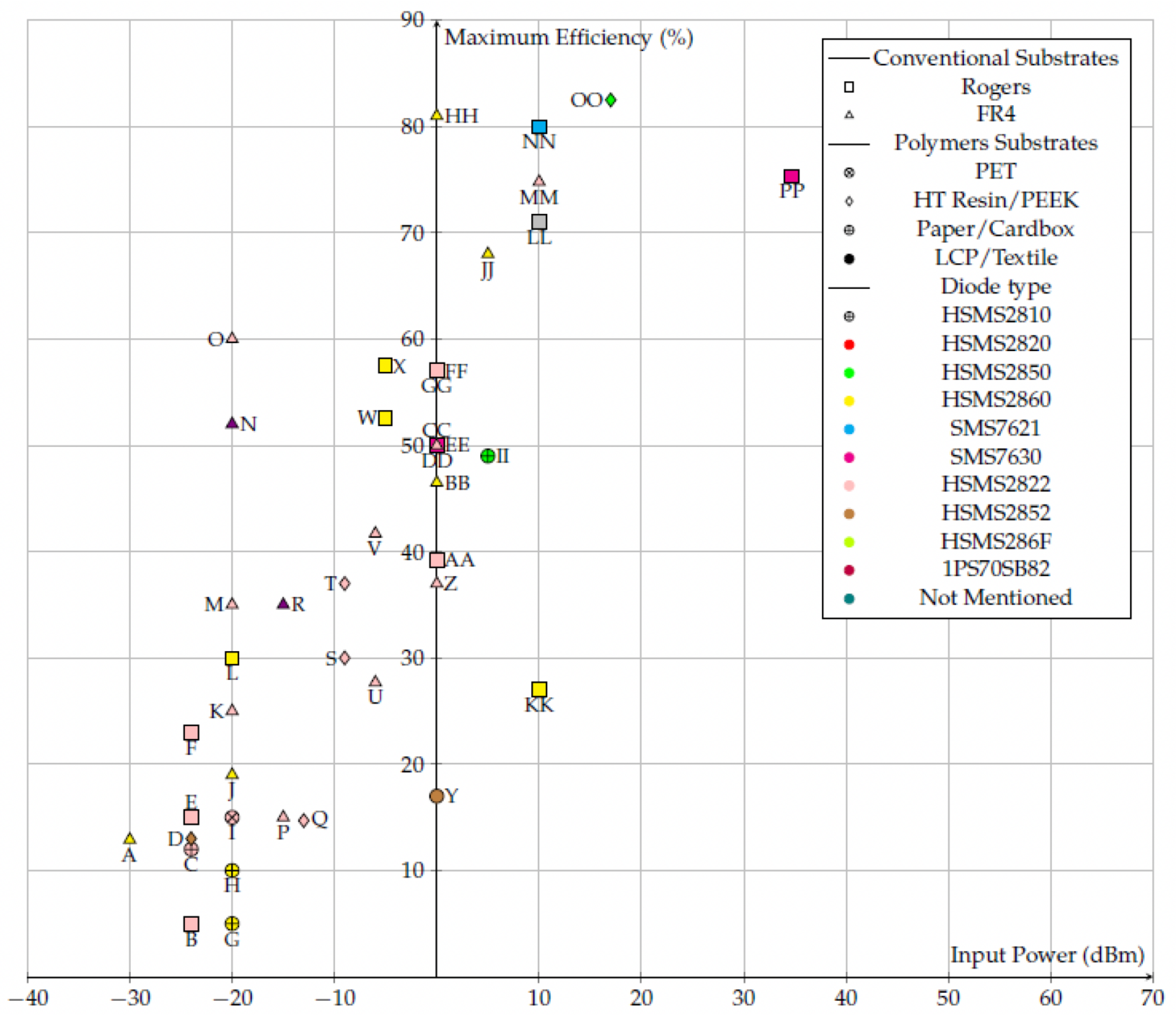
In 2018 and 2023, approximately 23.14 billion and 51.11 billion Internet of things (IoT) devices were, respectively, in operation. By 2030, close to 500 billion IOT devices will be connected [1]. Powering these devices is a challenge, especially in hard-to-reach areas at a time when batteries should be banned [2]. If nothing is done to improve the life span of batteries, close to 78 million will be dispatched daily by 2025 [3]. Natural energies available in the environment are in the forms of wind, thermal, mechanical vibrations, solar, friction, RF waves or organic wastes. Among them, radio frequency energy harvesting circuits become good candidates when there is no sun, wind or heat, or when objects are motionless. The major drawbacks of radio frequency energy harvesting are the low power density in the environment and the rapid fluctuation of the power level. Radio frequency energy harvesting (RFEH) circuits are often fabricated on non-recyclable substrates. Furthermore, most of these substrates cannot be used to create complicated 3D structures. To overcome these challenges, 3D additive manufacturing is becoming more and more popular but it is restricted to resin and polymer, for which RF properties are not considered in the first step. Polylactic acid polymer is presented as a bio-sourced material with great potential properties for recycling. Figure 1 summarises the recent state of the art on radio frequency energy harvesting circuits. The maximum power conversion efficiency (PCE) is plotted as a function of the RF input power. Most results consider an arbitrary DC load at the output of the rectifier; hence, it is not possible to evaluate if the maximum PCE is obtained under maximum power point conditions. The major focus is on the type of substrate. The majority of rectennas from the literature are constructed using conventional substrates (FR4 and Rogers). The graph in Figure 1 hides the size of the rectennas at hand. Generally, the smaller the size, the lower the PCE as the antenna gain decreases. Acceptable PCE values are nonetheless reported at ultra low RF input power (<−20 dBm). A received power of −20 dBm in WiFi band means in the best conditions that the rectenna (with an hypothetical gain of 10 dBi) is at 3 m maximum to the access point (Equivalent Isotropic Radiated Power (EIRP) of 20 dBm) or 8.7 m in RFiD @ 867 MHz (EIRP of 2 W). Low RF input power characterizes ambient RF energy scavenging as opposed to wireless power transfer where RF energy is voluntarily emitted in far-field conditions to the system to be powered. RF input power is then larger than -10 dBm in the latter application. Polyethylene tereftalate (PET) enables the fabrication of a rectenna with significant results [4] but PET is not recyclable. Indeed, few rectennas constructed on polymer substrates are reported. Paper or card box substrate rectennas have been reported as well [5] but 3D-shape objects may not be fabricated. PLA is not reported to the best of the authors’ knowledge.
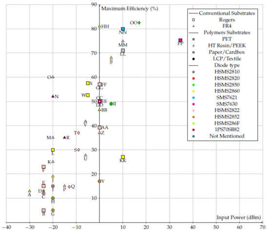
Figure 1.
Recent state of the art: Maximum Efficiency vs. Input Power depending on substrate type and diode reference. A-[6], B-[7], C-[5], D-[8], E-[7], F-[7], G-[9], H-[9], I-[4], J-[10], K-[11], L-[12], M-[11], N-[13], O-[11], P-[14], Q-[15], R-[13], S-[16], T-[16], U-[17], V-[17], W-[18], X-[18], Y-[19], Z-[20], AA-[21], BB-[22], CC-[22], DD-[23], EE-[24], FF-[25], GG-[21], HH-[26], II-[27], JJ-[10], KK-[28], LL-[29], MM-[20], NN-[30], OO-[11], PP-[31].
The fused deposition modelling (FDM) approach is selected for additive printing of PLA over stereolithography and laser sintering technologies. FDM is a cheap and easy 3D printing technology. The major disadvantages of FDM are the surface roughness of the finished structures and difficulties in mounting surface-mounted devices (SMDs). Techniques in reducing the surface roughness and brazing SMDs are reported in the work. The rest of this paper is organized as follows. In Section 2, the TTL method is used in extracting the RF properties of the polymer. The extracted results for loss tangent and relative permittivity is concerned. Section 3 details the fabrication and measurement result of the rectenna. Section 4 covers conclusions and perspectives.
2. Substrate Characterization
The substrate plays a key role in RF systems such as radio frequency energy harvesting circuits. The RF properties of the substrate are fundamental in designing the RF system. In this section, the two transmission line (TTL) method is deployed for extracting the loss tangent. The method allows to extract conductive losses and relative permittivity of the substrate. The TTL method is a simple method to be deployed over a wide band of frequencies. The TTL method was used in [8,32,33]. The principle of TTL is to calculate the phase, and the attenuation coefficient, introduced by different lines from the measured S-parameters. The attenuation coefficient is the real part in the propagation constant and it accounts for all the losses in the transmission line when the electromagnetic wave propagates through it. The phase constant is the imaginary part of the propagation constant. It determines the sinusoidal amplitude/phase of the signal along the transmission line at a constant time. Conductive losses (), dielectric loss tangent (tan) and relative permittivity () are determined from and .
The propagation constant is given by Equation (1) where is the attenuation coefficient of the transmission line (Np/m), is the phase constant of the transmission line (rad/m), is the angular velocity ().
The conductive loss of lines is given by Equation (2)
where R is the linear resistance (/m), is the conductivity of the conductor (S/m) and w is the width of the line.
consists of three loss contributions, namely, the dielectric loss (), conductive loss () and radiation loss (). The radiation loss () of the microstrip line is difficult to determine. In addition, the radiation loss is usually neglected compared to conductive and dielectric losses. In that perspective, Equation (1) is rewritten as:
2.1. Deployment of TTL
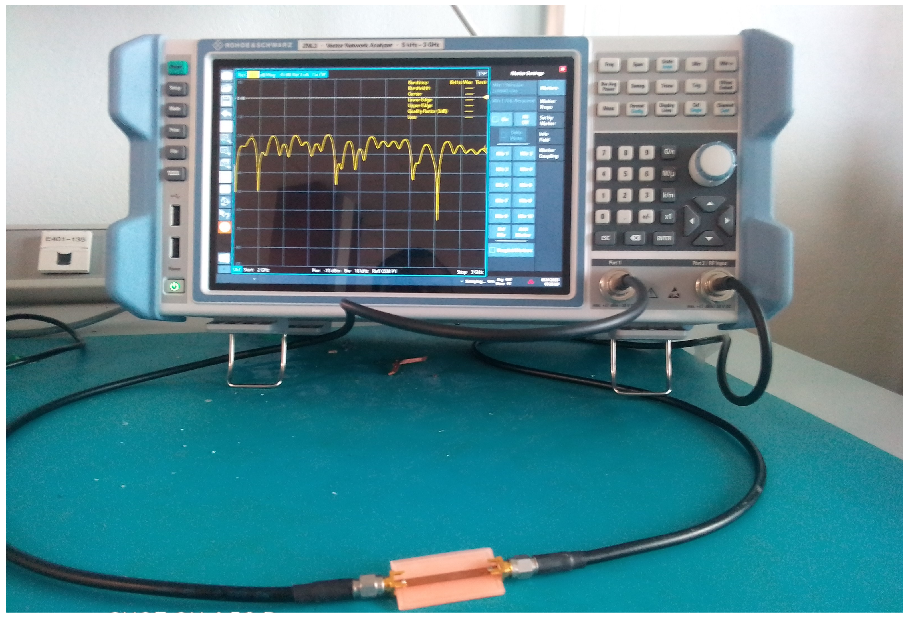
This method is deployed by fabricating at least two lines of the same width with different lengths. Lengths of 40 mm and 70 mm and width of 4.1 mm are selected on a 1.5 mm PLA substrate. Afterwards, the substrate thickness should not be changed.The configuration of the FDM printer is unchanged throughout the study. This is to ensure the best accuracy of the results when the substrate is used in designing RF circuits using the extracted losses tangent and relative permittivity parameters. The evaluation is to be repeated for any thickness of the substrate if this is to be a design parameter in the system. For the sake of simplicity, the work only evaluates one value of substrate thickness. PLA material is quite fragile so 1.5mm is the minimum thickness considered in this work. In any case, the thickness should not be too small as it affects the gain of the patch antenna. To ensure the accuracy of the result, two other pairs of lines of lengths (20 mm, 40 mm) and (50 mm, 70 mm) are fabricated and studied (Figure 2). The conductive material is a 35 m thick copper tape. The copper tape is easy to cut in any 2D shape with an acceptable accuracy. The laboratory setup for measuring the S-parameters of the lines is shown in Figure 3.
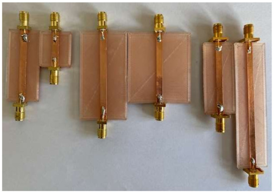
Figure 2.
Three-dimensional FDM-printed substrate transmission lines with copper tape.

Figure 3.
Deployment of the TTL for measuring the S-parameters. The measurement of S and S parameters shows good values below −38 dB.
2.2. Measurement Results
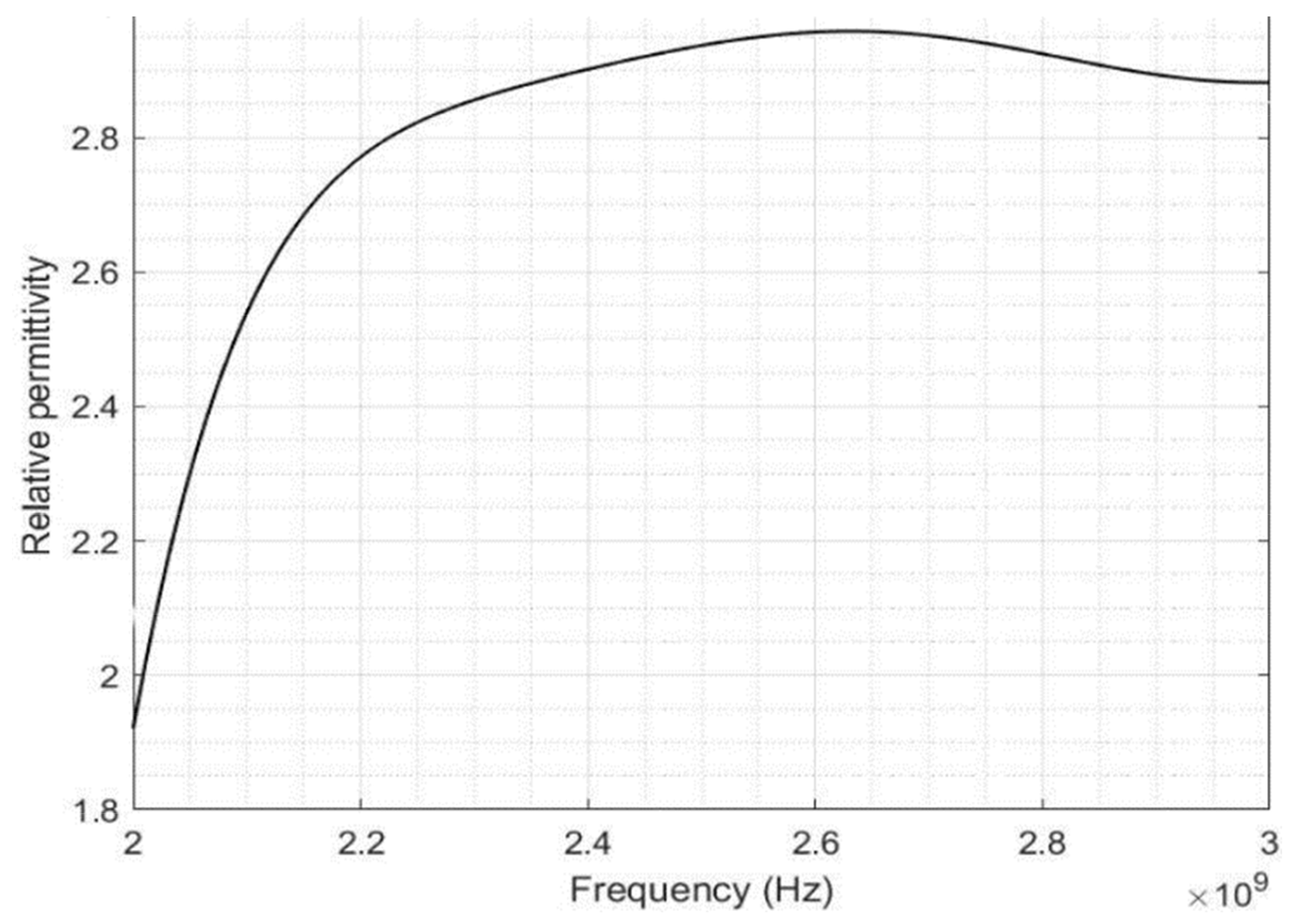
The R&S ZNL3 Vector Network Analyzer (VNA) is calibrated using the Short, Open, Load and Through (SOLT) calibration technique. The four S-parameters are measured and a script is written to determine the loss tangent and relative permittivity of the substrate. A third polynomial fitting function is used to interpolate the results. The measurement results for the relative permittivity and loss tangent are shown in Figure 4 and Figure 5, respectively. Similar results were obtained using the other pairs of lines.

Figure 4.
Measured Relative permittivity of PLA substrate in Figure 2.
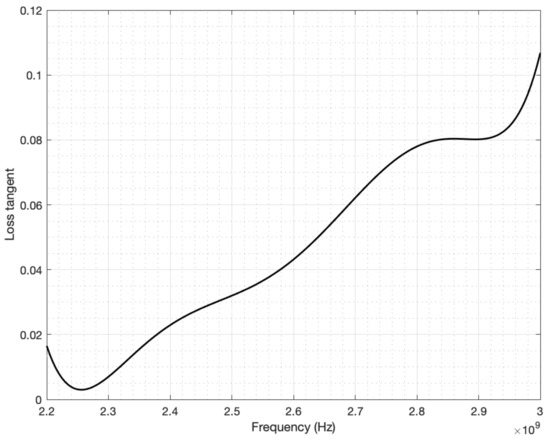
Figure 5.
Measured Loss tangent of PLA substrate in Figure 2.
The dispersion of results is related to the relative non-homogeneity of the printed PLA over a significant surface. Moreover, PLA is a porous material subject to water contamination. For more accurate results, the PLA samples should be kept in a conditioned-environment area prior to measurement. It was decided to account for the fact and let the PLA substrate be affected by the environment in order to anticipate the substrate change in RF properties at design level. The value of the relative permittivity at 2.45 GHz is 2.9 and the loss tangent is 0.01 in average. The variation of the results over the band of frequency can be due to roughness on the substrate and slight melting during brazing as well. The roughness and the melting change the RF properties of the PLA slightly. The results stabilize between 2.2 and 3 GHz with minor fluctuations. The mechanical properties of PLA are modest compared to those of resin. This accounts for the low melting temperature of PLA. However, the results are acceptable when compared with those in the state of the art (Table 1) to consider designing a radio frequency energy harvesting circuit.

Table 1.
Dielectric permittivity and loss tangent evaluated for PLA substrate in Figure 2 and compared to results from the state of the art.
3. Rectenna
Scavenging ambient RF energy requires a processing circuit. The simplest circuit should comprise an antenna or an array of antennas and a rectifying circuit. The rectifying circuit is usually constructed with one or more Schottky diodes. In this section, 2D shape circuits will be studied. We also evaluate the optimal load for the rectifier to obtain the maximum output power.
3.1. Antenna Design
A patch antenna is selected in this work due to its simplicity and easy fabrication process. The rectangular patch is designed at 2.45 GHz. The design equations for the length, Land width, W of the antenna are Equations (4) and (5), respectively [34,35].
where , , and are the wavelength, dielectric constant of the substrate and operating frequency, respectively. L and are the length extension and the effective dielectric constant of the antenna due to fringing effect. h is the thickness of the substrate. The antenna is simulated using CST Microwave software with the measured tan and . A micro-strip feedline is used to create the matching to 50 input impedance (Figure 6). The radiation parameters of the antennas are summarized in Table 2.
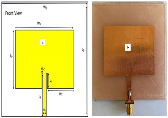
Figure 6.
Patch antenna printed on PLA and using copper tape as conductive material. (a) Geometry (with parameters in Table 2), (b) Fabricated patch.

Table 2.
Dimensions related to the antenna geometry (in mm) in Figure 6.
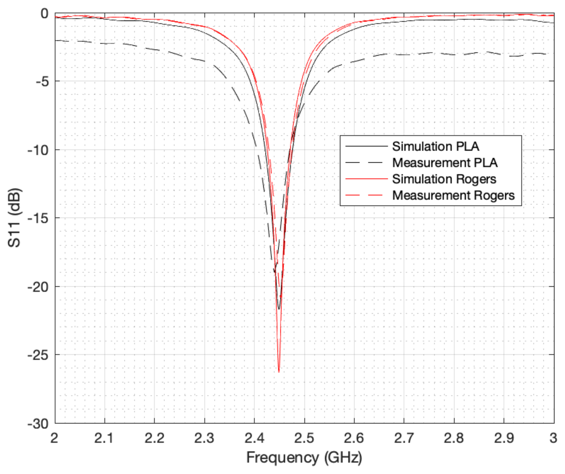
To ensure that the matching network is well designed and that the antenna can radiate, the return loss and gain of the antenna are measured. Both measurements give acceptable values. A similar antenna is designed on a standard RF substrate (Rogers 4003C) to study the effects of the relative permittivity and the loss tangent of PLA on the radiation properties of the antenna. The simulation and measurement of return losses of both antennas are shown in (Figure 7).
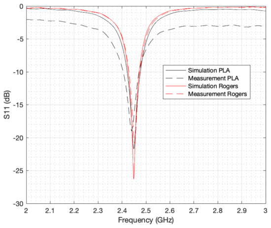
Figure 7.
Comparison of simulated and measured S of the patch antenna manufacturer on standard Rogers’ substrate and PLA, respectively.
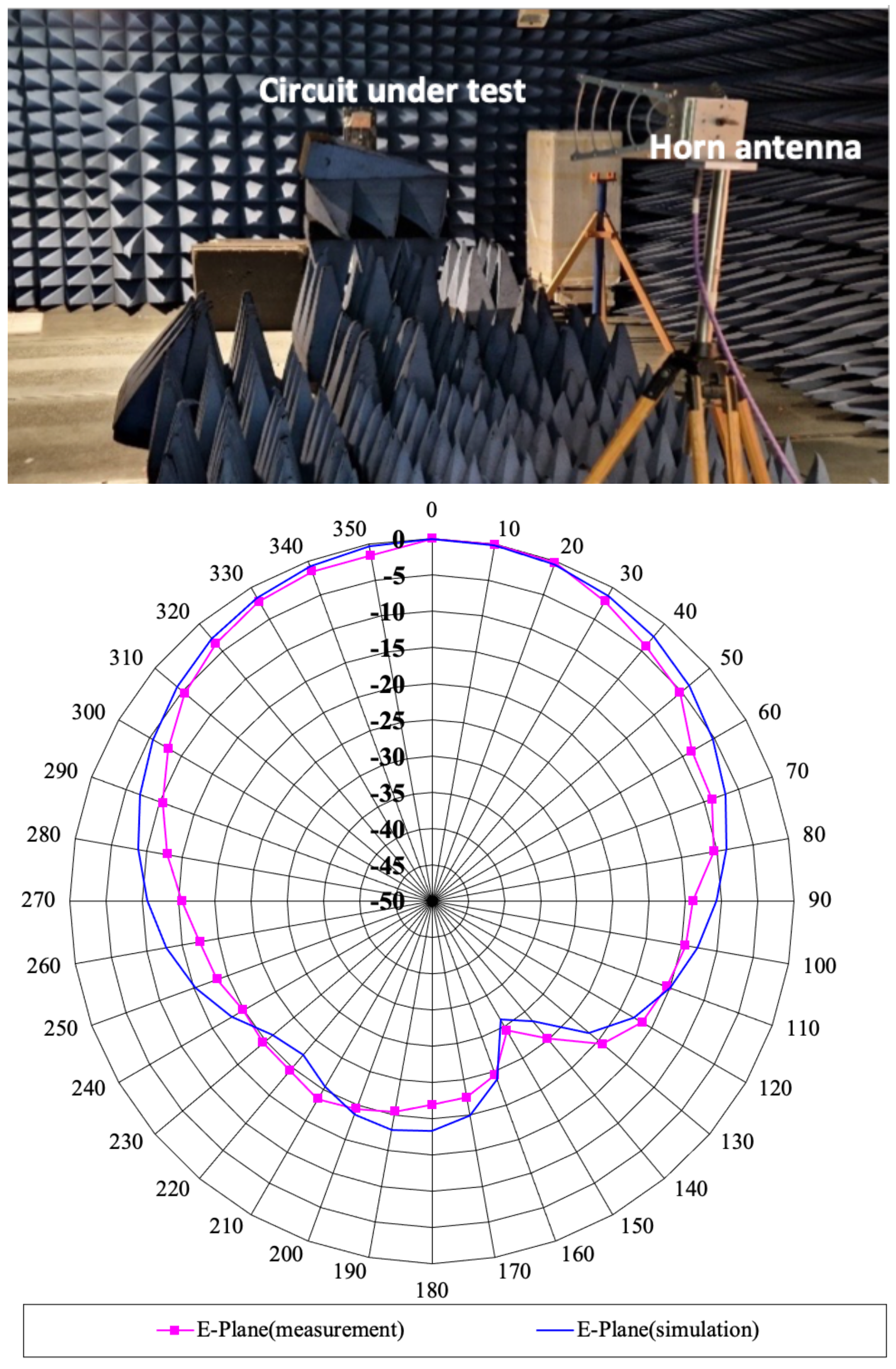
As seen in Table 3, both antennas have good return losses, with better results obtained for Rogers 4003C substrate. The rougher surface of PLA introduced more losses as compared to Rogers’ substrate. From the close match between simulation and measurement, it can be concluded that the average extracted values for tan and are acceptable to represent the RF behavior of PLA. The bandwidth of the antenna on PLA is higher than the one on Rogers’ substrate. This is because the relative permittivity of PLA is lower than that of Rogers’ substrate. In reference [36] it is shown that the bandwidth decreases with an increase in effective relative permittivity of the substrate. The shift in resonance frequency in measurement on PLA can be due to the variation in loss tangent and relative permittivity of PLA (Figure 4 and Figure 5). Again, the lower gain noticed in measurement of the patch antenna on PLA is due to substrate losses. The simulated and measured E-plane radiation pattern of the antenna in an anechoic chamber using a reference horn antenna of gain 9.8 dB at 2.45 GHz is shown in Figure 8 and summarized in (Table 3). The antenna has a linear polarisation parallel to the feedline.

Table 3.
Main properties of the patch antenna in (Figure 6).

Figure 8.
E−plane radiation pattern. (top) anechoic chamber (bottom) simulated and measured results.
3.2. Rectifier
RF signals from the antenna are converted to DC power with the help of a rectifying circuit. The single series diode (Half Wave Rectifier) topology in Figure 9 is selected due to its simplicity and better behavior in the case of low RF input power (ambient energy harvesting). Only a half cycle of the input wave is being rectified. The diode HSMS 2850 from Keysight offers a significant reverse breakdown voltage and low turn-on voltage. The diode model is available in Agilent ADS software including packaging parasitics (vendor model). The RF input power is set at −20 dBm as a specification. The rectifier is designed at 2.45 GHz. This frequency band is largely considered in the literature. Furthermore, it is not attenuated strongly in free space even under some weather conditions [37]. In this section, the fabrication and characterisation of the rectifier is concerned. The rectifier is validated by Momentum co-simulation in ADS 2022. Large signal scattering parameter (LSSP), harmonic balance simulation (HBS) and multiple parameters sweeps were used in simulation. HBS analysis is considered for optimizing the design with respect to DC output voltage, i.e., tuning an output filtering action. HBS is a frequency domain analysis technique for simulating distortion in non-linear circuits and systems. LSSP is performed on non-linear circuits and thus it takes into consideration non-linear effects such as gain compression and variation in power levels.

Figure 9.
Main rectifier schematic.
Matching Network Design
A T-matching network is constructed with microstrip lines. Microstrip lines offer fewer losses as compared to lumped elements though with more cumbersome circuits. The input matching network is based on a short circuit stub, which requires a via. The circuit has many via holes to the substrate. The electrical effect of these holes is mainly inductive and capacitive. Many formulas have been given in the literature to evaluate the values of the inductive and capacitive behavior of a via. The model of the via in [38] is adopted. The short-circuit stub behaves as an inductor of value L, since the calculated reactive value is positive. The length of the short-circuit is calculated using Equation (9). The length is further optimized through simulation. The input impedance of a lossless short-circuit stub is given by Equation (8)
where and Z are the guided wavelength and characteristics impedance, respectively.
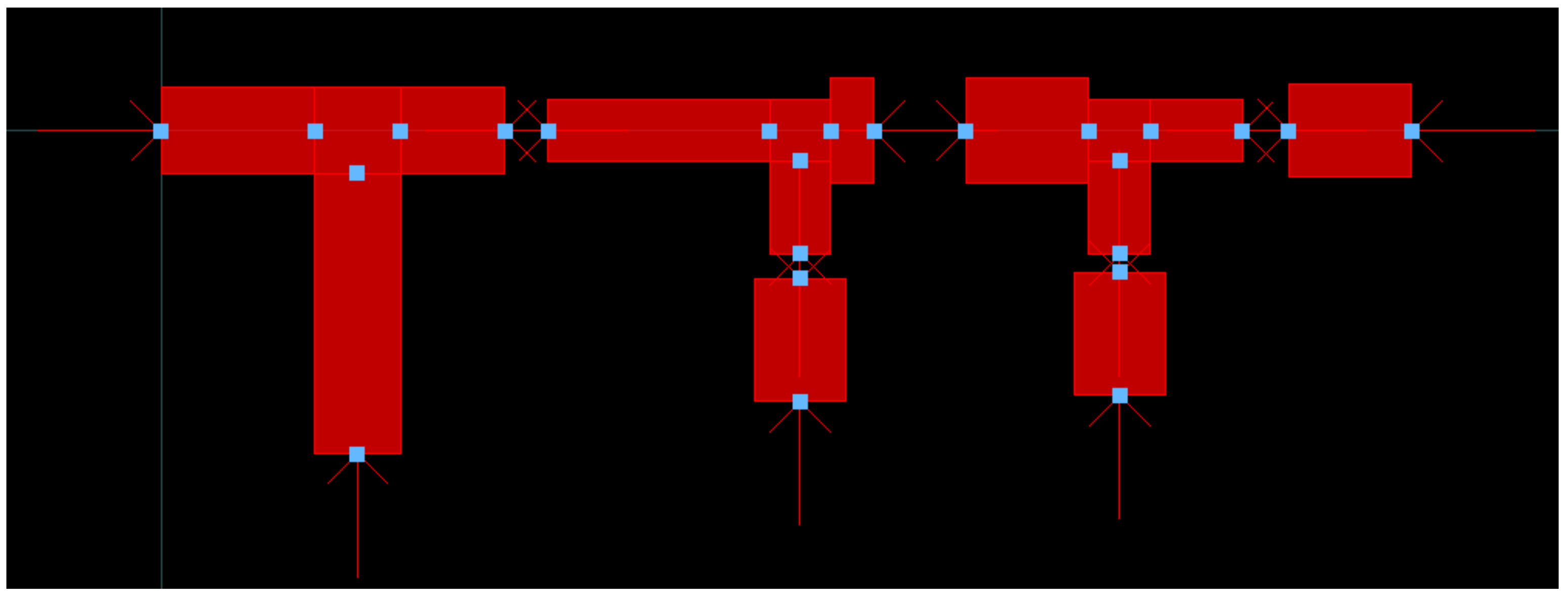
The geometry and fabricated circuit on 1.5 mm PLA are shown in (Figure 10).
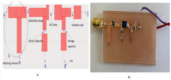
Figure 10.
Simulation and fabrication of rectifier (a) Momentum setup (b) Demonstrator.
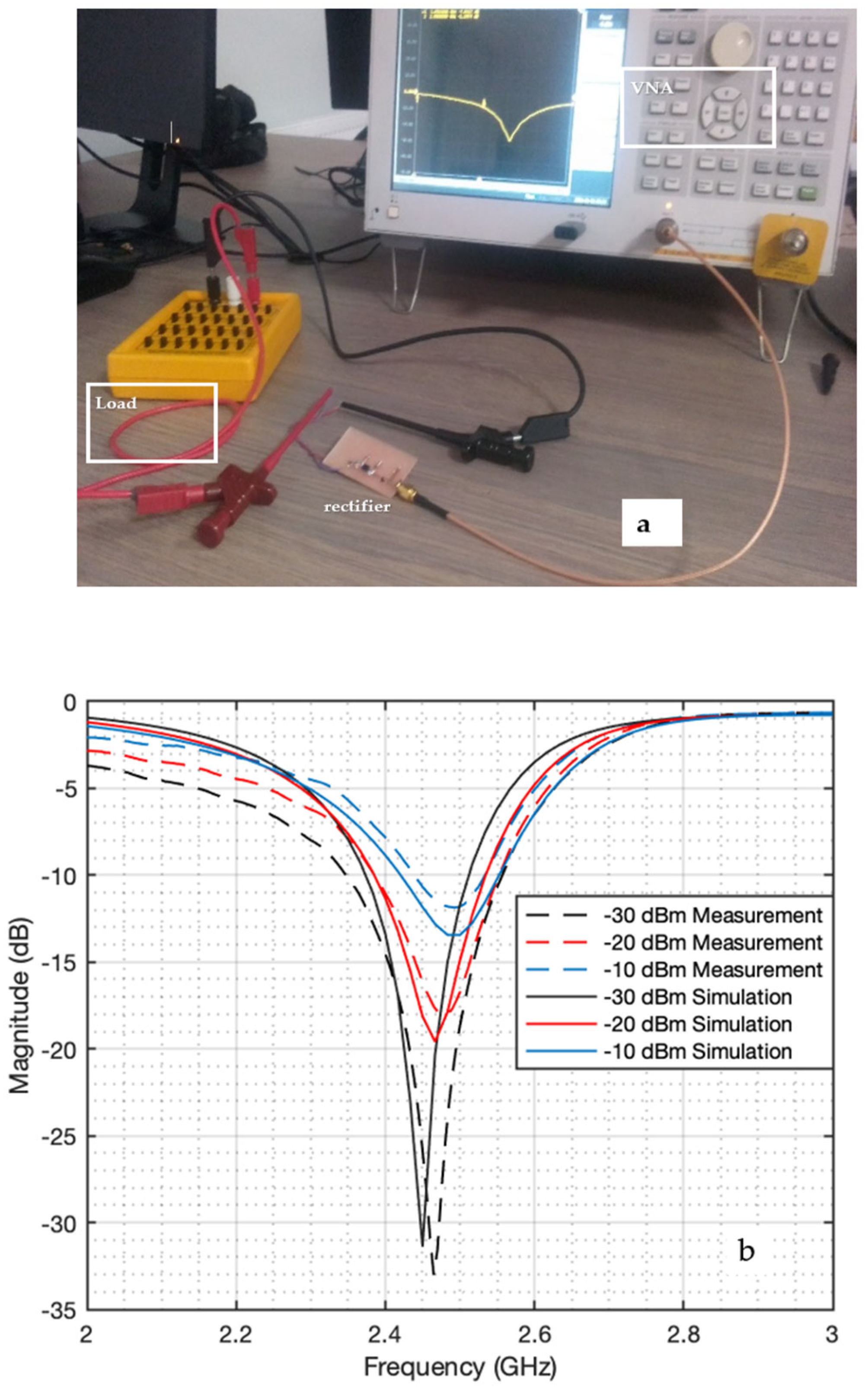
An RF choke is used to prevent harmonics from reaching the load. This is to increase the PCE. The laboratory setup, simulated and measured S of the rectifier at −30 dBm, −20 dBm and −10 dBm are, respectively, shown in (Figure 11). The measurement results have a shift in resonance frequency but with a good match at 2.45 GHz though lower than simulation value. The simulated and measured S at 2.45 GHz are −32 dB and −29 dB, respectively, at −30 Bm. This discrepancy might be due to the higher surface roughness of PLA and slight melting during brazing. It can also be caused by some inaccuracy in the diode packaging model.

Figure 11.
Measurement of return loss (a) lab-scale setup, (b) simulation and measurement of .
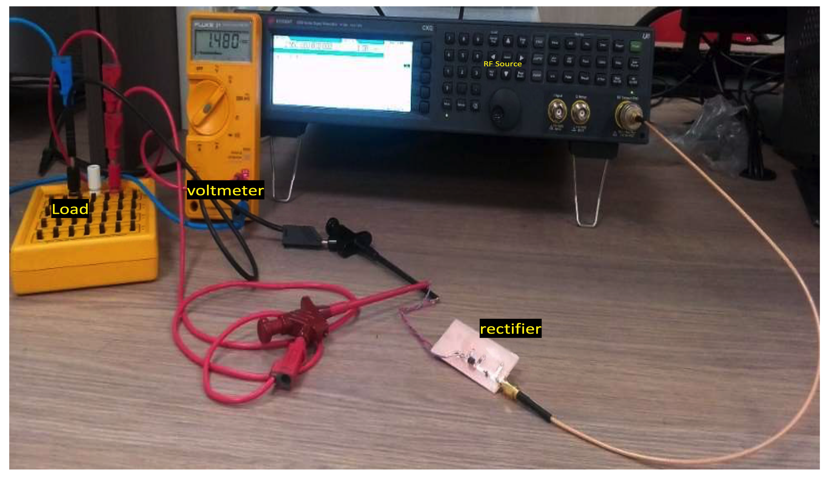
The laboratory setup for measuring the rectified DC voltage is shown in Figure 12. The DC power and PCE values are calculated using Equations (3) and (4), respectively.

Figure 12.
Lab-scale setup for measuring rectified voltage of PLA rectifier at 2.45 GHz while varying the load value.
3.3. Measurement and Maximum Power Point
In the setup in Figure 12, the rectified RF-DC power and PCE are calculated using Equations (10) and (11), respectively.
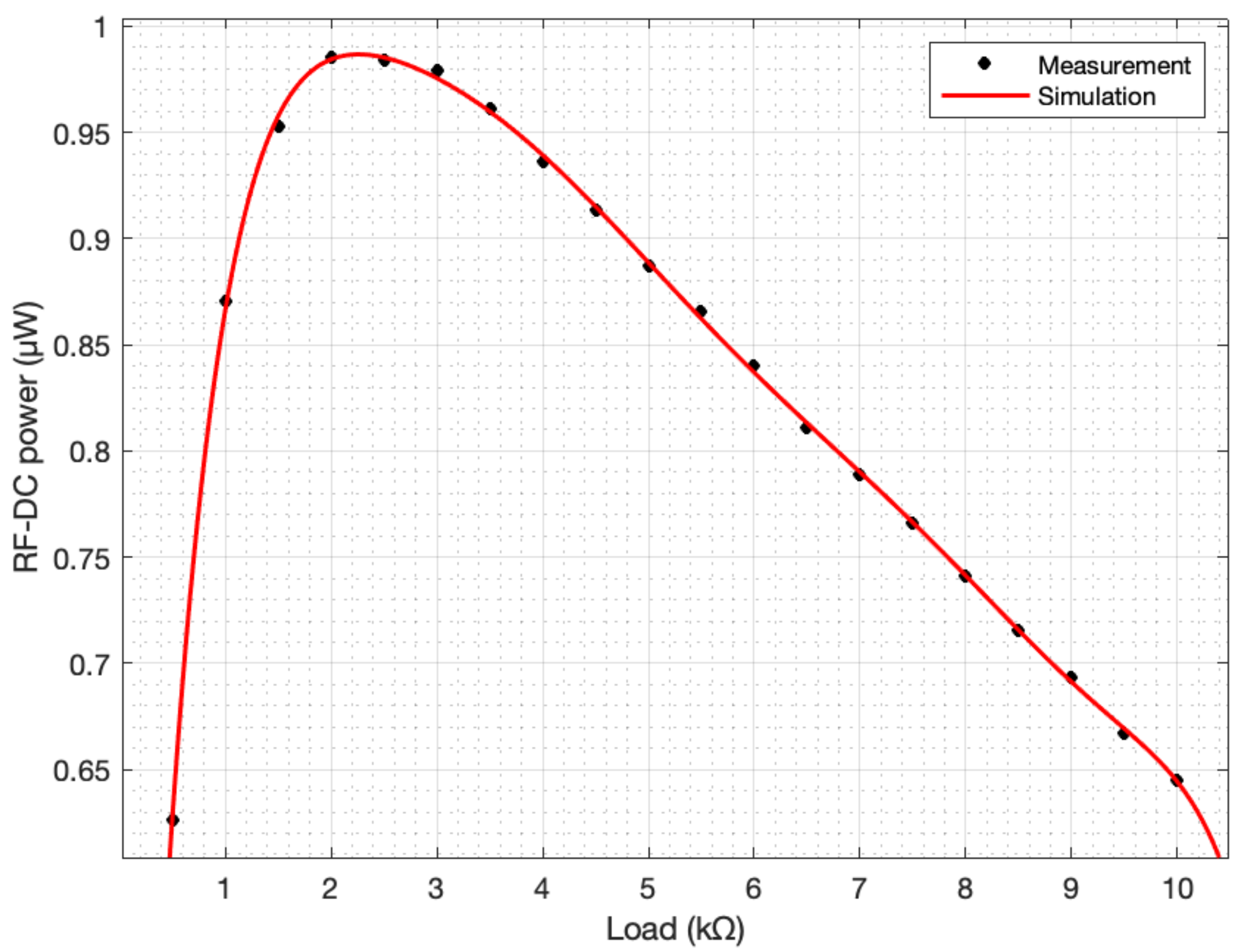
The simulated and measured results of DC output power under −20 dBm of input RF power are shown in Figure 12. The simulation setup was performed following the steps below.
- The simulation layout is generated from the schematic design software. Pins’ effects are added as lump components at the various gaps between ground and input power supply (Figure 13).
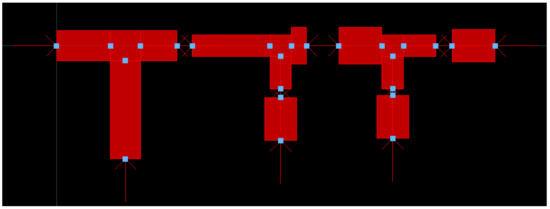 Figure 13. Layout setup for co-simulation.
 - The PLA substrate model is adjusted with the RF properties obtained from characterization in Section 2 (Figure 14).
 Figure 14. Setup and configuration of PLA substrate.
 - The frequency range is set between 2 GHz to 3 GHz in the momentum co-simulation.
- The lumped components, ground, power supply, via to ground and via to inductor are connected to the schematic in (Figure 10a).
As seen in Figure 15, the measurement has the same tendency as in the simulation with a very close match between the two. It should be noted that SMA and measuring cable losses were taken into consideration during simulation. This explains the close match between simulation and measurement.
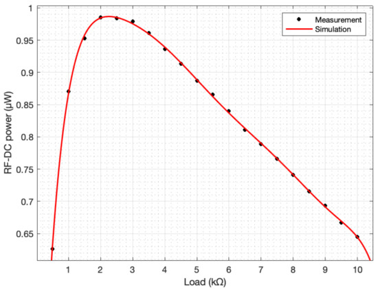
Figure 15.
Simulated and measured DC output power under −20 dBm input RF power at 2.45 GHz.
The maximum power point (MPP) condition is investigated through varying the DC load until identifying a maximum of output DC power. Figure 15 indicates a maximum available power of 0.98 W under −20 dBm input RF power at 2.45 GHz. The so-called optimal DC load is also determined (2.2 k in Figure 15). A simple model of the rectifier output may be an ideal voltage source (open-circuit DC voltage) in a series with a resistive impedance of the optimal load value. This is only representing the MPP condition.
The results of MPP conditions are presented in Figure 16 under input RF power of −25 dBm, −15 dBm and −10 dBm.
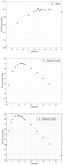
Figure 16.
Measured DC output power under RF input power conditions at 2.4 GHz of −25 dBm (top), −15 dBm (medium), −10 dBm (bottom).
The measured PCE of the PLA-based rectifier is compared with that of the rectifiers designed on standard substrates and other polymers from the state of the art (Table 4). The table shows that the fabricated PLA-based rectifier features acceptable results. It can also be concluded that the fabrication method has no significant impact on the performance of rectennas. Hence, compared to SLA resin 3D printing, i.e., the result in [8], 3D FDM printing offers acceptable results and represents a cost-effective solution for an RFEH circuit.
The DC open-circuit voltage at −10 dBm, −15 dBm and −20 dBm are 420 mV, 214.65 mV, and 43.46 mV, respectively. The literature covers the issue of cold startup of electronic systems supplied from energy harvesting circuits. An electrical energy conversion circuit is generally implemented between the harvesting circuit and the payload system to be supplied (like a sensor). The case of a radio frequency energy harvesting circuit is particular as the output impedance is large compared to the case of photovoltaic scavengers. This issue has been addressed in the literature and the state of the art situates the required minimal DC open-circuit voltage of the RFEH circuit between 180 mV and 200 mV. The PLA-based rectifier presented here would require an RF input power between −15 dBm and −17 dBm to support the cold-startup of the electronic system connected at its output.
In general, the DC power is usually low for RF energy harvesting systems as compared to other kinds of harvesters. This is due to the following.
- Parasitics: the existence of parasitic components in the diode may limit the PCE. The diode junction resistor, R, causes losses. At high frequency, the junction capacitance and package inductance also limit the PCE [39].
- Threshold and reverse-breakdown voltage: the diode threshold voltage requires the energy harvester to be supplied with sufficient input RF power. This limits the sensitivity of the RFEH circuit. The effect of diode breakdown voltage occurs when the diode DC bias voltage is half the breakdown voltage. This is why the power curves in Figure 15 and Figure 16 begin to decrease above this point.
- Harmonics at the output: the non-linearity of the diode creates harmonics in the output voltage, responsible for losses.
- Impedance matching: as the diode behavior changes with the input RF power, the input matching deviates and part of the incident energy is reflected to the surroundings. This reflected power causes a reduction in the amount of energy available for rectification. PCE is negatively impacted.
4. Conclusions
This work addresses the fabrication of antenna and rectifier on a 2D polymer structure, namely, PLA, printed by FDM. This allows 3D shapes as well. The literature mentions results on printed antennas in 3D polymer structures [5,40,41,42,43,44,45,46], but to the best of our knowledge, only one author [8] mentioned the fabrication of rectifier on polymer substrate using resin, and none on PLA. PLA as the chosen polymer for substrate has been primarily identified in terms of RF properties to support design of a rectenna. The TTL method has been applied and verified over different pairs of lines. RF properties are subject to variation but remain significant enough to envisage practicable radio frequency energy harvesting circuits with acceptable PCE. The antenna and the rectifier substrates are printed using FDM, also called fuse filament fabrication, for the sake of cost and simplicity. The drawbacks of FDM are the surface roughness of the parts after printing and the low melting temperature of the structure, making it difficult to braze SMDs on the surface. Using copper tape to create the conductive line of circuit layout is a pragmatic and cost-effective solution, enabling 3D shapes. A patch antenna reveals a gain in line with literature results based on other material. There is no gain in performance but the advantage is the use of a bio-sourced material, ready for recycling, which is not the case of numerous other materials. The obtained power conversion efficiency is in line with other literature results, somewhat lower but not much. At low RF input power, −25 dBm and 20 dBm, the maximum available DC power is, respectively, 0.14 W and 0.96 W at 2.45 GHz. Future work will consist in treating the PLA substrate surface to reduce losses. RF properties will be improved. A multi-polarised antenna will be considered to increase the beamwidth of the antenna. In conclusion, this work demonstrates the viability of a rectenna manufactured on PLA substrate using plastronics.

Table 4.
Comparison with the state of the art.
Table 4.
Comparison with the state of the art.
| Frequency (GHz) | Pin(dBm)@ Load (k) | PCE@RF-DC Power | Substrate/Printing Tech | Size (mm × mm × mm) | Ref |
|---|---|---|---|---|---|
| 2.45 | −24@10 | 13%@0.52 W | Resin/Stereolithography 3D printing polymer | 60 × 83 × 1.5 | [8] |
| 2.45 | −20@1 | 5%@0.5 W | LCP/Not mention | 15.1 × 8.15 × 0.18 | [25] |
| 2.45 | −20@1 | 5%@0.5 W | LCP/Not mention | 15.1 × 8.15 × 0.18 | [25] |
| 2.5 | −20@3 | 5%@0.5 W | Flexible paper/copper tape | 11 × 11 × 0.37 | [9] |
| 2.3 | −24@14.7 | 5%@0.2 W | Duroid 5880/Conventional deposition (Rectifier)(PCB) | 32 × 32 × 1.575 | [7] |
| 2.4 | −20@6.81 | 13%@1.3 W | FR4/printed circuit board | 32.07 × 35.75 × 1.6 | [13] |
| 0.915 | 0@6.8 | 55%@550 W | flexible printed circuit board (PCB) | Not Mentioned | [47] |
| 2.45 | −24.3@4 | 21%@0.78 W | Duroid 5880/ Conventional deposition (Rectifier)(PCB) | 105 × 87 × 3.7 | [48] |
| 2.45 | −20@14.7 | 15%@1.5 W | Duroid 5880/ Conventional deposition (Rectifier)(PCB) | 32 × 32 × 1.575 | [7] |
| 2.1 | −24@11 | 3%@0.12 W | 3D printing substrate/Screen printing (conductive silver paste from DuPont) | 50 × 50 × 50 | [5] |
| 2.45 | −15@1.7 | 19%@ 6 W | PLA/Fuse Deposition Modelling 3D printing polymer | 42 × 14 × 1.5 | This Work |
| −20@2 −25@3.9 −10@1.5 | 9.6%@0.96 W 4.43%@0.14 W 28.75%@ 28.75 |
Author Contributions
Methodology, J.V.; Validation, J.-M.D. and P.B. (Philippe Bnench); Investigation, P.U.L., T.G. and P.L.; Resources, P.B. (Pascal Bevilacqua); Data curation, F.M.; Writing—original draft, B.A.; Project administration, M.C. Funding acquisition, P.T. and B.A. All authors have read and agreed to the published version of the manuscript.
Funding
This research was funded by project IPCEI Nano 2022—INCA.
Acknowledgments
The authors wish to thank the support of Region Auvergne-Rhone-Alpes regarding 3D Plastronics within the COMSUP program.
Conflicts of Interest
The authors declare no conflict of interest.
Abbreviations
The following abbreviations are used in this manuscript:
| DC | Direct Current |
| RFEH | Radio Frequency Energy Harvesting |
| HBS | Harmonic Balance Simulation |
| LSSP | Large Signal Scattering Parameter |
| MPP | Maximum Power Point |
| PCE | Power Conversion Efficiency |
| PLA | Polylactic Acid polymer |
| TTL | Two Transmission Line |
References
- Newell, D. Optimised Energy Management for Energy Harvesting Powered Wireless Sensors; NUI Galway: Galway, Ireland, 2018. [Google Scholar]
- Sezer, N.; Koç, M. A comprehensive review on the state-of-the-art of piezoelectric energy harvesting. Nano Energy 2021, 80, 105567. [Google Scholar] [CrossRef]
- European Comission. Up to 78 Million Batteries Will Be Discarded Daily by 2025, Researchers Warn; European Comission: Brussels, Belgium, 2021.
- Georgiadis, A.; Collado, A.; Via, S.; Meneses, C. Flexible hybrid solar/EM energy harvester for autonomous sensors. In Proceedings of the MTT-S International Microwave Symposium Digest, Baltimore, MD, USA, 4–11 June 2011; pp. 6–9. [Google Scholar] [CrossRef]
- Bakytbekov, A.; Nguyen, T.Q.; Huynh, C.; Salama, K.N.; Shamim, A. Fully Printed 3D Cube-Shaped Multiband Fractal Rectenna for Ambient RF Energy Harvesting. Nano Energy 2018, 53, 587–595. [Google Scholar] [CrossRef]
- Muhammad, S.; Tiang, J.J.; Wong, S.K.; Smida, A.; Ghayoula, R.; Iqbal, A. A Dual-Band Ambient Energy Harvesting Rectenna Design for Wireless Power Communications. IEEE Access 2021, 9, 99944–99953. [Google Scholar] [CrossRef]
- Song, C.; Huang, Y.; Zhou, J.; Zhang, J.; Yuan, S.; Carter, P. A high-efficiency broadband rectenna for ambient wireless energy harvesting. IEEE Trans. Antennas Propag. 2015, 63, 3486–3495. [Google Scholar] [CrossRef]
- Linh Nguyen, X.V.; Gerges, T.; Duchamp, J.M.; Benech, P.; Verdier, J.; Lombard, P.; Cabrera, M.; Allard, B. Stereolithography-Based Rectenna for Wireless Energy Harvesting. In Proceedings of the 34th International System-on-Chip Conference (SOCC), Las Vegas, NV, USA, 14–17 September 2021; pp. 34–39. [Google Scholar] [CrossRef]
- Palazzi, V.; Hester, J.; Bito, J.; Alimenti, F.; Kalialakis, C.; Collado, A.; Mezzanotte, P.; Georgiadis, A.; Roselli, L.; Tentzeris, M.M. A Novel Ultra-Lightweight Multiband Rectenna on Paper for RF Energy Harvesting in the Next Generation LTE Bands. IEEE Trans. Microw. Theory Tech. 2018, 66, 366–379. [Google Scholar] [CrossRef]
- Awais, Q.; Jin, Y.; Chattha, H.T.; Jamil, M.; Qiang, H.; Khawaja, B.A. A Compact Rectenna System With High Conversion Efficiency for Wireless Energy Harvesting. IEEE Access 2018, 6, 35857–35866. [Google Scholar] [CrossRef]
- Roy, S.; Tiang, J.J.; Roslee, M.B.; Ahmed, M.T.; Kouzani, A.Z.; Mahmud, M.P. Quad-band rectenna for ambient radio frequency (RF) energy harvesting. Sensors 2021, 21, 7838. [Google Scholar] [CrossRef]
- Hucheng, S.; Guo, Y.-X.; He, M.; Zhong, Z. A dual-band rectenna using broadband yagi antenna array for ambient rf power harvesting. IEEE Antennas Wirel. Propag. Lett. 2013, 12, 918–921. [Google Scholar] [CrossRef]
- Roy, S.; Tiang, J.J.; Roslee, M.B.; Ahmed, M.T.; Kouzani, A.Z.; Mahmud, M.P. Design of a Highly Efficient Wideband Multi-Frequency Ambient RF Energy Harvester. Sensors 2022, 22, 424. [Google Scholar] [CrossRef]
- Hamidouche, A.M.; Takhedmit, H.; Poulichet, P.; Cirio, L. Efficiency improvement of an UWB rectifier by using optimized pulse modulation signal: Simulation and experiments. In Proceedings of the Wireless Power Week (WPW), Bordeaux, France, 5–8 July 2022; pp. 407–411. [Google Scholar] [CrossRef]
- Nguyen, X.V.L.; Gerges, T.; Duchamp, J.M.; Benech, P.; Verdier, J.; Lombard, P.; Cabrera, M.; Allard, B. 3D Plastronics Radio Frequency Energy Harvester on Stereolithography Parts. In Proceedings of the Wireless Power Week (WPW), Bordeaux, France, 5–8 July 2022; pp. 156–161. [Google Scholar] [CrossRef]
- Niotaki, K.; Kim, S.; Jeong, S.; Collado, A.; Georgiadis, A.; Tentzeris, M.M. A Compact Dual-Band Rectenna Using Slot-Loaded Dual Band Folded Dipole AntennaKyriaki. IEEE Antennas Wirel. Propag. Lett. 2013, 12, 1634–1637. [Google Scholar] [CrossRef]
- Khalid, F.; Saeed, W.; Shoaib, N.; Khan, M.U.; Cheema, H.M. Quad-Band 3D Rectenna Array for Ambient RF Energy Harvesting. Int. J. Antennas Propag. 2020, 2020, 7169846. [Google Scholar] [CrossRef]
- Shen, S.; Chiu, C.Y.; Murch, R.D. A dual-port triple-band L-probe microstrip patch rectenna for ambient RF energy harvesting. IEEE Antennas Wirel. Propag. Lett. 2017, 16, 3071–3074. [Google Scholar] [CrossRef]
- Lin, C.H.; Chiu, C.W.; Gong, J.Y. A Wearable Rectenna to Harvest Low-Power RF Energy for Wireless Healthcare Applications. In Proceedings of the 11th International Congress on Image and Signal Processing, BioMedical Engineering and Informatics (CISP-BMEI), Beijing, China, 13–15 October 2018; pp. 1–5. [Google Scholar] [CrossRef]
- Mansour, M.M.; Kanaya, H. Compact RF rectifier circuit for ambient energy harvesting. In Proceedings of the International Symposium on Radio-Frequency Integration Technology, RFIT 2017, Seoul, Republic of Korea, 30 August–1 September 2017; pp. 220–222. [Google Scholar] [CrossRef]
- Ur Rehman, M.; Ahmad, W.; Khan, W.T. Highly efficient dual band 2.45/5.85 GHz rectifier for RF energy harvesting applications in ISM band. In Proceedings of the Asia-Pacific Microwave Conference, Kuala Lumpur, Malaysia, 13–16 November 2017; pp. 150–153. [Google Scholar] [CrossRef]
- Tafekirt, H.; Pelegri-Sebastia, J.; Bouajaj, A.; Reda, B.M. A Sensitive Triple-Band Rectifier for Energy Harvesting Applications. IEEE Access 2020, 8, 73659–73664. [Google Scholar] [CrossRef]
- Almoneef, T.S. Design of a Rectenna Array without a Matching Network. IEEE Access 2020, 8, 109071–109079. [Google Scholar] [CrossRef]
- Eid, A.; Costantine, J.; Tawk, Y.; Ramadan, A.H.; Abdallah, M.; Elhajj, R.; Awad, R.; Kasbah, I.B. An efficient RF energy harvesting system. In Proceedings of the 11th European Conference on Antennas and Propagation, EUCAP 2017, Paris, France, 19–24 March 2017; pp. 896–899. [Google Scholar] [CrossRef]
- Eid, A.; Hester, J.G.; Costantine, J.; Tawk, Y.; Ramadan, A.H.; Tentzeris, M.M. A Compact Source-Load Agnostic Flexible Rectenna Topology for IoT Devices. IEEE Trans. Antennas Propag. 2020, 68, 2621–2629. [Google Scholar] [CrossRef]
- Papadopoulou, M.S.; Boursianis, A.D.; Volos, C.K.; Stouboulos, I.N.; Nikolaidis, S.; Goudos, S.K. High-Efficiency Triple-Band RF-to-DC Rectifier Primary Design for RF Energy-Harvesting Systems. Telecom 2021, 2, 271–284. [Google Scholar] [CrossRef]
- Khonsari, Z.; Björninen, T.; Tentzeris, M.M.; Sydänheimo, L.; Ukkonen, L. 2.4 GHz inkjet-printed RF energy harvester on bulk cardboard substrate. In Proceedings of the Radio and Wireless Symposium (RWS), San Diego, CA, USA, 25–28 January 2015; pp. 153–155. [Google Scholar] [CrossRef]
- Mouapi, A.; Hakem, N.; Kandil, N.; Kamani, G.V. A Miniature Rectifier Design for Radio Frequency Energy Harvesting Applied at 2.45 GHz. In Proceedings of the International Conference on Environment and Electrical Engineering and Industrial and Commercial Power Systems Europe, EEEIC/I and CPS Europe 2018, Palermo, Italy, 12–15 June 2018; pp. 1–5. [Google Scholar] [CrossRef]
- Asakura, S.; Yamanokuchi, S.; Yoshida, S.; Nishikawa, K. Design and Prototyping of a Single-Shunt Rectifier with 71% Fractional Bandwidth Having Acceptable Matching on 10 dBm LSSP. In Proceedings of the Wireless Power Week (WPW), Bordeaux, France, 5–8 July 2022; pp. 383–387. [Google Scholar] [CrossRef]
- Hoque, M.U.; Kumar, D.; Audet, Y.; Savaria, Y. Design and Analysis of a 35 GHz Rectenna System for Wireless Power Transfer to an Unmanned Air Vehicle. Energies 2022, 15, 320. [Google Scholar] [CrossRef]
- Kawai, K.; Takabayashi, N.; Toyonaga, T.; Suzuki, K.; Shinohara, N. Development of Rectenna for Estimating Received Power Level Using Second Harmonic Wave. In Proceedings of the Wireless Power Week (WPW), Bordeaux, France, 5–8 July 2022; pp. 175–179. [Google Scholar] [CrossRef]
- Ferrari, P.; Flechet, B.; Angenieux, G. Time domain characterization of lossy arbitrary characteristic impedance transmission lines. IEEE Microw. Guid. Wave Lett. 1994, 4, 177–179. [Google Scholar] [CrossRef]
- Mpele, M.P.; Mbango, F.M.; Konditi, D.B.O.; Ndagijimana, F. A novel quadband ultra miniaturized planar antenna with metallic vias and defected ground structure for portable devices. Heliyon 2021, 7, e06373. [Google Scholar] [CrossRef]
- Din, N.M.; Chakrabarty, C.K.; Bin Ismail, A.; Devi, K.K.; Chen, W.Y. Design of RF energy harvesting system for energizing low power devices. Prog. Electromagn. Res. 2012, 132, 49–69. [Google Scholar] [CrossRef]
- Majumder, A. Rectangular Microstrip Patch Antenna Using Coaxial Probe Feeding Technique to Operate in S-Band. Int. J. Eng. Trends Technol. 2013, 4, 1206–1210. [Google Scholar]
- Thakur, A.; Chauhan, M.; Kumar, M. Effect of substrate relative dielectric constant on bandwidth characteristics of line feed rectangular patch antenna. Int. J. Eng. Sci. Invent. Res. Dev. 2015, 1. Available online: https://portal.issn.org/resource/ISSN/2349-6185 (accessed on 30 March 2023).
- Zhou, Y. Contribution to Electromagnetic Energy Harvesting for Wireless Autonomous Devices. Ph.D. Thesis, Université de Nantes, Nantes, France, 2015. [Google Scholar]
- Marc, E.; Goldfarb, R.A.P. Modeling Via Hole Grounds in Microstrip. IEEE Microw. Guid. Wave Lett. 1991, 1, 135–137. [Google Scholar] [CrossRef]
- Valenta, C.R.; Durgin, G.D. Harvesting wireless power: Survey of energy-harvester conversion efficiency in far-field, wireless power transfer systems. IEEE Microw. Mag. 2014, 15, 108–120. [Google Scholar] [CrossRef]
- Munir, A.; Asthan, R.S.; Prananto, H.D.; Oktafiani, F. Design and characterization of PLA-based wideband 3D-printed discone antenna. In Proceedings of the International Symposium on Antennas and Propagation and USNC-URSI Radio Science Meeting (AP-S/URSI), Denver, CO, USA, 10–15 July 2022; pp. 593–594. [Google Scholar]
- Silva, J.S.; Garcia-Vigueras, M.; Debogović, T.; Costa, J.R.; Fernandes, C.A.; Mosig, J.R. Stereolithography-based antennas for satellite communications in Ka-band. Proc. IEEE 2017, 105, 655–667. [Google Scholar] [CrossRef]
- Kimionis, J.; Georgiadis, A.; Isakov, M.; QI, H.; Tentzeris, M. 3D/inkjet-printed origami antennas for multi-direction RF harvesting. In Proceedings of the MTT-S International Microwave Symposium, Phoenix, AZ, USA, 17–22 May 2015. [Google Scholar]
- Wahyudi, A.H.; Sumantyo, J.T.S.; Wijaya, S.; Munir, A. PLA-based 3D printed circularly polarized X-band horn array antenna for CP-SAR sensor. In Proceedings of the International Workshop on Antenna Technology (iWAT), Nanjing, China, 5–7 March 2018; pp. 1–4. [Google Scholar]
- Piekarz, I.; Sorocki, J.; Slomian, I.; Wincza, K.; Gruszczynski, S. Experimental verification of 3D printed low-conductivity graphene-enhanced PLA absorbers for back lobe suppression in aperture-coupled antennas. In Proceedings of the IEEE-APS Topical Conference on Antennas and Propagation in Wireless Communications (APWC), Cartagena, Colombia, 10–14 September 2018; pp. 780–782. [Google Scholar]
- Oktafiani, F.; Hamid, E.Y.; Munir, A. Characterization of PLA-based Quad-Ridged Horn Antenna. In Proceedings of the Region 10 Conference (TENCON), Osaka, Japan, 16–19 November 2020; pp. 897–900. [Google Scholar]
- Munir, A.; Asthan, R.S.; Oktafiani, F. 3D Printing Technology for Rapid Manufacturing Discone Antenna Based on PLA Material. In Proceedings of the 14th International Conference on Computational Intelligence and Communication Networks (CICN), Al-Khobar, Saudi Arabia, 4–6 December 2022; pp. 637–640. [Google Scholar]
- Wagih, M.; Weddell, A.S.; Beeby, S. Powering E-Textiles Using a Single Thread Radio Frequency Energy Harvesting Rectenna. Proceedings 2021, 68, 16. [Google Scholar]
- Adami, S.E.; Proynov, P.; Hilton, G.S.; Yang, G.; Zhang, C.; Zhu, D.; Li, Y.; Beeby, S.P.; Craddock, I.J.; Stark, B.H. A flexible 2.45-GHz power harvesting wristband with net system output from- 24.3 dBm of RF power. IEEE Trans. Microw. Theory Tech. 2017, 66, 380–395. [Google Scholar] [CrossRef]
Disclaimer/Publisher’s Note: The statements, opinions and data contained in all publications are solely those of the individual author(s) and contributor(s) and not of MDPI and/or the editor(s). MDPI and/or the editor(s) disclaim responsibility for any injury to people or property resulting from any ideas, methods, instructions or products referred to in the content. |
© 2023 by the authors. Licensee MDPI, Basel, Switzerland. This article is an open access article distributed under the terms and conditions of the Creative Commons Attribution (CC BY) license (https://creativecommons.org/licenses/by/4.0/).

