Article

A 1.02 μW Autarkic Threshold-Based Sensing and Energy Harvesting Interface Using a Single Piezoelectric Element

by
Zoi Agorastou
*,
Vasileios Kalenteridis
and
Stylianos Siskos
Electronics Laboratory, Physics Department, Aristotle University of Thessaloniki, 54124 Thessaloniki, Greece
*
Author to whom correspondence should be addressed.
J. Low Power Electron. Appl. 2021, 11(2), 27; https://doi.org/10.3390/jlpea11020027
Submission received: 28 April 2021 / Revised: 25 May 2021 / Accepted: 2 June 2021 / Published: 4 June 2021

Abstract

:
A self-powered piezoelectric sensor interface employing part of the signal that is not intended for measurement to sustain its autonomous operation was designed using XH018 (180 nm) technology. The aim of the proposed circuit, besides the energy self-sufficiency of the sensor, is to provide an interface that eliminates the effect of the harvesting process on the piezoelectric output signal which contains context data. This is achieved by isolating part of the signal that is desirable for sensing from the harvesting process so that the former is not affected or distorted by the latter. Moreover, the circuit manages to self-start its operation, so no additional battery or pre-charged capacitor is needed. The circuit achieves a very low power consumption of 1.02 μW. As a proof of concept, the proposed interfacing circuit is implemented in order to be potentially used for weigh-in-motion applications.

1. Introduction

The internet of things (IoT) era is characterized by the rapid evolution of interdisciplinary approaches in technology advancement that result in the creation of complex systems for data analysis and management, as well as information processing. Wireless sensor nodes (WSN) are widely employed in the realization of such systems, and due to the increase in system complexity, energy demands become more and more challenging to satisfy [1].
Energy harvesting from the surrounding environment is a promising solution to the supply problem of the ever-increasing number of WSNs. Ambient vibrations, motion, light, and pressure are only a few of the external sources of energy utilized in energy harvesting systems.
Numerous types of electrical transducers are equipped to convert physical quantities into exploitable electrical energy which is further processed to extract data on the phenomena that caused the initial impact on the transducer, or to provide energy for the power supply of WSNs [2,3]. In particular, piezoelectric materials, due to their dual capacity of sensing and energy harvesting, appear in a respectable amount of research in the existing literature and industry; the concept of sensing using piezoelectric transducers to measure a variety of dynamic phenomena, such as force, acceleration (including shock and vibration) and pressure is quite common among IoT systems. Due to the piezoelectric material’s ability to produce voltage signals that provide context information of the aforementioned quantities, a considerable amount of study has been conducted to explore the possibilities of piezoelectric sensors in applications regarding weigh-in-motion (WIM) [4], structural health monitoring [5], the monitoring of human physiological signals [6] and numerous others.
The utilization of piezoelectric transducers to convert vibrations to valuable electrical power also widely appears in power management and autarkic power system applications. Common power extraction techniques include the conversion of the AC-type signal that the piezoelectric transducer generates to a DC voltage, the regulation of this voltage, and finally, the storage of the available energy [7,8,9,10].
The ability of piezoelectric materials to produce signals that provide information regarding dynamic physical quantities, while also being able to harvest energy that could potentially supply the circuitry, resulted in research work that studies the feasibility and efficiency of this dual functionality of piezoelectric transducers [11,12,13,14,15]. All these works are implemented using discrete components.
In this work, an integrated low-power circuit that performs both sensing and harvesting, utilizing the output signal of a single piezoelectric transducer, was designed. The main concern was to isolate the part of the signal that needs to be sensed from the harvesting process in a simple way, so that the former is not affected by the storage capacitor’s voltage. As a case study for the evaluation of the system, a simulated weigh-in-motion application was implemented.
The rest of this paper is structured as follows: Section 2 provides some theoretical background on simultaneous sensing and harvesting using a single piezoelectric element; previous works are examined, and this work’s proposed architecture is introduced. Section 3 gives a thorough analysis of the integrated circuit operation, and post-layout simulations conducted using CADENCE software are displayed. Section 4 features a hybrid (the sensing part is integrated and the harvesting part, discrete) implementation of the circuit, which serves as the proof of concept, including oscilloscope measurements for a WIM sensing application. Finally, the conclusions and future goals are presented in Section 5.

2. Background Theory and Conceptualization

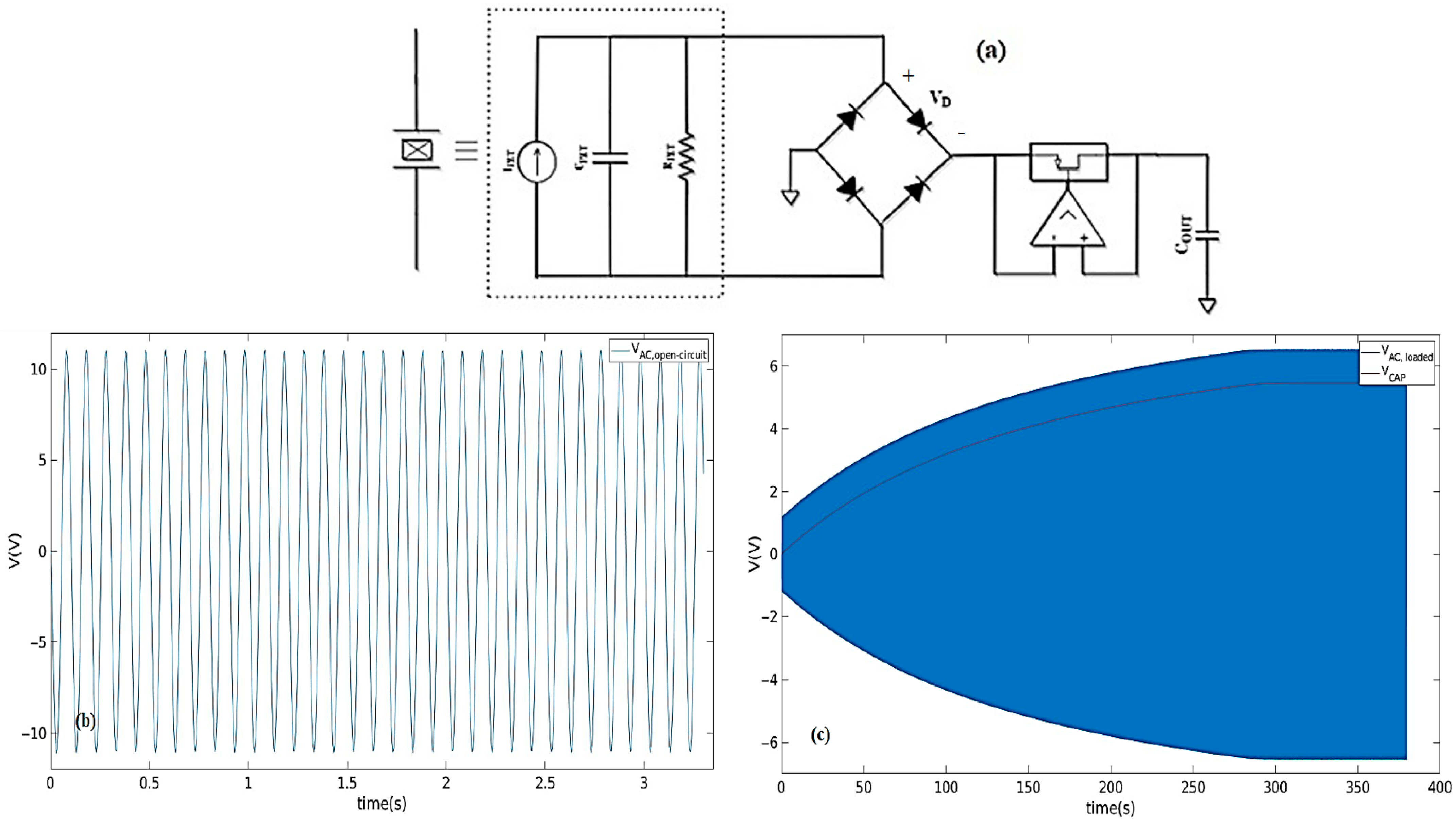
2.1. Effect of Energy Harvesting on Sensing

While simultaneous sensing and harvesting from one piezoelectric element seem to be an attractive idea for autonomous wireless sensors due to cost-effectiveness and the simplification of the design process, there are some factors that can become detrimental to the sensing process and need to be addressed.
The most important obstacle of using such a system to extract information is the effect that the harvesting process (i.e., storage capacitor voltage) has on the output signal of the piezoelectric transducer, which possesses information on various dynamic mechanical variables. Whether the output of the piezoelectric equivalent circuit or an actual piezoelectric material is used to provide energy to an energy harvesting circuit, the outcome seems to be the same: distortion of the initial (open circuit) voltage signal related to the storage capacitor’s dynamic states when the harvesting of its energy occurs (Figure 1). The term “interference” is adopted here, similarly to [15], to describe the above effect of the energy-harvesting process on sensing.
According to [15,16], the input waveform of the piezoelectric transducer when loaded (i.e., by a full-wave rectifier) is clamped to:
V A C , l o a d e d ( m a x ) = ± ( V C A P + 2 V D )
where VAC,loaded is the amplitude of the input signal when the piezoelectric element is attached to a full-wave rectifier, VCAP is the rectified voltage on the output capacitor and VD is the voltage drop on the diode.
In Figure 1c the interference phenomenon is apparent where the voltage on the storage capacitor, due to the use of a full-wave rectifier, has a direct impact on both the positive and the negative signal of the piezoelectric transducer.
Moreover, as has been previously mentioned in [15], in a sensing and energy harvesting system that would be autonomous and thus self-supplied by the storage capacitor, the loading effect on the capacitor should also be taken into consideration, since it would distort the rectified voltage, which in turn would further modify the piezoelectric output in an inconsistent way, depending on the circuitry supply demands.

2.2. Related Work in Literature

Several variations of systems exist in the literature that employ the same piezoelectric element output signal for both harvesting and sensing. Such systems apply different methods to take advantage of the dual-purposed transducer: a time-multiplexing operation associated to the different energy levels, meaning that when sufficient energy exists, the piezoelectric signal is disconnected from the energy harvesting chain and the sensing process begins until the stored energy drops below a preset threshold [11]; algorithms to minimize the distortion effect of harvesting on the sensing signal by filtering out the storage capacitor voltage [12]; event-driven operation of the transmitter that is related to its energy demands when a threshold is surpassed [13,14]; and extracting data by sampling and analyzing voltage and current signals from various points of the harvesting circuit to determine the optimal approach for data extraction [15]. A significant number of works in literature resort to two separate piezoelectric materials to achieve both sensing and harvesting to avoid compromising the reliability of a dedicated sensor.

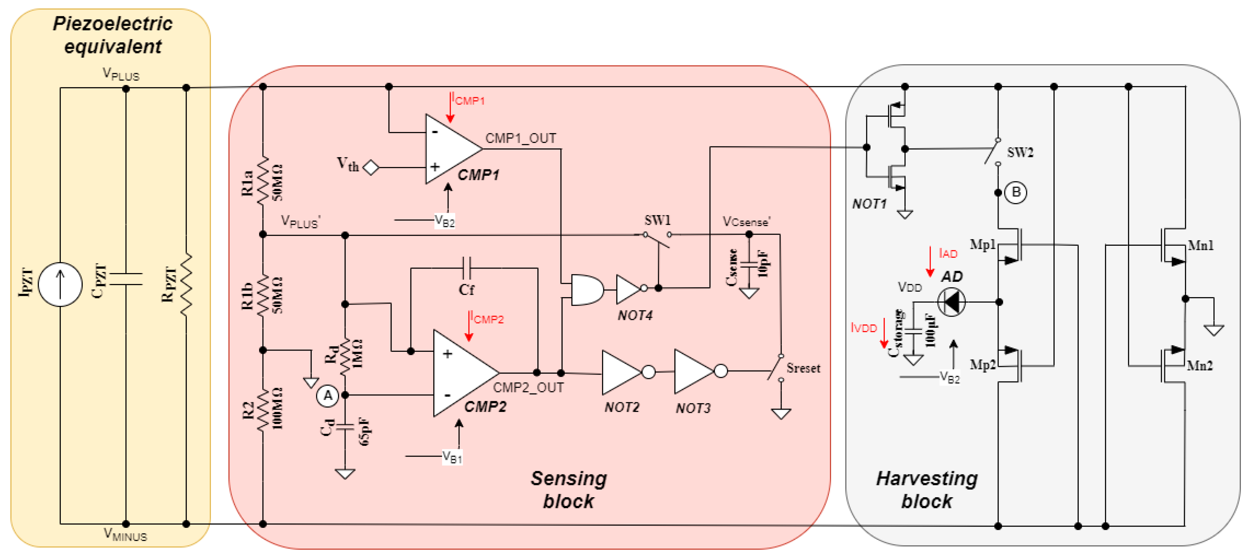
2.3. Proposed System Architecture

In this work, an interfacing circuit that makes signal filtering unnecessary, previously used in [12], while also allowing the selective measurement of the input signal regardless of the energy levels, expanding the idea of time-multiplexing in [11], was designed. The main objective of the examined application was to create a sensor interface that can be potentially employed in applications that estimate the weight of overloaded vehicles. Previous works on this subject achieve this estimation by measuring the axle load of each passing vehicle. Due to the need for a system that senses most of the intermittent signals it interfaces, and not characterize the magnitude of continuous vibrations, the proposed circuit situationally employs part of the signal for sensing and the rest to charge a storage capacitor up to a certain voltage; after that, this voltage is easier to be maintained since all signals contribute to energy storage. The designed circuit interface offers an integrated solution that is easily implemented using discrete components too. It manages to produce a sensing signal in all its integrity, unaffected by the distortions caused by the energy harvesting process. Moreover, the rest of the signal energy is used to supply its internal circuitry from the same piezoelectric element. The signal provided for further processing is available for detailed measurements since it is basically the open-circuit voltage of the piezoelectric transducer. Additionally, the circuit is very low-power, with a total power consumption of 1.02 μW, making the self-startup process possible even in small energy content applications.
This was achieved by selecting the time interval of the piezoelectric signal that is desirable for sensing, by comparing it to a threshold voltage and decoupling this signal for this time interval from the harvesting chain. Furthermore, circuitry that interacts with the signal or is directly supplied from it for this time slot was designed to draw a negligible current, thus providing large loading on the output of the piezoelectric transducer compared to its intrinsic impedance, practically unimpacting on the open-circuit voltage. More specifically, when the piezoelectric transducer is used as a sensor, it interfaces a very low-powered inverter consisting of resistive transistors and gate impedances of comparators.
An advantage of this work, when compared with the existing literature, is that it allows selective sensing of the signal in one period, offering additional control on the type of measurement that needs to be conducted in an application. In addition, the selective sensing performed by this circuit is independent of the energy levels of the storage capacitor—provided the supply voltage on the storage capacitor has reached its final value—as opposed to [11], where only periodical measurements are possible and are strongly dependent on the energy levels; in these measurements, no control over the time interval that is measured is feasible, since the whole period of each vibration is sensed. In addition, when no sufficient energy is available to power the circuit in [11], several incoming signals are left out from the sensing process.
In [12], the incoming piezoelectric signal is affected by the harvesting, thus interference caused by the energy states of the storage capacitor is not avoided. The solution presented in this work includes the extraction of the piezoelectric signal in its original pattern after filtering out the effect of the storage capacitor; this was achieved by a filtering algorithm performed using an Arduino board. However, only the pattern of the initial signal remains undistorted while information on its amplitude is lost. Therefore, our system manages to eliminate distortion of the piezoelectric signal on a circuit level, and no external microcontroller needs to be equipped for the extraction of this signal. In [13], the energy produced by the piezoelectric signal is utilized for sensing, therefore no attempt to eliminate the interference phenomenon was made.
This approach in the implementation of both sensing and harvesting, and the methods this work utilizes to achieve that, could inspire solutions to applications besides sensing that require the open voltage of the piezoelectric transducer to remain intact (e.g., maximum power point tracking using the peak value of the open voltage), while the energy provided by the transducer is harvested simultaneously.
As described thoroughly below, the output signal this circuit produces for sensing is a time-slot of the initial piezoelectric signal, and therefore it can be used for specific applications. However, since the idea of separating the sensing signal from the harvesting process is presented, modifications and adjustments on the conditions that create the desirable-for-sensing time slot could expand the range of applications that this circuit can cover.
Due to the chip area and pad number availability limitations, only the sensing block of the circuit was integrated on an MPW chip. System evaluation was conducted using a discrete implementation of the harvesting part of the circuit, combined with the integrated part in a simulated overload measurement application. In addition, simulations are provided to demonstrate the efficiency of the complete circuit. Even though the integration of the total circuit on the chip was not feasible due to silicon area limitations, post-layout simulations of the whole system prove that the total consumption is very low, rendering the circuit a viable option in applications where very low energy levels are available.

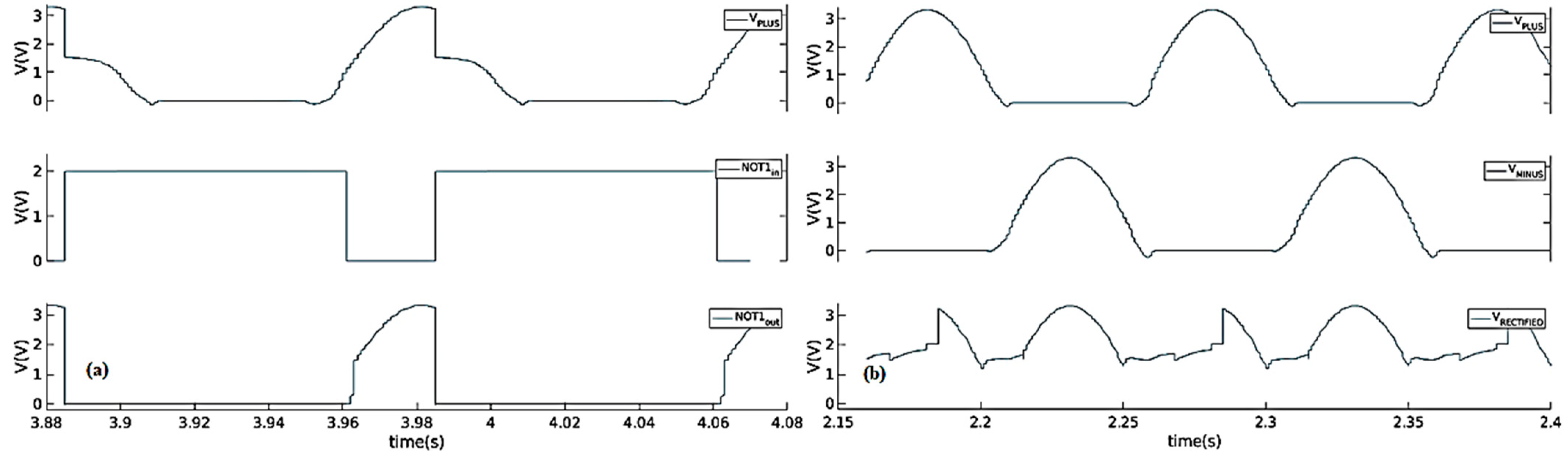
3. Proposed Circuit Analysis

In Figure 2 the total circuit is depicted. It can be divided into three basic blocks; the piezoelectric equivalent circuit, the sensing block with its corresponding control circuitry, and the energy harvesting block, which consists of the AC-DC rectifier and its control scheme.
Taking into consideration that a mass passing over a piezoelectric material at a certain speed causes the piezoelectric material to produce a voltage signal proportionally related to its weight, the piezoelectric signal can be used to measure this quantity when it is not attached to a load.
To evaluate the performance of the circuit, the piezoelectric equivalent circuit was employed, and its condition when a mass passes over it was emulated by a sinusoidal function, VPLUS (Figure 3a). VPLUS’, which is the divided version of VPLUS, is also depicted; the purpose of the VPLUS division is described in Section 3.1.
According to previous experimental works that examined this specific application [4,17,18,19], the weight W is proportional to the area under the signal curve [18,19]:
W = a u L t 1 t 2 x ( t ) d t
where L is the sensor width, u is the speed of the vehicle, x(t) is the load voltage signal, t1 is the moment VPLUS surpasses Vth, t2 the moment VPLUS falls below Vth, and a is the calibration factor. The above equation leads to the conclusion that the signal curve generated from the piezoelectric transducer should remain intact to properly measure the weight. Additionally, an adequate number of sampling points of the signal should be obtained in order to have a good estimation of the area underneath the curve.
A non-ideal WIM sensor does not recover completely and quickly enough after load excitation in order to be ready to accept the next signal. Thus, taking into consideration that the signal it generates, after it reaches its peak value, is affected until the physical structure of the sensor is completely restored to its initial state (Figure 3b), a suggested solution is to select the first half-portion of the signal for weight computation (i.e., up to the peak) [19]. This portion should later be doubled to provide a measurement of the total area under the curve. This approach is adopted in this work.

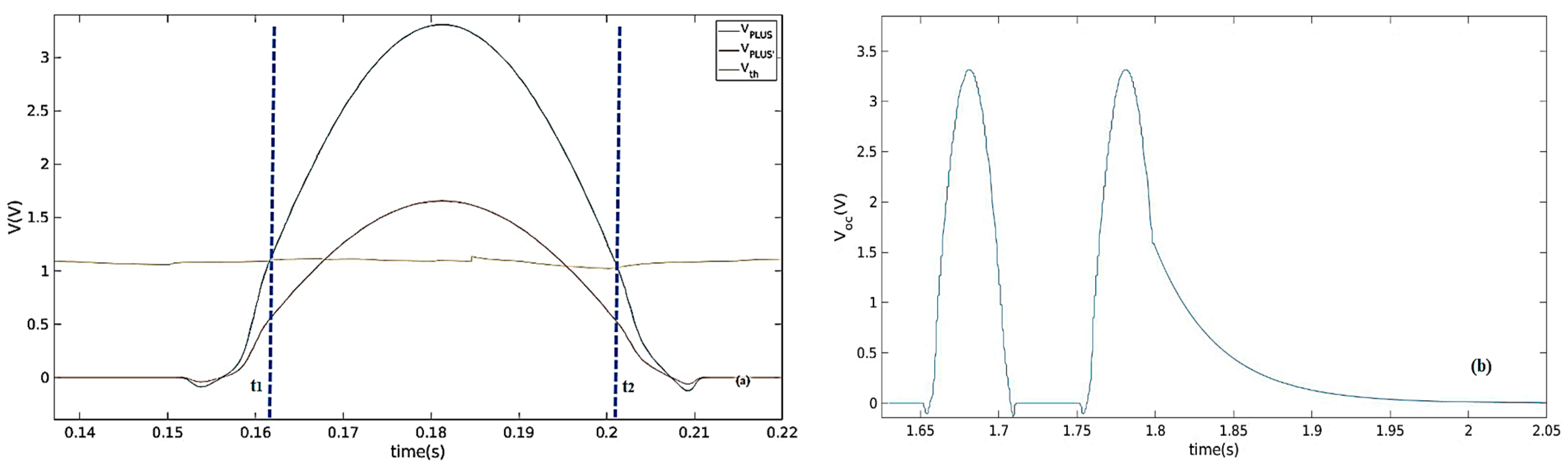
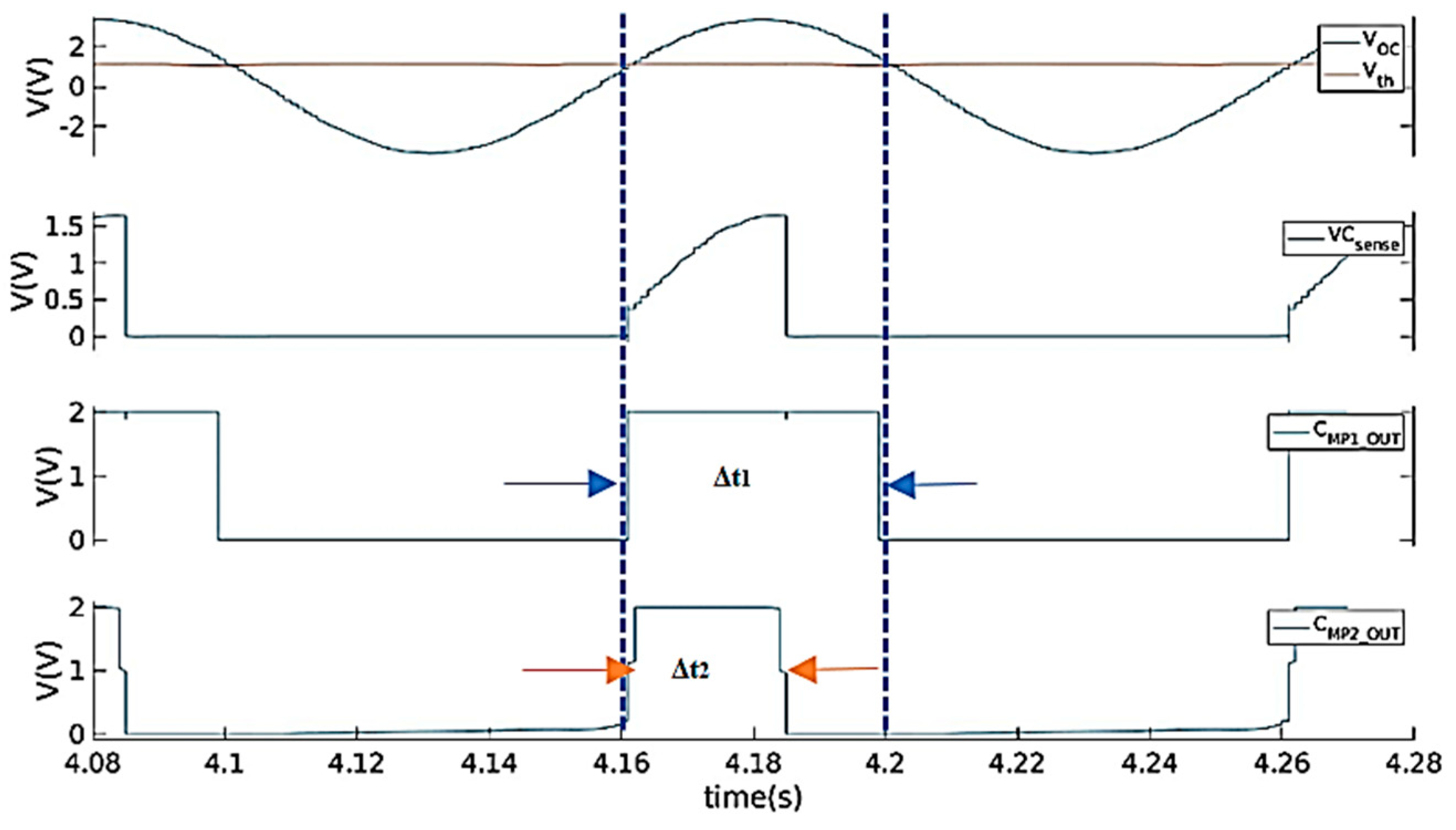
3.1. Sensing Process

Figure 2 graphically illustrates the main operation of the sensing part of the circuit.
A piezoelectric material generates electric potential proportional to the applied strain, and the polarization of the generated electricity corresponds to the direction of the induced deformation, producing alternating voltage (AC). A sinusoidal function, VOC (Figure 4), generated from the piezoelectric equivalent when it is unloaded, was employed as the examined open-circuit voltage: the positive half-period simulates the excitation of the transducer when a mass crosses it and provides information on the weight of the mass.
As explained before, in order to measure the weight of overloaded vehicles, the part of the piezoelectric signal that was selected for sensing was the open-circuit positive signal over the time difference Δt2 between the crossing of the threshold voltage and the peak voltage, as depicted in Figure 4.
The positive open-circuit piezoelectric signal, VPLUS, is compared in the comparator CMP1 to a reference voltage, Vth, that is regulated externally. This voltage corresponds to the maximum allowed weight that a load passing over the transducer should have; it can be determined after the characterization of the sensor by studying an adequate number of area data provided by the circuit, and deriving the maximum allowed voltage value of the underweight vehicles. In real operating conditions, Vth would be generated either by a simple voltage divider (externally or internally) with resistors in the order of MΩ to draw negligible current from VDD, with the objective of creating the desirable reference voltage from a regulated voltage or, alternatively, using a reference voltage supplied by VDD with highly resistive transistors that consume only a small amount of energy. An alternative external solution is to use a very low-power LDO (TPS7A02, Texas Instruments, Dallas, USA) also supplied by the storage capacitor voltage, VDD, which for a wide input voltage range would produce a specific output voltage, consuming as low as 20 nA. The output signal of CMP1 is combined with the output signal of the peak detector control switch SW1. SW1 allows the small capacitor Csense to be charged from the piezoelectric output signal only for the time interval that VPLUS > Vth until the signal reaches its peak value. The voltage on Csense is the signal that is subsequently sampled for weight estimation. The VB1 and VB2 voltages marked in Figure 2 are bias voltages of comparators CMP1, CMP2 and the comparator of the active diode AD. During the start-up process, these voltages gradually increase to reach their predetermined values whilst the circuitry they bias begins to operate. It should be noted that when they reach their final values, they bias the circuits, so that the latter draw small currents from the storage capacitor, resulting in minimum consumption.
For the control circuitry design, low-voltage devices were used in order to save the silicon area on the chip. The purpose of the external voltage divider, comprising R1a and R1b, was to obtain a fraction of the positive half-period input signal, VPLUS’; this is the signal that will be used for sensing in the WIM application. The reason why VPLUS is divided from the voltage divider is mainly that it is expected to acquire large values notwithstanding the low voltage transistors that comprise most of the circuits. As a result, only the part of the circuit that is used for the harvesting process, including comparator CMP1, was designed to withstand high voltages (open-circuit voltage signals) from the piezoelectric transducer. The rest of the circuits interface only with the divided version of the piezoelectric signal. The division factor is determined by the maximum voltage amplitudes and the minimum voltage supply the storage capacitor could provide. Since the division factor in our tested circuit was 2, to obtain a correct estimation of the area under the curve for WIM, the value of each sampled point should be doubled.
These two resistors are additionally used along with R2 to create a ground reference within the circuit, thus the relation:
R 1 a + R 1 b = R 2
must be satisfied. In addition, the divider’s resistors should have large values compared to the intrinsic impedance of the piezoelectric element, so that the minimum current is drawn (Idivider(avg) = 10.45 nA @ VDD = 2 V). In a final design, these resistors could be integrated using high-value resistors per unit area provided by the technology used.
The peak detector circuit comprises the comparator CMP2 and a delay network, Rd and Cd, which senses the peak voltage of the divided positive signal by comparing it to its delayed version in node A (Figure 2). Its output is combined with the output signal of CMP1 and control SW1 through an AND gate. A small capacitor Cf is added to the positive feedback of CMP2 to minimize the noise effect and improve the stability of the peak detector [7]. If Figure 4 is examined closely, the peak detector’s output, CMP2_OUT, is slightly off from the peak value of the initial waveform, due to the delay network of Rd and Cd that was regulated so that it creates as little delay as possible, while also remaining immune to noise. It should also be noted that the circuit operates properly in the range of input frequencies that correspond to the various speeds that the passing vehicles can have. The only part of the sensing circuit that is affected by the frequency of the incoming pulses is the detection of the peak value of VOC which is shifted from the maximum value due to the fixed values of Rd and Cd. Nevertheless, measurements in the frequency range of 1–10 Hz, corresponding to a speed up to 100 km/h, showed a maximum percentage error of peak detection of 4.1% (with 0.5% at 5 Hz) and therefore the area estimation is not affected significantly. Finally, an extra switch, Sreset, is included to discharge Csense every time the signal reaches its peak voltage, so that the sensing capacitor is reset and ready to accept the next signal.
Power switches SW1 and SW2 are bulk-regulated p-channel MOSFETs for the minimization of the leakage currents. CMP1 was designed using only high-voltage MOSFETs (VDS,pmos(max) = 15 V, VDS,nmos(max) = 10 V) available from the technology, so that it can withstand the high voltage input signals (with maximum amplitude ≤10 V). The rest of the blocks were designed with 3.3 V MOSFETs, since they need to operate in a lower voltage domain.

3.2. Energy Harvesting Process

Figure 5 graphically illustrates the harvesting part of the circuit. It consists of a CMOS rectifier (Mn1, Mn2, Mp1, Mp2) [20], a switch, SW2, that impedes harvesting when the piezoelectric element operates as a sensor, and the SW2 control block. In this way, the loading effect from the storage capacitor is avoided. An active diode, AD, was added before Cstorage to ensure unidirectional current flow towards the storage capacitor.
Every input signal with a voltage level lower than the threshold voltage Vth is rectified in the CMOS rectifier, and the storage capacitor is charged. In addition, input signals with voltages higher than the threshold voltage are rectified from the moment they reach their peak value onward, contributing to the energy accumulation on the storage capacitor. At this point, it is crucial that for the time interval Δt2 (Figure 4), Cstorage is not allowed to be charged from CPZT. It should be noted that the harvesting part of the circuit was designed using exclusively high-voltage MOSFETs.
Figure 6a depicts the input and output voltages of control inverter NOT1 (INOT1(avg) = 0.1 nA @ VPLUS(max) = 3.3 V), where it is clearly shown that switch SW2 is open during the sensing interval. The voltage on a small storage capacitor—for demonstration purposes—is illustrated in Figure 6b. This shows that for a sinusoidal signal from the piezoelectric element, only the voltages that are lower than Vth are rectified on it, in addition to the second half of the positive piezoelectric signal—after reaching the peak—that is not intended for measurement.
In order to increase the efficiency of the integrated AC-DC rectifier, high-voltage MOSFET transistors with rather large widths (3000 μm/2.9 μm) were utilized for Mn1, Mn2, Mp1, Mp2. These MOSFETs’ layouts occupy a large amount of area in the chip, and since the available space in the integrated circuit was limited, it was decided to realize the rectifier and its control circuitry externally during testing. More details are provided in Section 4.

3.3. Start-Up Process

It is demonstrated (Figure 2) that, despite the control circuits’ inactivity at the beginning of their operation, an open path for CPZT to charge Cstorage is available, since all power switches are normally turned on (p-channel MOSFETs). Moreover, to assist the start-up operation of the circuit, all circuits were designed to be biased by voltage bias circuits (Figure 7b), which, as the storage capacitor is charged, gradually reach their correct voltage value in order to properly bias the corresponding circuits (Figure 7a). Their main performance characteristic is the very low current consumption that has an average value of 29 pA and 31 pA for the voltage biases of 0.3 V and 1 V, respectively, as well as their stability over temperature and supply voltage variations.

3.4. Simulation Setup and Experimental Results

The whole circuit, including both the sensing and the harvesting parts, was designed and tested using the Cadence software, by conducting pre- and post-layout simulations, including PVT corner analysis; the circuit was successfully self-supplied, and the sensing process was executed as expected—a correct separation of the signal desirable for sensing from the harvesting process.
The main parameters of the piezoelectric element and the circuit are listed in Table 1. In Table 2, the values of the simulated voltages of Figure 2 are presented. In Table 3, the current consumption post-layout simulation results of the total sensing and harvesting system and the total power consumption are shown.

4. Proof of Concept—Weigh-in-Motion Case Study

An implementation of the circuit using only discrete components for the harvesting block (Figure 8a) and an integrated system on the chip for the sensing block (Figure 8b) was used as a proof of concept; the total circuit operated as expected. The main reason that the harvesting part was selected to be external was that the proper operation of the CMOS rectifier with high efficiency was certain, due to its design simplicity, and negligible discrepancies between the post-layout simulations and the chip implementations were expected, as was previously presented in [21]. However, confirmation of the correct interfacing of the actual piezoelectric transducer by the sensing part was crucial, since it is the essence of the proposed work.
Oscilloscope measurements showcased the correct operation of the circuit and the expected isolation of the input signal from the harvesting process when the threshold voltage was surpassed. Table 4 includes the measurement setup parameters.
Figure 9a depicts the measurements of the sensing block. VCsense is basically the voltage waveform that will provide context data on the weight of the passing load. This voltage should be sampled, and a calculation of its area will offer an estimation of the weight that passes from the piezoelectric sensor. This should be preferably done by a microcontroller that will collect a specific number of points from the VCsense waveform when CMP2_OUT is high, and will process them to calculate the area under the curve.
The positive signal has a peak value of 3 V; the effect of harvesting is visible in the second half after the peak. Since no voltage divider was necessary due to the low voltage levels of the input signal, the same voltage also appears on Csense. Figure 9b,c depict the control signals of the harvesting part. Figure 9d shows the storage capacitor charging, along with the input positive signal. The signal in Figure 9d was generated from an actual piezoelectric transducer cantilever type from MIDE. The excitation has been achieved by periodical (frequency~5 Hz) surface tapping. The cantilever was utilized in lab measurements in order to test the circuit with an actual piezoelectric element and determine whether its output power range is adequate for the circuit to be self-supplied. However, the piezoelectric transducer that would be used in the experimental weigh-in-motion application would produce a sinusoidal-like waveform, similar to that depicted in Figure 9a, when a load passes over it [17,18].
In order to quantify the accuracy of the sensing process, the peak voltage of the input signal was selected to be measured. During these measurements, the circuit was self-supplied from the storage capacitor. VPLUS(peak) is the peak value of the positive input signal and VCsense is the peak value that appears on the sensing capacitor Csense. In order to test the circuit to its limits, a signal with a maximum voltage of 4 V (the absolute maximum the low-voltage transistors can withstand) was given as the input. The results on peak detection accuracy are presented in Figure 10.
Additional measurements were conducted to test the consumption of the total hybrid circuit and consequently confirm that even in this form, the circuit can be self-sustainable. The total circuit was supplied from the storage capacitor, and its performance was tested under various harvesting conditions while the sensing process was ongoing. The piezoelectric cantilever was employed to produce the input signal. The output power was calculated from the voltage on the storage capacitor, VDD, and the current the circuit draws from the storage capacitor. In consequence, the efficiency measured corresponds to the total circuit efficiency. The results are presented in Figure 11.
The efficiency of the total circuit ranged from 56–78% for the hybrid (integrated and discrete) implementation.
An integrated version of the total sensor interface would present a higher efficiency, since the integrated CMOS rectifier [21] presents lower losses than the diode-based bridge used in the discrete implementation. This is due to the lower power losses (the large width of MOSFETs leads to smaller on-resistances of switches) and lower voltage drop of each MOSFET.
Prior works on the design of integrated AC-DC converters with high efficiency (~90%), as described in [21], show that a completely integrated solution would indeed operate properly even when lower power levels are available.

5. Conclusions

This paper introduces a very low-power integrated self-supplied self-starting piezoelectric sensor interface that utilizes the same piezoelectric transducer for sensing and energy harvesting to power its own operation. The main purpose is to demonstrate that the duality of a piezoelectric transducer can be exploited to simplify measurement circuits and optimize the utilization of the available energy. A combined discrete and integrated implementation of the sensor was examined in an overload measurement application as a proof of concept, and its self-sustainability for a wide input power range was confirmed. The circuit is highly flexible and can be adjusted to satisfy the specifications of various power level applications and piezoelectric materials.
A future goal is to fully integrate the proposed circuit on a chip and provide measurements of the final system, to showcase its feasibility and its actual potential in threshold-based sensing applications.

Author Contributions

Conceptualization, Z.A. and S.S.; methodology, Z.A.; validation, Z.A. and V.K.; writing—original draft preparation, Z.A.; writing—review and editing, Z.A., V.K. and S.S.; supervision, S.S. All authors have read and agreed to the published version of the manuscript.

Funding

This research has been co-financed by the European Regional Development Fund of the European Union and Greek national funds through the Operational Program Competitiveness, Entrepreneurship and Innovation, under the call RESEARCH—CREATE—INNOVATE (project code: T1E∆K-00360).

Acknowledgments

The authors would like to thank the anonymous reviewers for their constructive comments, which helped to improve the manuscript quality. The authors would like to also thank K. Kozalakis for his assistance regarding the system measurements.

Conflicts of Interest

The authors declare no conflict of interest.

References

  1. Motlagh, N.H.; Mohammadrezaei, M.; Hunt, J.; Zakeri, B. Internet of Things (IoT) and the Energy Sector. Energies 2020, 13, 494. [Google Scholar] [CrossRef] [Green Version]
  2. Oh, T.; Islam, S.K.; Mahfouz, M.; To, G. A Low-Power CMOS Piezoelectric Transducer Based Energy Harvesting Circuit for Wearable Sensors for Medical Applications. J. Low Power Electron. Appl. 2017, 7, 33. [Google Scholar] [CrossRef] [Green Version]
  3. Hassan, A.; El-Shaboury, A.; Mohamed, K.; Askar, M.; Mowafy, O.; Mosaad, Y.; Hassan, A.H.; Mostafa, H. A high-efficiency piezoelectric-based integrated power supply for low-power platforms. Microelectron. J. 2020, 102, 104824. [Google Scholar] [CrossRef]
  4. Xue, Y.B.; Yang, B.; Peng, L.Z.; Sun, Y.Q. Research on WIM Technology Using Cement-Based Piezoelectric Sensor. In Proceedings of the 2009 First International Conference on Information Science and Engineering, Nanjing, China, 26–28 December 2009. [Google Scholar]
  5. Jiao, P.; Egbe, K.-J.I.; Xie, Y.; Nazar, A.M.; Alavi, A.H. Piezoelectric Sensing Techniques in Structural Health Monitoring: A State-of-the-Art Review. Sensors 2020, 20, 3730. [Google Scholar] [CrossRef] [PubMed]
  6. Feng, T.; Aono, K.; Covassin, T.; Chakrabartty, S. Self-Powered Monitoring of Repeated Head Impacts Using Time-Dilation Energy Measurement Circuit. IEEE Trans. Biomed. Circuits Syst. 2015, 9, 217–226. [Google Scholar] [CrossRef] [PubMed]
  7. Romani, A.; Filippi, M.; Tartagni, M. Micropower Design of a Fully Autonomous Energy Harvesting Circuit for Arrays of Piezoelectric Transducers. IEEE Trans. Power Electron. 2013, 29, 729–739. [Google Scholar] [CrossRef]
  8. Nabavi, S.; Zhang, L. T-Shaped Piezoelectric Structure for High-Performance MEMS Vibration Energy Harvesting. J. Microelectromechanical Syst. 2019, 28, 1100–1112. [Google Scholar] [CrossRef]
  9. Kaur, B.; Agnihotri, A.; Thapar, D.; Arora, N. Piezoelectric Energy Harvester Design and Power Conditioning with Solar Integration. In Proceedings of the 2019 3rd International Conference on Electronics, Materials Engineering & Nano-Technology (IEMENTech), Kolkata, India, 29–31 August 2019; pp. 1–6. [Google Scholar]
  10. Nabavi, S.; Zhang, L. Nonlinear Multi-Mode Wideband Piezoelectric MEMS Vibration Energy Harvester. IEEE Sens. J. 2019, 19, 4837–4848. [Google Scholar] [CrossRef]
  11. Chew, Z.J.; Ruan, T.; Zhu, M.; Bafleur, M.; Dilhac, J.-M. Single Piezoelectric Transducer as Strain Sensor and Energy Harvester Using Time-Multiplexing Operation. IEEE Trans. Ind. Electron. 2017, 64, 9646–9656. [Google Scholar] [CrossRef] [Green Version]
  12. Ma, D.; Lan, G.; Xu, W.; Hassan, M.; Hu, W. SEHS: Simultaneous Energy Harvesting and Sensing Using Piezoelectric Energy Harvester. In Proceedings of the 2018 IEEE/ACM Third International Conference on Internet-of-Things Design and Implementation (IoTDI), Orlando, FL, USA, 17–20 April 2018; pp. 201–212. [Google Scholar]
  13. Jung, B.C.; Huh, Y.C.; Park, J.-W. A Self-Powered, Threshold-Based Wireless Sensor for the Detection of Floor Vibrations. Sensors 2018, 18, 4276. [Google Scholar] [CrossRef] [PubMed] [Green Version]
  14. Tang, Q.; He, Q.; Li, M.; Dong, C.; Xu, D.; Li, X. Wireless Alarm Microsystem Self-powered by Vibration-threshold Triggered Energy-harvester. IEEE Trans. Ind. Electron. 2015, 63, 1. [Google Scholar] [CrossRef]
  15. Sandhu, M.M.; Geissdoerfer, K.; Khalifa, S.; Jurdak, R.; Portmann, M.; Kusy, B. Towards Energy Positive Sensing using Kinetic Energy Harvesters. In Proceedings of the 2020 IEEE International Conference on Pervasive Computing and Communications (PerCom), Austin, TX, USA, 23–27 March 2020; pp. 1–10. [Google Scholar]
  16. Rincon-Mora, G.A. Miniaturized energy-harvesting piezoelectric chargers. In Proceedings of the Proceedings of the IEEE 2014 Custom Integrated Circuits Conference, San Jose, CA, USA, 15–17 September 2014; pp. 1–18. [Google Scholar]
  17. He, H.-L.; Wang, Y. Simulation of piezoelectric sensor in weigh-in-motion systems. In Proceedings of the 2015 Symposium on Piezoelectricity, Acoustic Waves, and Device Applications (SPAWDA), Jinan, China, 30 October–2 November 2015; pp. 133–136. [Google Scholar]
  18. Loo, F.J.V.; Visser, G. Vehicle for Dynamic Calibration of a Multiple Sensor Weigh-in-Motion System. In Proceedings of the Fourth International Conference on Weigh-In-Motion, Taipei, Taiwan, 20–23 February 2005. [Google Scholar]
  19. Kwon, T.M. Signal processing of piezoelectric weight-in-motion systems. In Proceedings of the Fifth IASTED International Conference on Circuits, Signals and Systems (CSS ’07), Anaheim, CA, USA, 25–29 March 2007; ACTA Press: Calgary, AB, Canada, 2007. [Google Scholar] [CrossRef]
  20. Wahab, N.A.; Salleh, M.K.M.; Othman, N.; Khalid, M.F.A.; Hidayat, N.M. High efficiency CMOS rectifier for energy har-vesting. In Proceedings of the IEEE Industrial Electronics and Applications Conference (IEACon), Kota Kinabalu, Malaysia, 20–22 November 2016. [Google Scholar] [CrossRef]
  21. Kosmadakis, I.; Konstantakos, V.; Laopoulos, T.; Siskos, S. An automated measurement bench for vibration-based energy harvesting systems. In Proceedings of the 2013 IEEE 7th International Conference on Intelligent Data Acquisition and Advanced Computing Systems (IDAACS), Berlin, Germany, 12–14 September 2013; Volume 1, pp. 15–20. [Google Scholar]
Figure 1. (a) Full-wave rectifier with piezoelectric equivalent input (b) piezoelectric open-circuit voltage and (c) effect of the storage capacitor voltage on the input waveform.
Jlpea 11 00027 g001
Figure 2. Proposed sensing and harvesting interface from a piezoelectric transducer.
Jlpea 11 00027 g002
Figure 3. (a) Generated piezoelectric waveform VPLUS due to moving mass (simulation) and its divided version VPLUS’. (b) A severe case of a piezoelectric recovery problem is visible on the second peak—qualitative approach.
Jlpea 11 00027 g003
Figure 4. Waveforms of the sensing part of the circuit.
Jlpea 11 00027 g004
Figure 5. Harvesting part of the circuit with a control.
Jlpea 11 00027 g005
Figure 6. (a) Control signals in harvesting part. (b) Positive (VPLUS), negative (VMINUS) piezoelectric signal and rectified voltage (VRECTIFIED) on a 10 pF output capacitor.
Jlpea 11 00027 g006
Figure 7. (a) Start-up: circuits gradually begin to turn on as the storage capacitor is charged. (b) Voltage bias circuits.
Jlpea 11 00027 g007
Figure 8. (a) Setup for the discrete implementation. (b) Integrated circuit of the sensing part (Area on chip: 0.53 × 0.62 mm2).
Jlpea 11 00027 g008
Figure 9. Measurements of the hybrid implementation. (a) Voltages of sensing block. (b) Input of inverter NOT1. (c) Output of inverter NOT1. (d) Piezoelectric positive signal (spikes) generated from piezoelectric material and voltage (continuous line) on the storage capacitor.
Jlpea 11 00027 g009
Figure 10. (a) Peak voltage of input signal vs. peak voltage on Csense. (b) Accuracy of peak detection vs. VPLUS(peak).
Jlpea 11 00027 g010
Figure 11. Input and output power vs. Vin(rms).
Jlpea 11 00027 g011
Table 1. System parameters and specifications.
ParameterValueUnit
CPZT22nF
RPZT300
fPZT10Hz
IPZT12μA
Vth1V
Cstorage100μF
R1a50ΜΩ
R1b50ΜΩ
R2100ΜΩ
Table 2. Simulated voltages.
ParameterValueUnit
VOC(p-p)6.6V
VPLUS(peak)3.314V
VPLUS(peak)1.64V
VCsense(peak)1.638V
VDD2V
VB10.3V
VB21.0V
Table 3. Simulation results.
ParameterValueUnit
IC1(avg) @ VDD = 2 V8.64nA
IC2(avg) @ VDD = 2 V1.01nA
IAD(avg) @ VDD = 2 V20.93nA
IVDD(avg) @ VDD = 2 V0.51μA
Power Consumption1.02μW
Table 4. Measurement setup.
ParameterValueUnit
fPZT 1 (frequency generator)100Hz
fPZT (piezoelectric cantilever)10Hz
Vth1V
1 Frequency value required to create a floating sinusoidal signal.
Publisher’s Note: MDPI stays neutral with regard to jurisdictional claims in published maps and institutional affiliations.

