Abstract
Modern electronic devices are an indispensable part of our everyday life. A major enabler for such integration is the exponential increase of the computation capabilities as well as the drastic improvement in the energy efficiency over the last 50 years, commonly known as Moore’s law. In this regard, the demand for energy-efficient digital circuits, especially for application domains such as the Internet of Things (IoT), has faced an enormous growth. Since the power consumption of a circuit highly depends on the supply voltage, aggressive supply voltage scaling to the near-threshold voltage region, also known as Near-Threshold Computing (NTC), is an effective way of increasing the energy efficiency of a circuit by an order of magnitude. However, NTC comes with specific challenges with respect to performance and reliability, which mandates new sets of design techniques to fully harness its potential. While techniques merely focused at one abstraction level, in particular circuit-level design, can have limited benefits, cross-layer approaches result in far better optimizations. This paper presents instruction multi-cycling and functional unit partitioning methods to improve energy efficiency and resiliency of functional units. The proposed methods significantly improve the circuit timing, and at the same time considerably limit leakage energy, by employing a combination of cross-layer techniques based on circuit redesign and code replacement techniques. Simulation results show that the proposed methods improve performance and energy efficiency of an Arithmetic Logic Unit by 19% and 43%, respectively. Furthermore, the improved performance of the optimized circuits can be traded to improving the reliability.
1. Introduction
Since the advent of electronic digital computing, relentless technology scaling has enabled an exponential improvement in computation capability while decreasing the cost and power consumption. Gordon Moore predicted in 1965 that the number of transistors in integrated circuits would double every year to address the ever-increasing demand for higher computation power [1] (this prediction was adjusted afterward to reflect the real progress [2,3]). Such continuous growth in computation capability over more than five decades affected almost all aspects of human life, including but not limited to industry, business, health-care, government, and society, which effectively started the Information Age, and made digital computing circuits an inseparable part of our everyday life.
Moore’s law has faced several technological challenges and has been slowed down in the past decade [2,4,5]; however, still more transistors can be integrated on every new technology generation down to a 3 nm node [6,7].
To avoid exponential growth in the power density, various parameters including supply voltage of digital circuits have been scaled according to Dennard’s scaling law [8]. However, the supply voltage did not scale at the same pace for about one decade (since 2005–2006) due to technological challenges associated with nanometer-scale devices [9]. Since then, various architectural and design directions have been actively explored including many-core computation, parallel processing, and 3D integration to provide more computation power [5,6,7]. However, the main challenges caused by the end of Dennard’s scaling are energy efficiency and power density, which cannot be addressed by such approaches [10,11,12]. Without proper addressing of the increasing power density due to technology scaling, it is not possible to utilize all the components of a chip at the same time due to overheating, a problem commonly known as Dark Silicon [11,13], which diminishes the benefits of scaling. Therefore, reducing the power density through improving the energy efficiency is pivotal for future digital circuits.
In fact, energy-efficient computing has already become a primary requirement in various application domains. At one end of the spectrum, the growing IoT applications, with an expected 20 billion connected devices by 2020 [14,15,16], are continually looking for more energy efficiency. These IoT devices are expected to operate on limited energy sources such as batteries or energy harvesting sources. High-performance servers and data centers, at the other end, are responsible for a significant amount of consumed electricity worldwide (about 1.4% of the consumed electricity worldwide in 2011, and growing in much faster speed compared to other electricity consumers) [17]. A large portion of the cost of data centers is directly or indirectly due to the energy consumption of digital circuits [17]; hence, it is necessary to improve the energy efficiency of high-performance computing as well.
Power consumption of digital circuits has two components: dynamic power consumption, due to circuit activity and computation, and leakage power consumption, due to slight leakage current of transistors. Reducing the power density can be achieved through various approaches such as optimizing design techniques, employing power management strategies, improving the technology, and scaling supply voltage [18]. Each of these approaches aims at reducing dynamic power, leakage power, or both. In this regard, optimizing Instruction Set Architecture (ISA), scheduling methods, pipeline design, and synthesis methodologies have already enabled vast improvements in the energy efficiency [19].
Techniques such as clock-gating and power-gating are widely used in existing digital circuits to cut down dynamic and leakage power of the idle components [20]. Dynamic Voltage and Frequency Scaling (DVFS) promotes supply voltage and speed adaptation depending on the workload to reduce power consumption under low workload [21,22].
Aggressive supply voltage reduction down to the sub-threshold region is known as an important instrument, which reduces power consumption by several orders of magnitude and improves energy efficiency [12,18,23,24,25]. Intel has demonstrated ultra-low power characteristics using such aggressive voltage scaling by its experimental IA32 processor, which can run Windows and Linux on a small solar panel [26]. In addition to extensive power reduction, voltage scaling degrades circuit speed significantly. Many applications have performance constraints that prevent them from operating in the sub-threshold region.
By operating digital circuits at supply voltages close to the threshold voltage of the transistors, which is known as NTC, it is still possible to gain very high energy efficiency and achieve enough performance for many applications in the IoT domain [27,28]. Additionally, many-core computation based on NTC is an attractive approach to improve energy efficiency while satisfying the computational demands for highly parallel workloads of data centers [10,29,30,31]. Therefore, NTC is considered an attractive paradigm for improving the energy efficiency in modern technology nodes [32], if the associated reliability challenges are addressed. These reliability challenges are typically caused by enormous sensitivity of NTC circuits to variability sources and complicate NTC circuit design and operation.
Along with the enormous energy benefits, NTC comes with a variety of design challenges. The most obvious one is the performance reduction of 10× compared to the super-threshold domain, which may limit the applicability of NTC [27]. In addition, the escalated sensitivity to variability (such as process and voltage variation) at reduced supply voltages forces designers to add very conservative and expensive timing margins to achieve acceptable yield and reliability [33].
Moreover, in the near-threshold region leakage energy becomes comparable to dynamic energy, thus approaches to minimize leakage are of uttermost importance for NTC designs. Hence, although conventional designs can technically operate in the NTC domain, due to these challenges, new design paradigms have to be developed for NTC to harness its full potential.
Data paths are core components of any processing element such as processor cores and accelerators. A data path consists of various functional units, such as Arithmetic Logic Unit (ALU) and Floating Point Unit (FPU), the timing and power consumption characteristics of which significantly impact the overall performance of the processor. Therefore, optimizing the reliability, energy efficiency, and performance of data paths is of decisive importance.
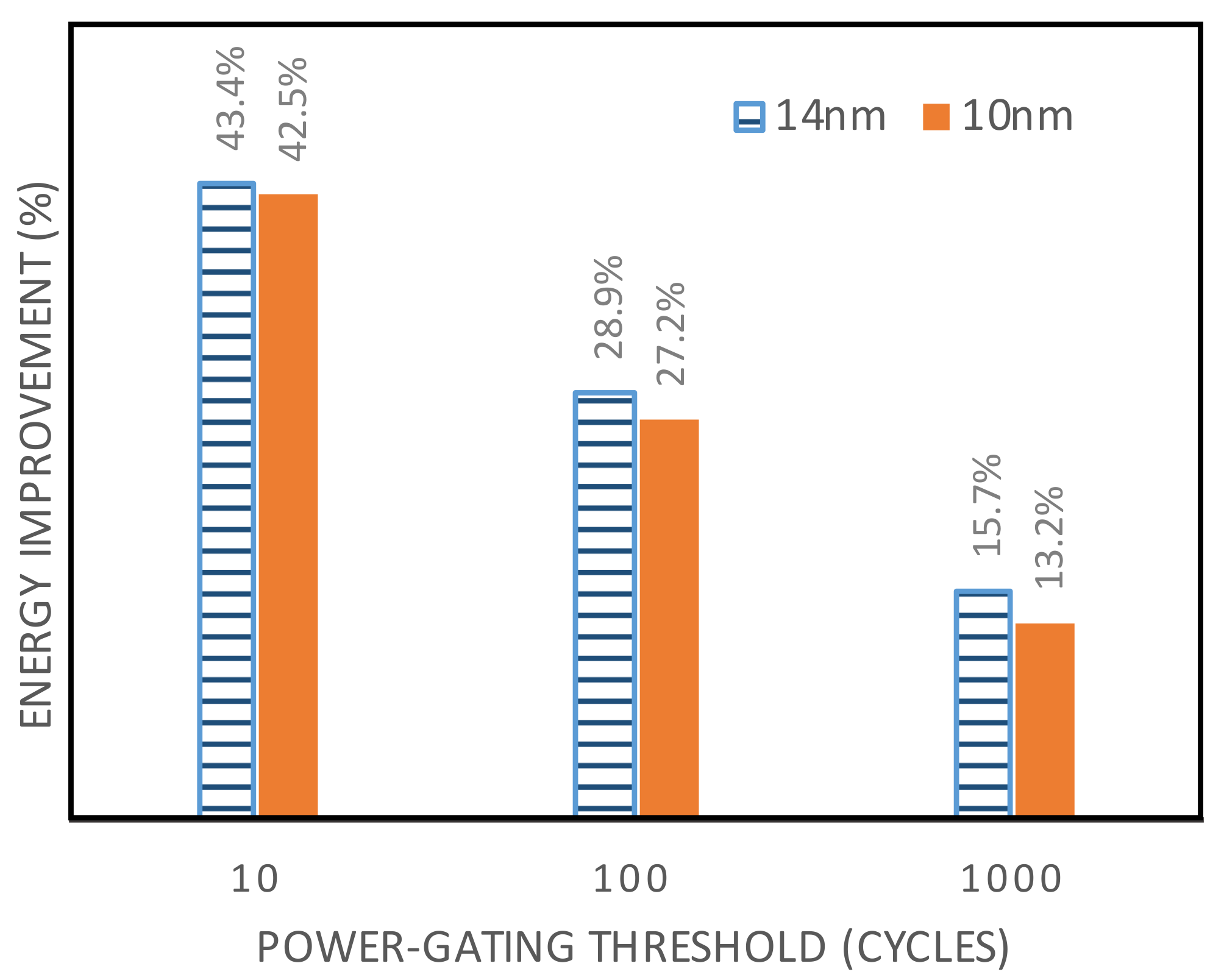
This paper presents two cross-layer functional unit optimization opportunities based on (1) instruction multi-cycling and (2) functional unit partitioning, which improve energy-efficiency, reliability, and performance. We evaluate our methodology by using an ALU implemented for Alpha ISA. Our results show that the proposed approach can effectively improve energy efficiency and reliability. For example, instruction multi-cycling effectively removes the extra timing slacks and improves the energy efficiency of a circuit by up to 34%. Furthermore, the functional unit partitioning approach can improve the energy efficiency of an ALU by 43.4% while having positive impacts on the reliability and performance as well.
The rest of this paper is organized as follows. Section 2 provides the background on near threshold computing. Section 3 reviews the state-of-the-art and their shortcomings. The optimization approaches based on instruction multi-cycling and functional unit partitioning are presented in Section 4, while Section 5 discusses the optimization results. Finally, Section 6 concludes the paper.
2. Near-Threshold Computing
Various methodologies at different abstraction-levels have been proposed and employed [18,19,20,21,22,34,35,36] to improve the energy efficiency and overcome the power wall challenge caused by the end of Dennard’s scaling [9,10,11,12]. Aggressive supply voltage scaling down to the sub-threshold region [12,18,23,24,25] is also presented as an effective way to reduce the power consumption by several orders of magnitude; however, the speed of digital circuits at that supply voltage range is poor. In the following, we present a promising approach towards supply voltage scaling, called NTC, which also retains enough performance for many applications.
Near-Threshold Computing is a paradigm in which the supply voltage is reduced close to the threshold voltage of transistors to gain large energy efficiency while retaining enough performance for many applications. However, there are various challenges towards NTC mainly in the area of reliability and energy efficiency, which can nullify the benefits of NTC if not addressed correctly. This paper focuses on the NTC and its challenges.
From a circuit-level point of view, the total power consumption of a circuit can be calculated as in Equation (1):
where , , and are dynamic switching power, dynamic short-circuit power, and leakage power, respectively.
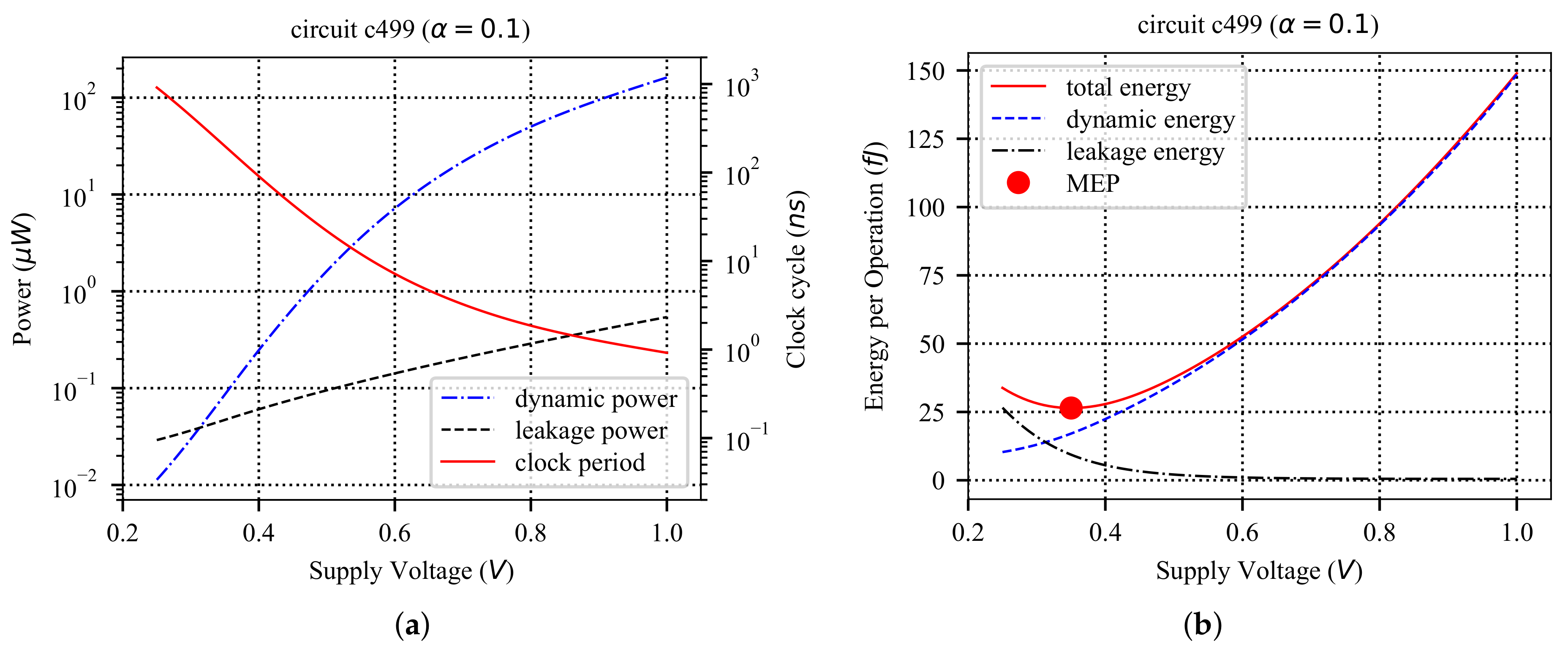
In the nominal supply voltage, the is the dominant power consumption, which is quadratically dependent on the supply voltage, as shown in Figure 1a. Therefore, reducing the supply voltage can quadratically reduce the overall power consumption. In the same supply voltage regime, the speed of a circuit is linearly dependent on the supply voltage.
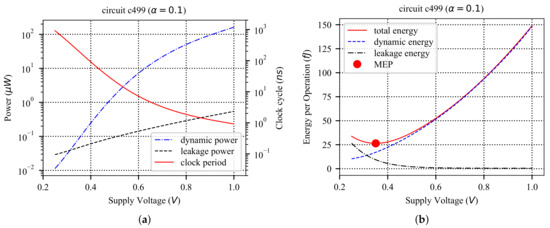
Figure 1.
MEP exploration for circuit c499 from ISCAS’85 benchmark [37,38]. (a) Circuit power and clock period versus supply voltage (); (b) Minimum Energy Point (MEP). Minimum Energy Per operation is achieved where is close to .
The energy consumption is calculated according to Equation (2):
Therefore, by slightly reducing the supply voltage from the nominal voltage, it is possible to reduce the energy consumption, linearly. As shown in Figure 1b, this energy improvement holds as long as the rate of total power consumption reduction is higher than the rate of speed degradation. When goes below , the speed degradation becomes exponential because the current has an exponential relation with supply voltage. Therefore, energy consumption starts to increase due to higher rate of speed degradation. As a result, the supply voltage leading to minimum energy consumption is somewhere close to the threshold voltage of transistors. Such operating condition leading to the best energy efficiency, i.e., the lowest energy consumption, is commonly known as the Minimum Energy Point (MEP) and is shown in Figure 1b for c499 circuit from ISCAS’85 benchmark circuits [37,38].
2.1. MOSFET Model in the Near-Threshold Voltage region
The conventional three-region long-channel MOSFET model as well as the alpha-power model [39] are piece-wise models with a discontinuity at the threshold voltage of transistors, which makes them inappropriate for NTC circuit analysis. However, it is possible to explain the characteristics of MOSFET based on continuous models such as EKV [40,41,42]. Accordingly, a simplified trans-regional model for digital NTC CMOS circuits is proposed in [43], which facilitates analytical analysis. Based on this model, the MOSFET on-current can be obtained based on the overdrive voltage as follows:
where depends on process parameters and transistor dimensions (), whereas , , and are process independent fitting parameters [43]. In the above equation, it is assumed that ; therefore, the term depending on is eliminated. However, it is possible to consider the threshold voltage dependency on and body-biasing. Based on this model, the propagation delay of a gate in the Near-Threshold Voltage (NTV) region is obtained as:
Similarly, energy and power consumption of digital circuits can be calculated in the NTV region [43].
Process, Voltage, and Temperature Variation in NTC
The impacts of process, supply voltage, and temperature variations (PVT) are more pronounced in the NTV region [27,33,44]. Authors of [45] showed that the sensitivity of the drain-source current of a transistor () to changes in and increases by about 10× when the supply voltage is reduced from the super-threshold region to the sub-threshold region. Equation (4) also demonstrates that propagation delay in the NTV region is exponentially dependent on supply and threshold voltages. Intel [33] reported that while the process and temperature variations cause 18% and 5% performance variation in the super-threshold region, their impacts aggravate to 2× performance variation in the NTV region.
The power consumption of NTC circuits is orders of magnitude smaller than the super-threshold region. As a result, runtime supply voltage fluctuation caused by power consumption also decreases by the same scale, which makes it insignificant in NTC circuits, even considering the large sensitivity to fluctuations. Moreover, the temperature of NTC circuits is solely determined by the ambient temperature since the power dissipation is very small and has a negligible impact on circuit temperature fluctuation [46].
2.2. NTC Challenges
2.2.1. Reliability
Aggressive supply voltage scaling to the NTV region has benefits and drawbacks in terms of reliability. Reducing the supply voltage to the NTV region greatly reduces internal electric fields and current density compared to the super-threshold region, which helps to protect the circuits from some aging phenomena and their associated reliability problems.
Nevertheless, the exponential sensitivity to PVT in the NTV region severely affects the circuit behavior and may lead to large performance variation or reliability issues, in terms of functional failure or timing violations. As presented in [33], performance variation is observed between different fabricated NTC cores only due to process variation, whereas this variation was limited to at the nominal voltage. Techniques such as adaptive body biasing [27] and supply voltage scaling [47] are presented to address such performance fluctuation. Similarly, the maximum clock frequency of an NTC circuit may change by due to 110 °C temperature fluctuation, while the impact of such temperature fluctuation on performance is only at the nominal voltage [33] (the measurement is done for a 65 nm typical die). An unwanted performance fluctuation at gate-level may lead to timing violations. Setup-time violations can be addressed by increasing the clock period (i.e., reducing clock speed f), which inflicts performance and energy efficiency loss. Various timing error detection and correction methods have also been proposed to address setup-time issues [48,49,50,51,52], which may be costly as the number of timing errors increases rapidly in the NTV region. However, a hold-time violation cannot be fixed by changing the clock speed and leads to a functional failure. As an example, the number of hold-time violations increases by up to 16× when operating in the NTV region compared to the nominal voltage [53]. In order to fix these timing violations, many buffers have to be inserted into the violating paths to delay the arrival times of such short paths. Therefore, the overhead of buffer insertion in the NTV region is significantly larger than that of the super-threshold region.
Reduced noise margin due to voltage scaling is a major challenge in storage component design for NTC. Conventional 6T SRAM memory cells cannot operate correctly in the NTV region without redesigning [54], and 8T or 10T SRAMs are preferred due to better noise margin and resiliency to variations [55,56,57,58]. In addition, due to low activity of memory cells, the optimum supply voltage may be considerably higher than core logic. Therefore, voltage level converters may be needed to interface memory and core cells, which brings additional complexity to routing and Power Delivery Network (PDN) design. Similarly, flip-flops have issues due to reduced noise margin and high sensitivity to variations [27,33]. Therefore, various flip-flop designs have been studied for low-voltage operation and are optimized for NTC [27,28,33,59,60,61]. The soft-error rate of storage components is dependent on the critical charge, which decreases by 5× in the NTV region [62]. Therefore, more soft-errors are observed in the NTV region in both logic and memory components. Various methods have been proposed at different abstraction levels from device to architecture-level to address the faults caused by soft-errors for NTC [63,64,65,66,67,68,69,70].
2.2.2. Energy Efficiency
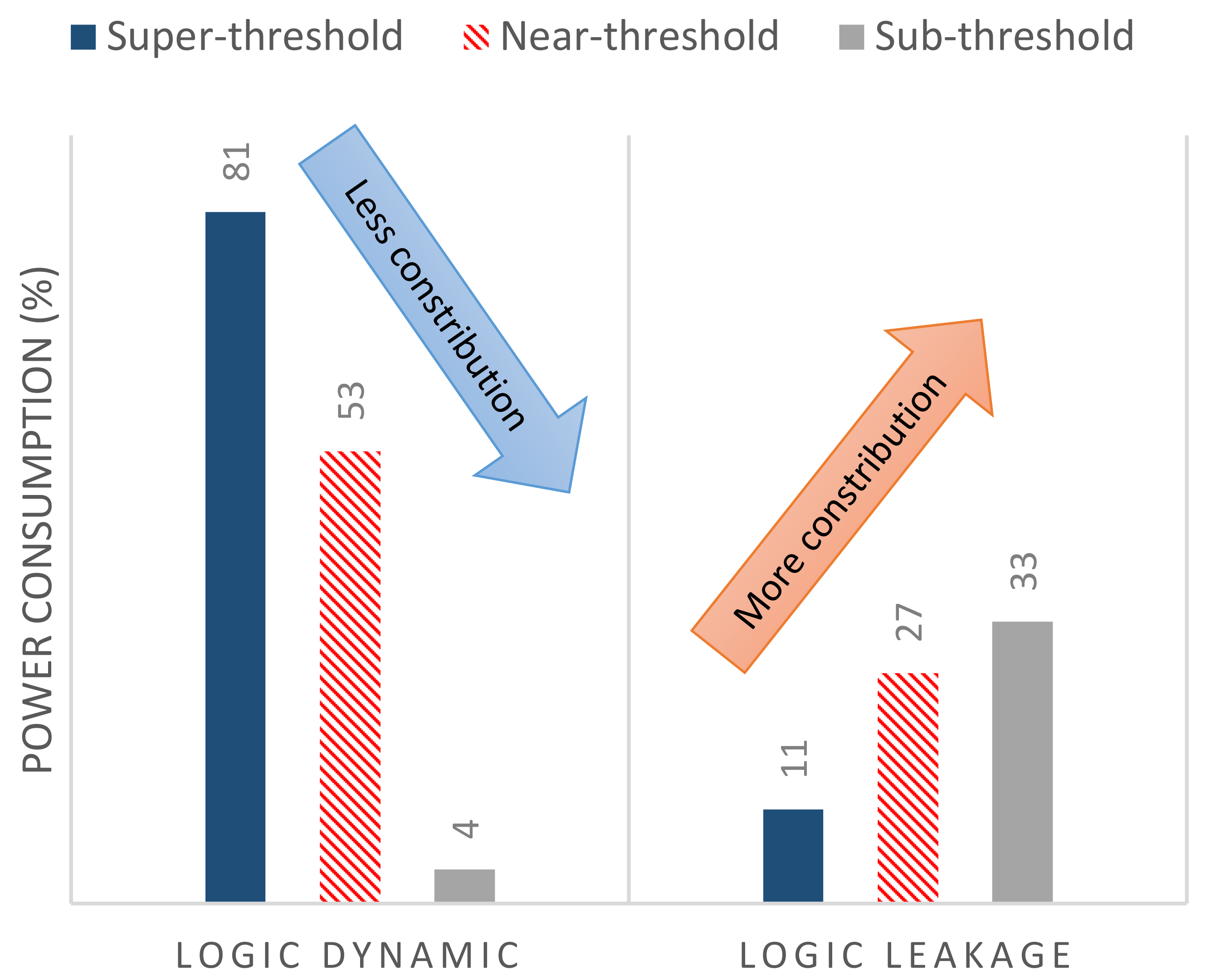
The energy efficiency of NTC circuits is highly dependent on design, process variation, and runtime parameters. Scaling down the supply voltage changes the ratio of dynamic and leakage power consumption significantly, causing a paradigm shift in design and optimization. Figure 2 presents the power consumption of an IA32 processor. The contribution of logic dynamic power decreases from 81% in the super-threshold region to 4% in the sub-threshold region, whereas the contribution of logic leakage power increases from 11% to 33% [26]. Therefore, leakage power reduction techniques at architecture-level (e.g., by power-gating schemes) down to device-level (e.g., by incorporating advanced technologies such as FinFET) are more rewarding in the NTV region compared to the super-threshold region, in which leakage power has a smaller contribution.
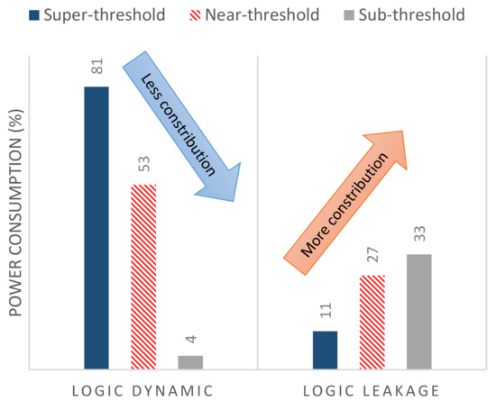
Figure 2.
Power breakdown of the IA32 processor presented in [26] highlights a significant increase in the relative contribution of the leakage power of logic components to the total power consumption, when supply voltage is reduced towards near-threshold and sub-threshold regimes. The rest of the power consumption is due to the memory (8%, 20%, and 63% in the super-threshold, near-threshold, and sub-threshold region, respectively.)
The methods used for addressing the variation-induced reliability challenges affect the energy efficiency as well. Some of the methods commonly used in the super-threshold region for controlling the impact of variations are too expensive in the NTV region. As an example, adding a timing margin to compensate for variation-induced timing fluctuation is energy inefficient in the NTV region due to the extent of variations. Therefore, it is necessary to design the circuits to be more resilient against timing variation, for example, by variation-aware circuit synthesis.
The MEP of a circuit points to a specific supply voltage and the maximum speed (inversely proportional to clock period ) at that supply voltage. A number of factors impact the MEP of a circuit including technology, internal activity, workload, and process and runtime variations. FinFET technology offers close to 60 mV/dec sub-threshold slope leading to better Ion/Ioff ratio, which is very useful in reducing the MEP and improving the energy efficiency. It has been shown that the MEP may move from a sub-threshold voltage region to super-threshold voltage region depending on the circuit structure and circuit internal switching activity [32]. For example, the contribution of leakage power to the total power, i.e., , is typically larger in SRAM arrays compared to the core logic. Therefore, the MEP of SRAM arrays is higher than core logic [32]. This also means that workloads that cause higher internal switching activity (high dynamic power), will reduce the MEP of a circuit. Process and runtime variations significantly contribute to MEP fluctuation. Therefore, design optimization and runtime tuning are also necessary to achieve high energy efficiency in the NTV region.
The average impact of process variation on of the benchmark circuits is displayed in Figure 3a. The shift in due to process variation is on average 66 mV for the benchmark circuits. This shift in may lead to significant performance variation and energy overheads. Moreover, the speed () of some circuits is also highly affected by process variation. Figure 3b demonstrates that of a circuit may change by about one order of magnitude when it is under different process variation impacts.

Figure 3.
Process variation impact on the MEP of some ISCAS’85 benchmark circuits [71]. (a) Process variation can change on average by 66 mV. (b) Process variation can change by up to an order of magnitude over different process corners.
The impact of temperature variation is shown in Figure 4, where the MEP is plotted for different temperatures ranging from to 100 °C. The clock period corresponding to the MEP () is also greatly affected by the change in the circuit temperature, with an exponential dependency. Comparing Figure 3 and Figure 4 reveals that the impact of temperature could be much stronger than the impact of the process variation. This is also in line with the reported process and temperature variation sensitivities as in [27,28,33,47].

Figure 4.
Temperature variation impact on the MEP of some ISCAS’85 benchmark circuits [71]. (a) Up to 80 mV variation in is observed over 125 C temperature change. (b) More than 2 orders of magnitude variation in is observed over 125 C temperature change.
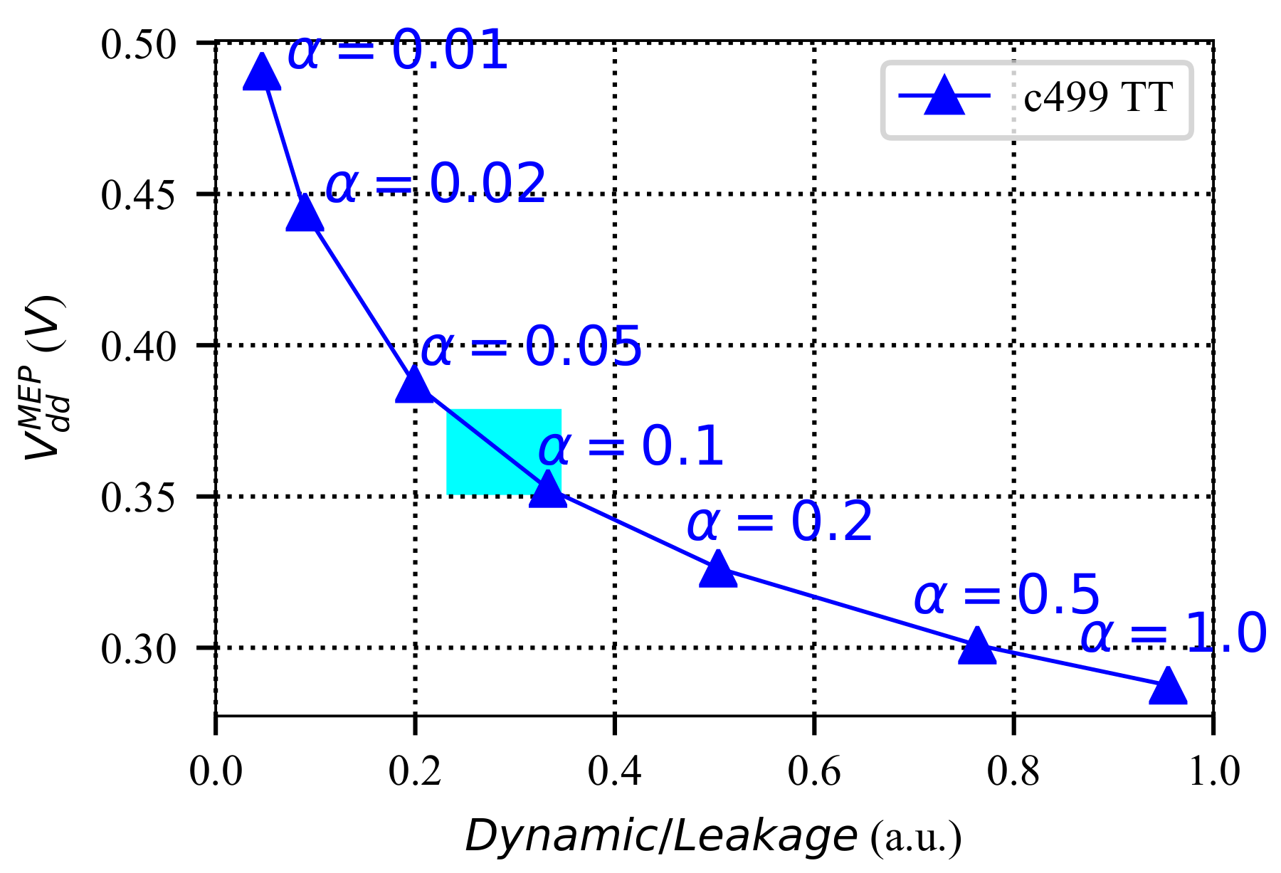
Figure 5 shows the change in for circuit c499 of ISCAS’85 benchmark due to a change in the internal switching activity. The x-axis of the figure represents the ratio of the dynamic energy to the leakage energy of the circuit (Dynamic/Leakage), when the circuit is operating at the nominal supply voltage (). The Dynamic/Leakage value has an inverse relation with as demonstrated in Figure 5. According to this figure, if the input switching activity changes from 0.01 to 0.1, the can vary from 0.49 V down to 0.35 V as Dynamic/Leakage increases. In a pure combinational circuit such as c499, the impact of workload variation could be very high as the dynamic power consumption is dependent on the input switching activity . However, in sequential circuits, a large portion of dynamic power consumption is related to the clock network. In such cases, variation due to fluctuation is typically less than in combinational circuits. Therefore, workload variation can also have a significant impact on energy efficiency, depending on the circuit architecture.
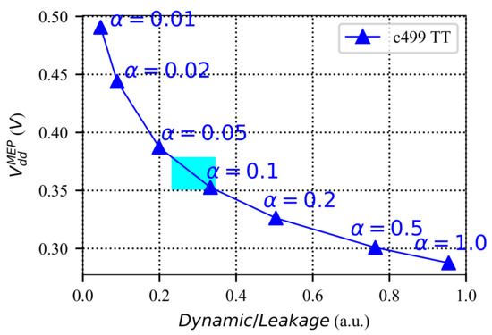
Figure 5.
Workload variation impact on the MEP. The change in the versus the ratio of dynamic to leakage energy at nominal . The realistic change in the input switching activity is displayed by the light blue box () [71].
In summary, the energy efficiency of NTC circuits is highly affected by PVT. Design optimization methods can effectively improve energy efficiency by reducing the leakage power. Runtime tuning methods can adapt the circuit to operate at the MEP, which fluctuates at runtime due to temperature and workload fluctuation.
2.2.3. Wide-Voltage Resiliency
Some NTC circuits are required to operate at different supply voltage modes, due to runtime MEP tuning, ultra-low power requirements, or speed constraints (super-threshold). When a task with specific timing constraints executes on the NTC circuit, the supply voltage may be increased to the super-threshold region to meet the performance constraints. However, this brings reliability issues associated with super-threshold voltage, such as aging, into consideration as the circuit may operate in that mode for some time. For example, an IoT edge device may be assigned to process some data within a specific amount of time and send them to an IoT gateway. Therefore, it is necessary to take the aging issues into consideration if a device is expected to operate over a wide-voltage range as this may have deteriorating impact on the device operation when it is switched back to the NTV region or even in the super-threshold voltage region.
2.2.4. Other Challenges
Static Timing Analysis (STA) tools are typically utilized to evaluate circuit timing. Conventional logic synthesis tools leverage STA to further optimize digital circuits and resolve timing issues. They rely on a corner analysis, which means that the circuit timing is evaluated for best and worst process and temperature corners. However, given the extent of variation in the NTC circuits, this approach is too pessimistic. Therefore, Statistical STA (SSTA) should be used to determine the timing of NTC circuits. Conventional SSTA tools propagate random variables, i.e., such as threshold voltage and transistor dimensions, to extract the distribution of output timing. This can be done based on Monte-Carlo analysis, which is extremely time-consuming, or analytical analysis. Based on Equation (4), given that or are statistical parameters with a normal (Gaussian) distribution, the resulting delay distribution would be log-normal [43]. Therefore, the SSTA tools used for NTC circuits may need to consider such exponential sensitivity by propagating log-normal distributions, which makes the SSTA tools quite complicated.
3. Related Work
As explained, keeping up with reliability requirements while gaining high energy efficiency is a major challenge for NTC design. Many researchers have focused on these issues to enable widespread use of NTC in various application domains. In this regard, the state-of-the-art can be divided into:
- Design flow and methodology optimization: Due to high integration and the complexity associated with circuit design in modern technologies, Electronic Design Automation (EDA) tools are extensively used to enable circuit design and optimization. Hence, efforts have been focused on improving the EDA tools for NTC. Kaul et al. [33] provided a list of challenges for NTC circuit design, from device modeling to test, and desired design technologies. Recent works have addressed some of the NTC challenges in device modeling [43,72], variation modeling [40,73,74], synthesis [75], leakage power management [75,76], and system-level modeling [77]. There are still major shortcomings in variation-aware library characterization, verification, and testing.
- Design optimization for NTC: Various methods have been proposed to improve the design for NTC, from device-level to architecture-level. At circuit-level, robust standard cell libraries [26], memories [54,56,57,58] and flip-flops [27,33] are optimized for NTC. Level shifter designs have been vastly studied for interfacing between different voltage islands [60], and clock networks are redesigned for low-voltage operation [73]. Additionally, timing error correction methods such as [49,78,79] can be used to mitigate timing variations at runtime. At architecture-level, caches [80], processor pipeline [81,82,83,84] and ISA [85] can be optimized, and other leakage power reduction methods are also investigated [26]. However, there are still many opportunities for cross-layer design optimization.
- Runtime optimization and tuning: Since the MEP is dependent on process and runtime variations, runtime optimization and tuning could be required depending on the running application and the operating environment. Therefore, various runtime tuning methods have been studied, mostly based on a closed-loop hardware-implemented monitoring circuit. It is proposed by many researchers to measure the circuit power online and take actions to maximize the energy efficiency by adapting the supply voltage in a closed-loop feedback [86,87,88,89,90]. Supply voltage and threshold voltage tuning is also recommended to balance the speed of different cores [33,74,91]. However, closed-loop adaptation techniques are associated with additional circuitry for measuring the circuit power and applying the adaptation strategies, which may be too costly for NTC circuits. Therefore, low-cost adaptation methods are highly desirable for NTC.
- Wide-voltage reliability challenges: The impact of aging and supply voltage fluctuation (due to internal activity) is negligible in the NTV region due to low electric field, low current density, and low power consumption; however, operating over a wide-voltage range, from the near-threshold region to the super-threshold region may be required to satisfy performance constraints. In this case, aging phenomena affect the circuit in the super-threshold voltage region, which deteriorates the reliability. Therefore, it is necessary to address such aging challenges when applicable.
Adjusting the supply voltage of the circuit to its MEP depending on the process and runtime variations can improve energy efficiency. However, these techniques do not reduce the idle time of the circuit, when it is not doing any specific task but is wasting leakage power. As the leakage power constitutes a considerable portion of the total power consumption, it is crucial to reduce the idle time of circuits to improve energy efficiency.
Although many methods have been proposed to analytically find the MEP [25,92] or track it during the runtime [86,88,89], finding the MEP point does not necessarily lead to the maximum energy efficiency as a global supply voltage is assigned to the whole circuit (coarse-grained supply voltage assignment). Fine-grained supply voltage assignment methods always lead to better improvement though imposing overheads [75,93].
Performance variations in the NTV region can be addressed by using conservative techniques such as structural duplication, voltage and frequency margining [94]. However, such approaches can impose significant area and energy overhead. Moreover, the conservative timing margin will increase the idle period of the structures and potentially reduce the energy benefits of the NTC. Soft edge clocking [95,96] and body biasing [97] are two other well-known approaches to deal with process variation at NTC. Several methods have already been proposed [75,98], which incorporate synthesis techniques to improve the circuit characteristics for NTC.
Dynamic input vector variation is another source of variation [99]. By applying different input vectors, different parts of the circuits are activated, leading to different propagation delay from inputs to outputs. There are so-called better-than-worst-case design techniques to improve circuit performance or energy considering dynamic input vector variations [48,49,50]. In these approaches, the timing margin of the circuit is reduced to a value smaller than the conservative worst-case margin, and possible timing errors are detected and corrected on-the-fly to achieve error resiliency on top of improved performance and energy. However, traditional designs try to balance the circuit and hence there is a critical point called “path walls” in which reducing the delay beyond this point leads to a huge number of timing failures. In order to reduce timing errors, and hence further improving the efficiency of better-than-worst-case designs, re-timing techniques to avoid path walls are introduced in the literature [51,52]. However, such techniques are not effective in NTC because of the increased amount of timing errors.
For some circuits, such as ALU, there is a difference between the execution time of slow instructions (SI) and fast instructions (FI) due to dynamic input vector variation. Based on this fact, an aging-aware instruction scheduling is proposed in [100,101] to execute each instruction group (FI or SI) with its own specialized functional units to improve lifetime.
In NTC, the delay difference between FI and SI is more pronounced. This means that if the clock cycle is set according to SI propagation delay, there is a considerable waste of leakage energy during the execution of FIs. Based on this, we propose a technique in which the clock cycle is significantly reduced close to the propagation delay of FI instructions to reduce the wasted leakage energy. In this approach, SIs are executed in multiple cycles to avoid possible timing failures.
At the super-threshold domain, various coarse-grained power-gating techniques have been proposed to turn-off idle cores [102,103,104]. The cores are turned-off when determined idle time is observed. However, such approaches require a state preservation mechanism and typically impose a long wake-up latency, which is costly at NTC. Furthermore, two methods based on the power-gating of execution units are proposed in [105]. These techniques allow the power gating of an entire execution unit. However, some of the instructions of an execution unit are utilized rarely by the running applications. Therefore, analyzing the instruction utilization pattern could reveal opportunities for fine-grained power-gating.
4. Cross-Layer Data Path Optimization
4.1. Overview
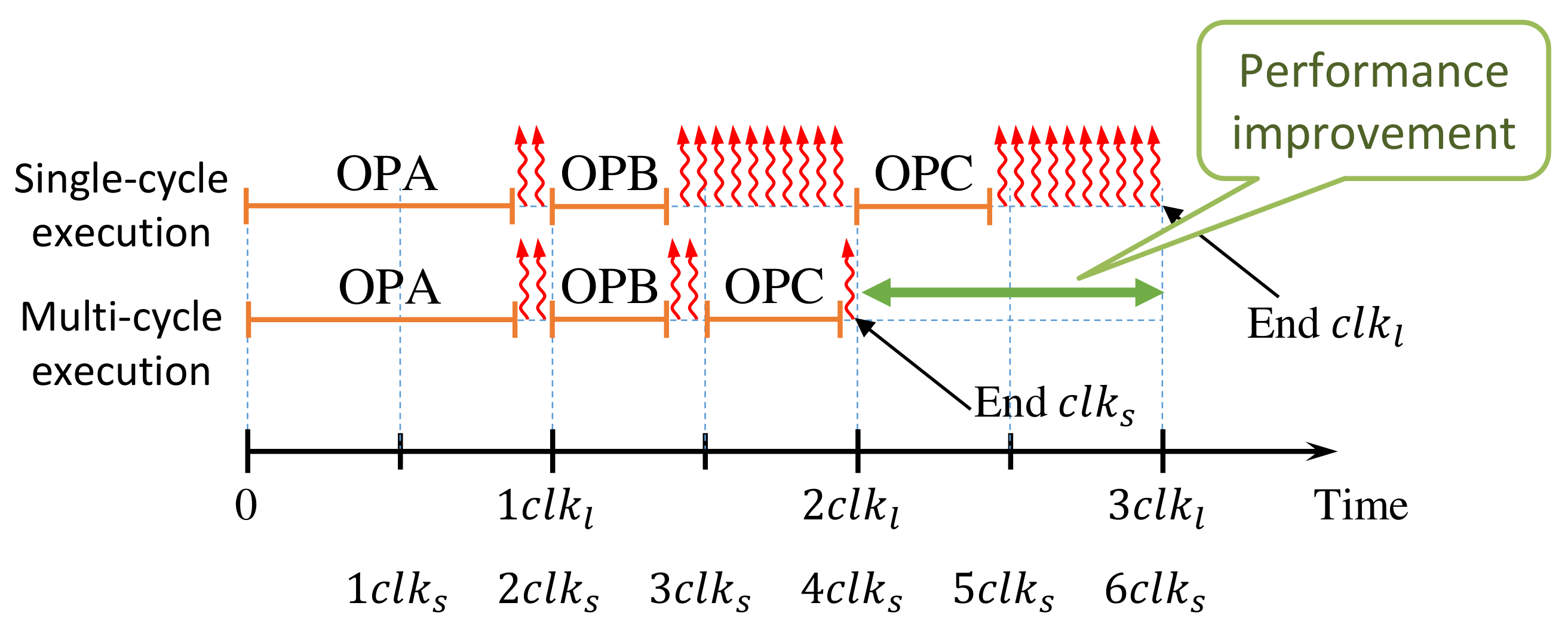
To save leakage energy, it is important to reduce the time a circuit is powered on but idle, i.e., the time a circuit is performing no operation. For this purpose, the timing slack under all operation conditions has to be trimmed. This is a very challenging task, in particular for functional units, which are fundamental components of data paths. In functional units, different operations have different timing criticalities and slacks. For instance, in an ALU, some operations need only a fraction of a clock cycle (e.g., logic operations), whereas others require a full clock cycle (e.g., addition operation with operands of long data type). Consequently, whenever an operation of the first category executed energy is “wasted” due to leakage, as the clock period is defined according to the slowest operation. Instead, it is much more efficient to execute operations of the second category at multiple cycles, which reduces the overall idle time of the functional unit, as conceptualized in Figure 6.
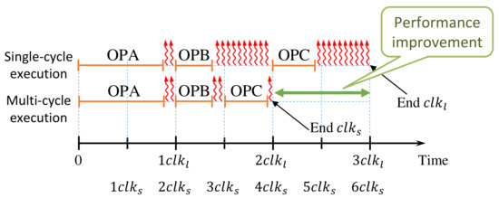
Figure 6.
Conceptual illustration of the impact of a short clock period () and multi-cycle operations (e.g., OPA) on runtime and “wasted” leakage. Leakage is illustrated by  .
.
 .
.
Additionally, when an instruction is being executed by a functional unit, some parts of the functional unit are idle as they are not exercised by the executing instruction. To tackle this issue and improve the overall energy efficiency and reliability, we revisit the structure of the functional unit by partitioning it into multiple smaller and simpler units, to enable fine-grain power gating of unexercised functional units. If a particular functional unit is not utilized by a long sequence of instruction stream, it can safely be power-gated to save leakage energy, as shown in Figure 7. Proper clustering of the instructions into several smaller functional units allows maximizing the power-down intervals of multiple functional units, and hence reducing the leakage energy. At the same time, simplifying the functional unit can reduce timing uncertainties and improve a reliable operation of NTC processors under process and runtime variations.

Figure 7.
Conceptual illustration of the impact of partitioning on a functional unit executing OPA instruction, and its impact on “wasted” leakage. Leakage is illustrated by  . (a) Executing instruction OPA on original functional unit and the associated leakage dissipation by unexercised components. (b) Executing instruction OPA on the partitioned functional unit and power-gating of smaller units.
 . (a) Executing instruction OPA on original functional unit and the associated leakage dissipation by unexercised components. (b) Executing instruction OPA on the partitioned functional unit and power-gating of smaller units.
Leakage and dynamic energy are comparable in the NTV region. Therefore, it is crucial to control the amount of leakage power to leverage the benefits of the NTC. This section presents cross-layer methodologies to optimize energy efficiency, performance, and reliability of NTC functional units based on reducing the idle time.
The leakage power can be reduced by reducing the idle time of a circuit. A circuit may become idle within a clock cycle, for example, when it has extra timing slack, or over consecutive clock cycles. The former may be avoided by modifying the circuit design to reduce the timing slack for all conditions, and the latter can be avoided by power-gating the circuit when possible.
The timing-slack minimization can be done by circuit synthesis techniques, which are tailored for NTC circuits [75,98]. However, these approaches are not much efficient when dealing with functional units (e.g., adders, multipliers, or complete ALUs) as the timing slacks of the instructions may be widely different [106]. For example, a simple instruction such as a Bitwise-AND only needs a fraction of the clock cycle, whereas an ADD instruction could use a large portion of the clock cycle. As the delays of these instructions are intrinsically different, the NTC synthesis techniques are not able to effectively balance the delay of these two instructions. We propose to execute the slow instructions in multiple cycles and the fast instructions in a single clock cycle (instruction multi-cycling) as the solution to this problem [106]. Applying other optimization techniques such as opportunistic circuit synthesis, instruction replacement, and data type manipulation can further improve the effectiveness of the proposed method. The proposed instruction multi-cycling method is described in Section 4.2, the developed methodology is explained in Section 5.1, and its experimental results are discussed in Section 5.4.
In a real-world scenario, an executed application may utilize only a fraction of the instructions implemented inside a functional unit. This means that during the execution of such applications, those gates of the functional unit that are exclusively used by the non-exercised instructions of the functional unit are not utilized. The leakage power from these gates contributes to the dissipated energy of the system. On the other hand, it is not feasible to power off the entire functional unit because any of the instructions can be called at a time. We propose to address this by redesigning the entire functional unit to allow power-gating [107]. In this approach, a large functional unit such as an ALU is partitioned into several smaller functional units such that each unit can be power-gated separately (functional unit partitioning). For this purpose, the instructions need to be clustered properly into different groups. A number of parameters such as the instruction utilization pattern, the temporal distance between the instructions inside an application instruction stream, and intrinsic similarity between the instructions need to be considered for a proper clustering. Accordingly, the instruction stream of various applications has to be analyzed to extract the required information for clustering [107]. The proposed functional unit partitioning method is described in Section 4.3, the developed methodology is explained in Section 5.1, and its experimental results are discussed in Section 5.5.
4.2. Instruction Multi-Cycling
This scheme consists of four main ideas to fully enable the potential of NTC:
- We classify the instructions into slow (with little timing slack) and fast (with large timing slack), based on the time required to execute the instructions. The slow instructions are executed in multiple clock cycles, to reduce the leakage power while executing fast instructions within one clock cycle.
- Contrary to the super-threshold regime, we use relaxed timing constraints for the synthesis of functional units in the NTV region. While this increases the delay of the most critical path, it avoids that all instructions have similar delays and belong to the same category. By that means, the scheme of point 1 is much more efficient.
- Finally, the clock period is not only set according to points 1 and 2 but also by considering the sensitivity of the functional unit to variations. As a result, it is possible to co-optimize energy, performance, and reliability.
- In order to reduce the number of “slow” multi-cycle operations, we propose to employ instruction- and compiler-level optimization approaches to replace some of these instructions in the code with fast single-cycle instructions, which further improves energy and performance.
4.2.1. Energy Improvement through Instruction Multi-Cycling
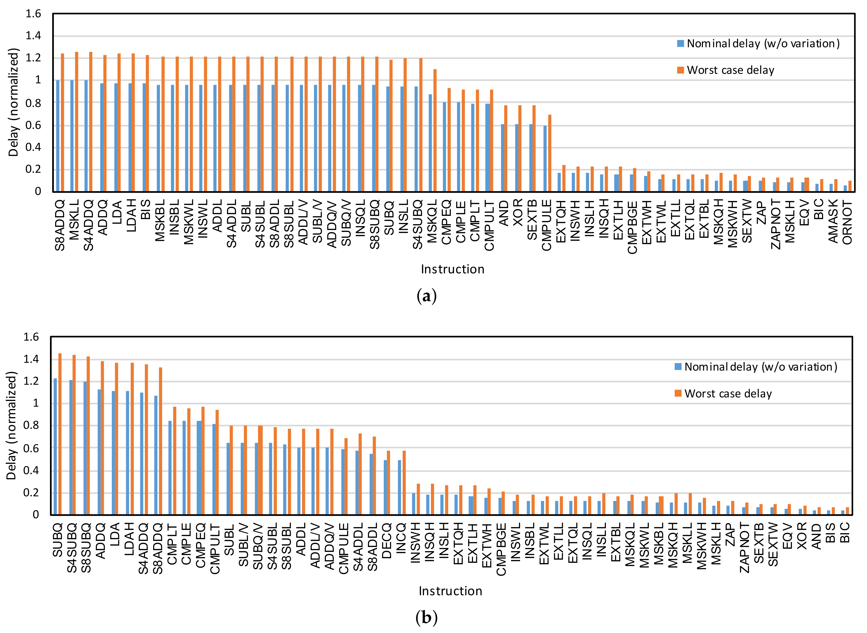
The propagation delay of functional units is typically dependent on input vectors. For example, in an ALU, the instructions can be categorized into slow instruction and fast instructions and the delay gap between fast and slow instructions might be significant. The logical operations such as inversion can be executed very fast while the execution of arithmetic operations such as addition and subtract requires more time. Figure 8a shows the normalized delay of various instructions of an ALU at 0.5 V (according to the simulation setup presented in Section 5). The synthesis tool balances as many paths as possible to optimize the energy given the timing constraints. In this case, 26 instructions are balanced to be critical or near-critical in terms of timing (slow instructions); however, the rest of the instructions require less time for completion (fast instructions).
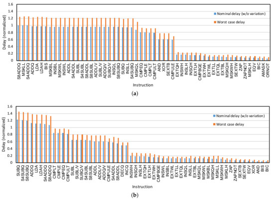
Figure 8.
Nominal instruction delay without considering the impact of process variation and worst case instruction delay (considering process variation) are depicted for the instructions of an Arithmetic Logic Unit (ALU) synthesized with (a) typical timing constraint (Tight ALU) and (b) loose timing constraints (Loose ALU). The worst case delay is extracted by statistical static timing analysis (SSTA) as of the instruction delay. All the numbers are normalized to the maximum nominal delay of the Tight ALU, which is the nominal delay of S8ADDQ in (a). The depicted figures are obtained for a 64-bit ALU based on the simulation setup explained in Section 5.3 at V.
In a traditional design approach, the delay of the unit is determined by the delay of the slowest instruction. Therefore, during the execution of the fast instructions, the ALU finishes the execution early and leaks for the rest of the clock cycle. The “dissipated” leakage energy is more important in the NTC because (1) the leakage energy is significant and constitutes a significant portion of the total energy, (2) the delay gap between the fast instructions and the slow instructions is even more pronounced due to the impact of process variation. As shown in Figure 8a, the amount of variation induced delay (the difference between the nominal delay and the worst-case delay) is larger for the slow instructions, which significantly increase the delay gap between the slow and fast instructions in the near-threshold regime.
Our proposed idea is to reduce the leakage energy by using a shorter clock period and execute the slow instructions in multiple cycles. For example, in the presented ALU in Figure 8a, it is possible to reduce the clock period to half of the delay of the slowest instruction and execute the slow instructions (from S8ADDQ to CMPULE-totally 35 instructions) in two cycles and the rest of the instructions in one cycle. Therefore, once a fast instruction is executed the amount of the wasted leakage energy would be much smaller compared to the traditional approach. This would also improve performance because fast instructions require less time for execution.
For the execution of the slow instructions, which may require more than one cycle, there is no need to insert any flip-flops or latches into the circuit. During the execution of such instructions, the inputs of the circuit are kept unchanged in order to allow the circuit to complete the execution of the slow instructions in more than one clock cycle. Therefore, it is necessary to make some modifications in the microprocessor, as discussed in Section 5.4.5.
We propose a set of cross-layer techniques from logic synthesis to compiler level in order to leverage the maximum benefits from the proposed method by moving more executed instructions to the “fast” category.
4.2.2. Logic Synthesis for NTV Region
In order to show the impact of the logic synthesis on the ALU, we synthesized the same ALU with two different strategies. First, the ALU is synthesized with tight timing and area constraints, which is the default strategy in the super-threshold region. From now on, we refer to this synthesized ALU as Tight ALU. As the results depicted in Figure 8a show, the synthesis tool balanced the delay of many instructions (mostly arithmetic instructions) to maximize the energy efficiency and performance. However, there are still many instructions (mostly logic instructions), which are too short to be balanced similar to the slow instructions. Furthermore, there is a sharp transition from the delay of slow instructions to the fast instructions.
Then, the same ALU is synthesized with loose timing and area constraints (Loose ALU). The results of this synthesis are shown in Figure 8b. Since the synthesis tool is not under tight constraints, the delays of the slow instructions are larger compared to the Tight ALU, and there is a smooth transition from the delay of the slow instructions to the fast instructions.
In summary, the synthesis results based on the simulation setup presented in Section 5.3, show that the performance of the Tight ALU is better than the Loose ALU by 13% considering the variations; however, due to the wide spectrum of the delays of the instructions in the Loose ALU, there are more opportunities for improving the ALU with the envisioned multi-cycling technique. The reason is that fewer instructions are critical in terms of timing and by cleverly choosing the clock period we can gain in terms of energy and performance, as shown later in Section 5.
4.2.3. High-Level Optimization Techniques
From the above discussion, we observe that some ALU instructions are slower with longer execution time, while other instructions are faster with shorter execution time. Therefore, the aim is to exploit high-level optimization techniques such as data type conversion and instruction replacement to replace slower instructions of an application by fast ones wherever possible, so that the overall energy demand will be reduced further. Since the slower instructions are executed in multiple clock cycles, replacing them with faster instruction can also improve the performance by reducing the Cycle Per Instruction of the applications.
Data type conversion: The selection of data types for variables has a huge impact on the instruction binary generated by the compiler. The data types such as short (1-byte), char (2-byte), int (4-byte) and long (8-byte) not only specify the storage space size of variables but also the type of operation on the variables (e.g., 64-bit arithmetic such as ADDQ vs. 32-bit arithmetic such as ADDL). This affects the occurrence rate of slower and faster instructions within an application. Hence, in addition to memory optimization, a clever data type selection will help to save energy by using fast instructions (e.g., ADDL in Figure 8b) instead of the slow ones (e.g., ADDQ in Figure 8b).
Instruction replacement: Many applications such as sorting and matrix multiplication algorithms spend most of the execution time in loops. Hence, simple instructions such as increasing loop counters and array indexes significantly contribute to the overall instruction count. If such instructions are not assigned appropriate data type and operation, they can impose significant performance and energy overhead. For instance, since modern ALUs have a dedicated increment/decrement circuitry, the usage of increment/decrement instructions plays a vital role in improving the performance and energy efficiency by reducing the number of slower instructions. This and other instruction replacements (e.g., shift instead of multiplication) can be achieved either by the programmer or using different compiler optimization techniques.
4.3. Functional Unit Partitioning
Fine-grained power-gating has been known as an effective solution for reducing the leakage power consumption of a system by cutting the supply lines of the idle components [105]. However, it is costly to power-on and power-gate the components in terms of execution time as each power-gating cycle mandates a minimum time between power-on and power-off cycles. Once a component is put to sleep, its functionality cannot be used. Therefore, the components should be carefully tailored towards power-gating.
One opportunity for power-gating of the components is to determine the unused parts of a circuit based on the running application and power-gate those specific parts instead of the entire component. For ALUs executing several instructions, unused parts of the ALU corresponding to the instructions not executed for a long time could be safely power-gated. Figure 9 presents the usage frequency of a 64-bit ALU (for Alpha ISA). As shown in the figure, there are orders of magnitude differences between the usage frequency of a highly used instruction such as LDA and a rarely used instruction such as ZAP. If both of the mentioned instructions are implemented in a single ALU, the circuitry for ZAP is leaking most of the time while being at an idle state. In other words, the gates that are implemented exclusively for the rarely used instructions are in the idle state most of the time and are contributing to the total leakage of the ALU.

Figure 9.
Instruction usage frequency in a 64-bit ALU for gzip workload. There are orders of magnitude differences between utilization frequency of “highly used instructions” on the left and “rarely used instructions” on the right. The depicted figure is obtained by executing SPEC2000 workload “gzip” using the gem5 simulator, as explained in Section 5.3.
Our proposed solution is to partition a functional unit like an ALU into multiple smaller ALUs. This allows us to power-gate some of the ALUs based on the utilization of their instructions by turning off the ALUs that are not currently being used. The original ALU could be partitioned based on different parameters such as the instruction utilization frequency, instruction similarity, and instruction temporal proximity.
In summary, this scheme synergistically exploits NTC in conjunction with a fine-grained power-gating of functional units to enable energy-efficient operation of devices designed for IoT applications. A hierarchical clustering algorithm groups the instructions into smaller functional units by considering the frequent instruction sequences, obtained by application profiling, in order to maximize power-gating intervals. Accordingly,
- We characterize the instruction flow of representative workloads and analyze the instruction stream in order to obtain instructions’ utilization frequency and temporal distance.
- The instructions are then partitioned into several groups according to the metrics extracted from the instruction stream analysis as well as the inherent similarity of the instruction.
- Each set of instructions residing in the same partition will be implemented by a dedicated functional unit, and they form a complete functional unit altogether.
- To reduce the leakage power, only the functional unit corresponding to the running instruction partition is activated while other units are power-gated.
4.3.1. Instruction Pattern Analysis
A careful analysis of the instruction patterns on a set of representative workloads provides information regarding the ALU partitioning. For this purpose, we first simulate the execution of a set of representative workloads by an architectural simulation tool as explained in Section 5, and then based on the extracted instruction streams the utilization frequency and the temporal distance of different instructions are extracted.
Instruction utilization frequency: The instruction utilization frequencies presented in Figure 9 show a significant difference in utilization among the instructions. The instruction utilization frequency has an inverse relation with the power-gating feasibility for the ALUs associated with the instructions. For example, the ALUs that contain instructions ADDQ and BIS are less likely to be power-gated because these instructions appear in the instruction buffer on average every 10 cycles. However, it is more likely to power-gate the ALUs implementing the rarely used instructions on the right side of Figure 9 such as S8ADDL.
The utilization frequency of an instruction can be simply defined as the number of cycles in which the instruction is executed divided by total cycles. For a given instruction stream S, which is a sequence containing instructions, we can define the frequency of instruction A as:
where is the i-th element (instruction) of S. If an instruction is used rarely, it can be easily grouped into any existing ALUs. However, we need to be more cautious in grouping frequently used instruction because the grouping strategy might improve or deteriorate the power-gating capability of the ALUs. Based on this analysis, we can define the frequency distance metric between two instructions A and B as the geometric mean:
Such definition facilitates the partitioning of rarely used instructions into a single ALU.
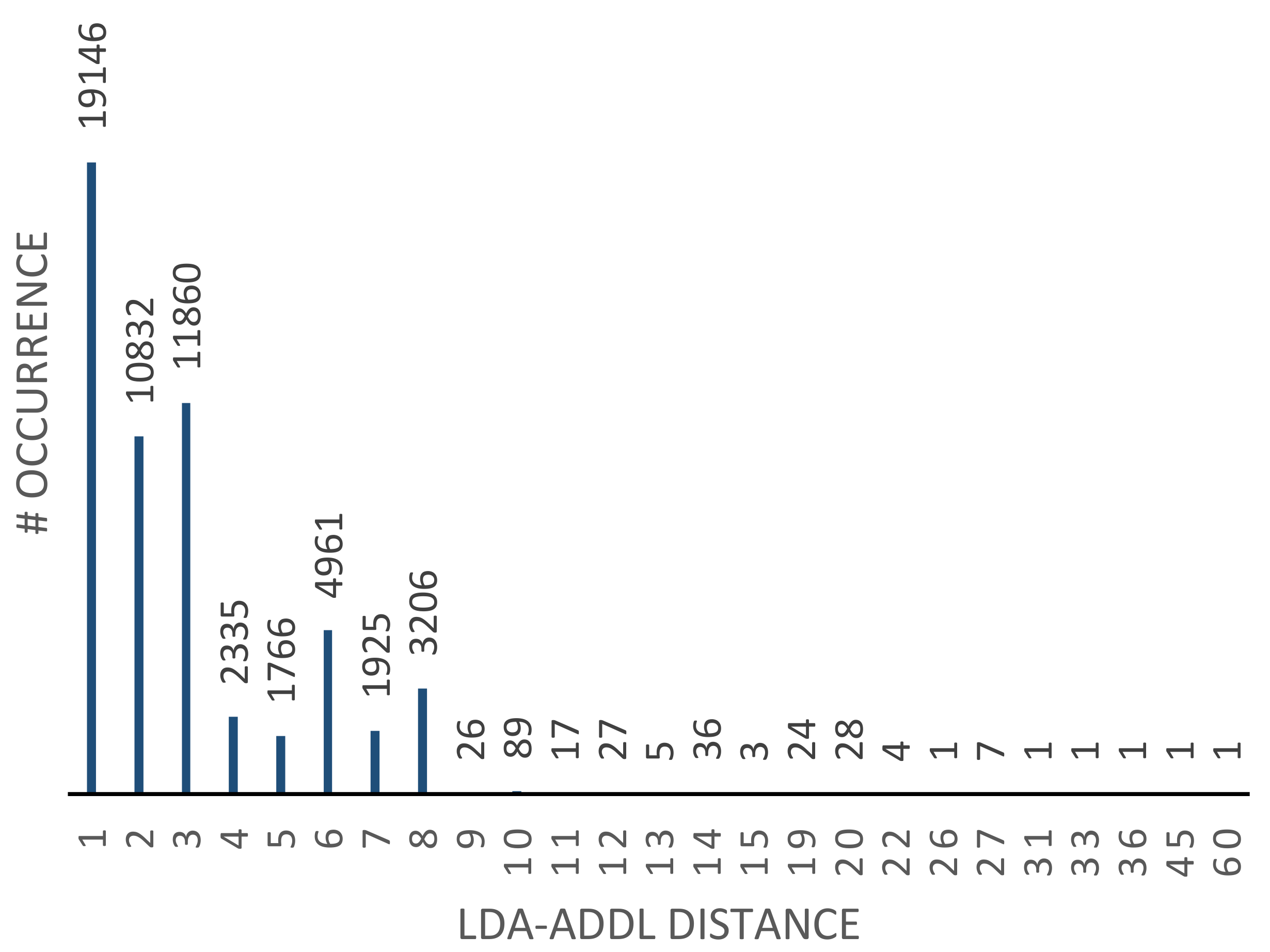
Instruction temporal distance: Some instructions are more likely to appear next to each other in an application. For example, from “bzip2” workload, we observed that ADDL appears after LDA on average every 2.97 instructions (see Figure 10). In these cases, it could be beneficial to group these neighboring instructions inside one ALU in order to improve the power-gating interval for other ALUs.
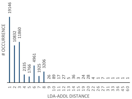
Figure 10.
The temporal distance between LDA and ADDL instructions in “bzip2” workload (simulation for 2 million cycles). There are 19,146 cases in which the ADDL instruction appeared right after LDA. The average distance is 2.97. The results are obtained using gem5 simulator as explained in Section 5.3.
The temporal distance between two instructions A and B can be extracted based on the number of cycles between any occurrences of A and B. For example, according to the results presented in Figure 10, there are 19146 LDA instructions that are directly followed by an ADDL instruction, and there are 11860 LDA instructions that are followed by an ADDL instruction after three cycles. Based on the workload analysis, a distribution is extracted for every instruction pair A-B, which explains the percentage of the A-B pairs that are far from each other by k cycles. The Survival Function (SF) (defined as of a distribution) of these temporal distance distributions is useful in the clustering problem definition in Section 4.3.2.
We define a temporal distance set which contains the indexes of consequent instructions A and B and their corresponding distances :
Accordingly, the Probability Mass Function (PMF) based on distance k is calculated as:
The extracted PMF is then used to find the SF as follows:
In a fictitious scenario where only instructions A and B exist, and they are divided into two ALUs, the SF can explain the power-gating possibility. In this case, if the minimum number of cycles required to perform a power-gating (power-gating threshold) is , then obtains the power-gating probability. Therefore,
can be used as the temporal distance metric between two instructions A and B.
Instruction similarity: Many instructions share some gates in ALU mostly due to their similarity. For example, an ALU could have different addition and subtraction instructions, which are inherently similar. As a result, these instructions share a large portion of gates in the synthesized netlist. Therefore, implementing these instructions in separate ALUs would impose redundant structures leading to undesirable leakage and area overhead. Therefore, it is preferable to group such instructions into one ALU to reduce the associated overheads.
We introduce a dissimilarity metric defined as the structural dissimilarity between instructions (). For example, as both addition instructions implement similar functionality. However, as the corresponding instructions implement two completely different logic structures. The dissimilarity values are assigned based on the knowledge we have about the logic implementation of different instructions.
Some of the above parameters may lead to contradictory grouping of instructions into ALUs. For example, instructions S8ADDL and ADDL should be grouped into one ALU because of inherent similarity; however, according to their utilization frequencies they should be placed into different ALUs to allow power-gating. In the next section, we define a formal clustering problem considering the aforementioned parameters and solve it to find the best instruction grouping strategy.
4.3.2. Instruction Clustering Problem Definition
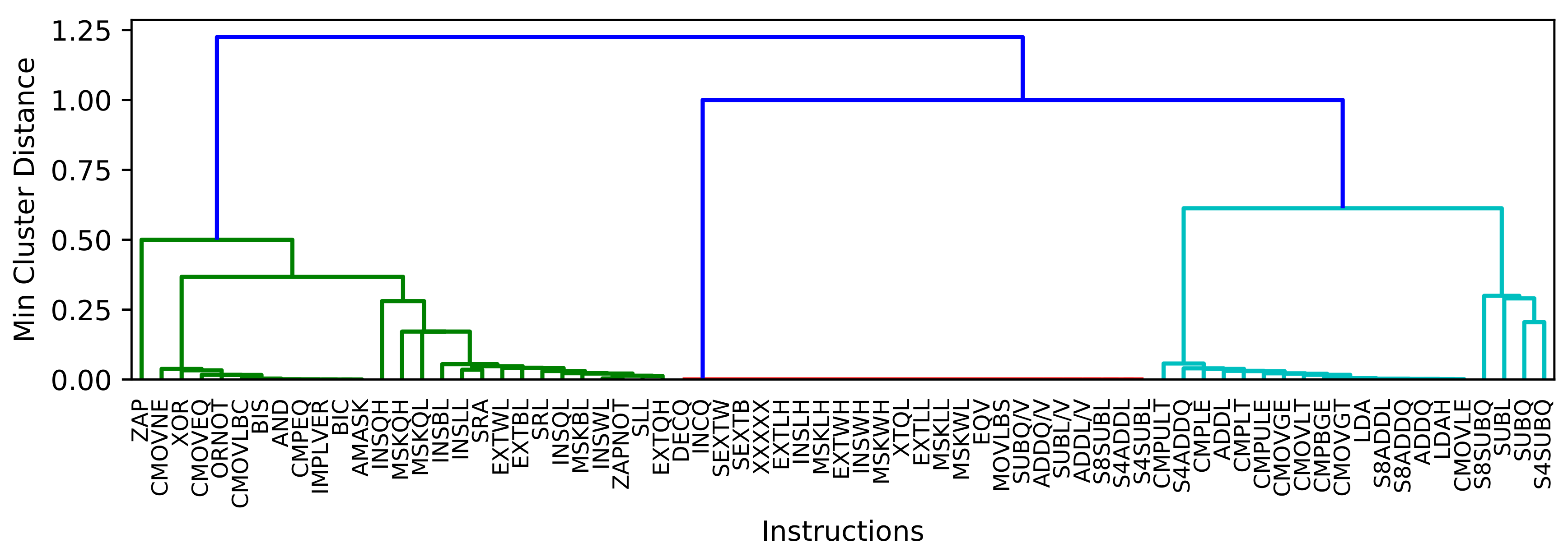
The problem of partitioning a large ALU into smaller ALUs can be defined as a clustering problem, in which the distance between the instructions is explained by temporal proximity, utilization frequency, and similarity of instructions. The goal of such clustering algorithm is to maximize the distance between ALUs while minimizing the distance between instructions of each ALU. This allows us to increase the overall power-gating likelihood of ALUs, which leads to lower leakage and better energy efficiency.
For this purpose we apply the Agglomerative Hierarchical Clustering (AHC) algorithm [108] to cluster the instructions into several groups, each group implemented in one ALU. AHC is suitable for our problem because we can provide pairwise distances between each and every two instructions.
We create the pairwise distance matrix needed for the AHC algorithm based on the frequency distance metric (), temporal distance metric (), and structural similarity () introduced in the previous section. Finally, the elements of the pairwise distance matrix () are obtained as (Cartesian distance on a 3D space):
Here, are coefficients to scale all the metrics into the same scale.
We consider the single-linkage clustering method on the AHC. In a single-linkage method, the linkage function , which is the distance between two clusters X and Y, is defined as the minimum distance between every two members of the clusters:
Therefore, maximizing the distance between clusters X and Y will allow the maximum power gating possibility of the corresponding ALU implementations and improves the energy efficiency.
4.3.3. Fine-Grained Power-Gating Prediction
Once the inactive phase for a component is detected at architecture-level, the component can be power-gated by asserting a sleep signal on the header/footer sleep transistors. Although the power-gating can effectively reduce the wasted leakage energy, it has to be done when the functional unit is not utilized for a minimum number of cycles () to break-even the associated overheads. This value is estimated to be around 10 cycles for a typical technology [105,109].
The inactive phase of a functional unit can be predicted based on several techniques at runtime. In order to determine the inactive interval of each functional unit and decide whether to power gate it or not, it is possible to monitor the instruction buffer for a number of upcoming instructions while considering the branch prediction buffer. However, the power-gating signal for a given functional unit can be mispredicted due to branch misprediction. As a result of misprediction, the entire pipeline may be needed to be flushed to reload the correct instructions. This provides some time to properly power up the required functional units without imposing much overhead due to pipeline stall. It is worth mentioning that sub-threshold and near-threshold processors typically have a deeper pipeline to benefit in terms of performance and energy efficiency [110]. In such processors, there is enough time for functional unit power up after misprediction due to deeper pipeline design.
In Out of Order (OoO) processors, the order of execution of the instructions can slightly change at runtime in order to avoid stalls in the pipeline. As a result, predicting the idle time of the functional unit partitions is not straightforward. The proposed functional unit partitioning method can be used whenever such prediction is possible; however, without good prediction methods, the proposed method may not bring significant improvement to the design. In the presented experimental results in Section 5.5, we evaluated the results with the assumption of in-order execution of the instructions. Further development and application of the proposed functional unit partitioning method to OoO designs is not presented in this paper.
5. Results and Discussion
This section presents the methodology and simulation setup for the proposed data path optimization approaches. We evaluate the effectiveness of the proposed approaches by applying them to an ALU.
5.1. Implementation Flow
5.1.1. Input Vector Dependent Timing and Power Analysis
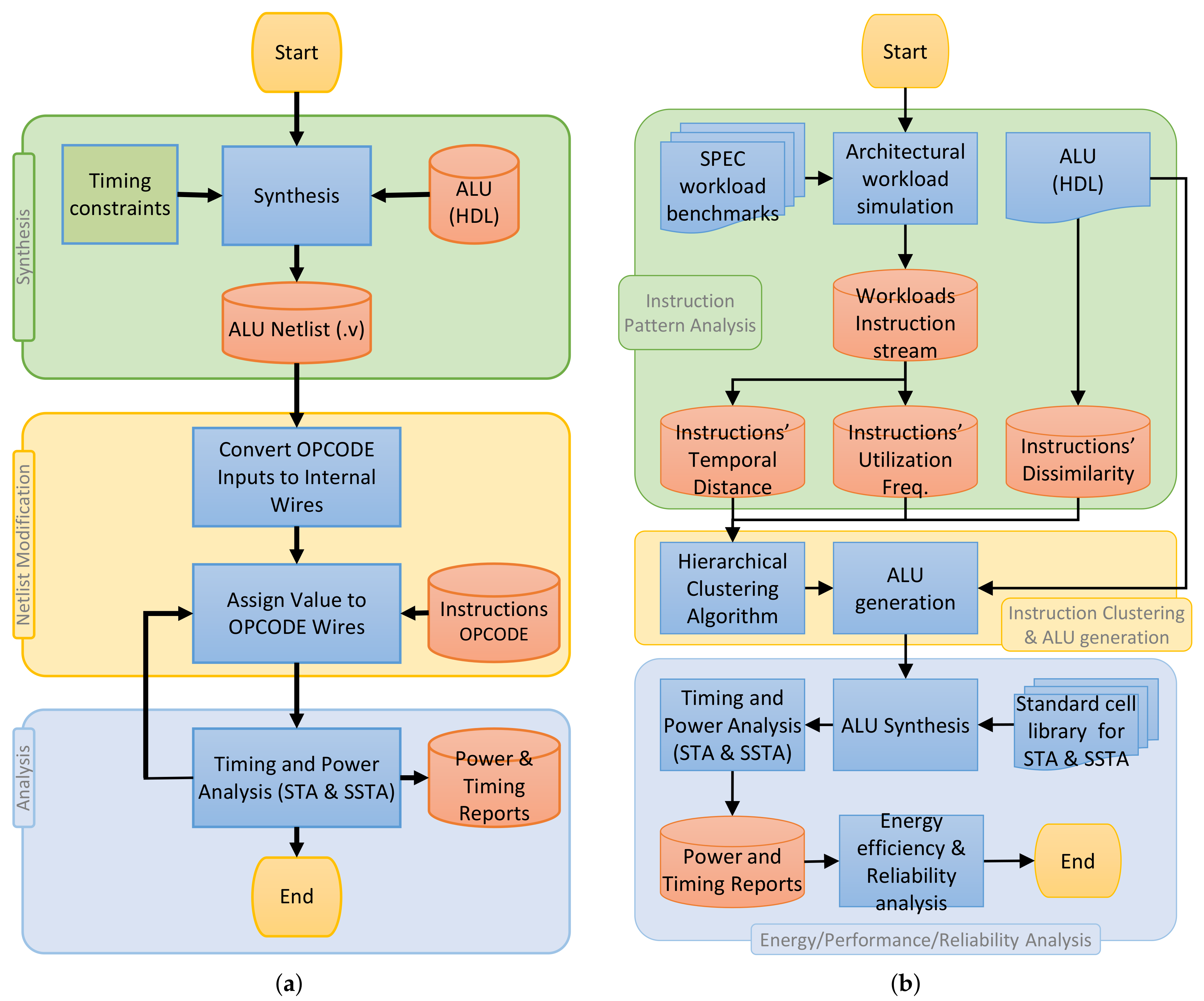
As explained in Section 4.2, the time and power required by a functional unit to complete an operation execution is different from one instruction to another. Here, we use the flow illustrated in Figure 11a to extract the detailed timing and power information for each instruction. Therefore, for an ALU as a case study the following steps are performed:
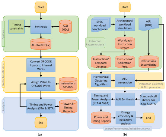
Figure 11.
Implementation flows of (a) instruction multi-cycling, (b) functional unit partitioning applied to an ALU. (a) Implemented flow for obtaining the timing and power information of each ALU instruction, in the instruction multi-cycling approach. (b) Implemented flow of the proposed functional unit partitioning for ALU optimization.
- Synthesis: The synthesis step of Figure 11a is executed with timing constraints to obtain the gate level netlist of the synthesized ALU.
- Netlist modification: The synthesized netlists of the ALUs are modified such that the OPCODE input signals that determine the instruction to be executed are changed to internal wires. For each instruction, the OPCODE signals are assigned to associated values inside the Verilog netlist. This will effectively deactivate the rest of the instruction paths in the ALU and force the STA tool to evaluate only the paths associated with the execution of the given instruction. This is because the rest of the paths (which belong to other instructions) are deactivated, and any change in the output pins of the ALU is only due to the paths belonging to the given instruction.
- Timing and power analysis: The timing and power analyses are performed on the modified netlists, and the delay of the instructions considering the variation as well as the dynamic power and the leakage power for each instruction are extracted.
The change in the leakage power from one instruction to another is negligible because even the inactive gates that are not part of the propagation paths are leaking. However, if the execution time is different from one instruction to another, the amount of the leakage energy would be different proportionally. The dynamic energy for each instruction is also calculated based on the dynamic power value.
5.1.2. Functional Unit Partitioning Flow
Figure 11b shows the overall flow of the proposed functional unit partitioning method applied to an ALU. The flow consists of three distinct steps:
- Instruction Pattern Analysis: In this step, the instruction stream extracted from running representative workloads are analyzed to extract instruction temporal distance and utilization frequency. Instruction dissimilarity is also defined based on the field knowledge about the implementation of logic units.
- Instruction Clustering and ALU generation: With the help of the information collected from the previous step, instructions are grouped into n clusters, and each cluster is implemented as a new ALU. Moreover, all the partitioned ALUs are combined with a circuit for multiplexing their outputs to form a union ALU, as shown in Figure 7b.
- Energy, Performance and Reliability Analysis: The union ALU generated from the previous step is evaluated in terms of timing and performance, and finally, its reliability is evaluated when it is used instead of the original ALU.
5.2. Reliability Analysis
Various sources of delay variation, for example, process variation, aging, temperature and voltage variations, can potentially lead to timing failures. Therefore, timing failure is presented as a stochastic metric, which is dependent on the value of an additional timing margin and hence the allocated clock period. Therefore, statistical information regarding the circuit delay can be used to evaluate the reliability. Accordingly, Reliability is the probability of not having a timing failure due to variation effects.
In a functional unit such as an ALU, the Failure Probability of a circuit caused by timing issues can be modeled as a function of the allowed time for instruction execution T, based on the delay distributions of the instructions:
where is the Cumulative Distribution Function (CDF) of delay of instruction INST. Accordingly, the Failure Probability is obtained as:
There is a trade-off between reliability and performance as explained in the above equation. A larger clock period (T) results in higher reliability and lower failure probability at the cost of speed.
In a multi-cycling scenario, the allowed time for instruction execution T is dependent on the number of cycles allocated by each instruction. For a single-cycle instruction T is equal to the clock period ; however, a two-cycle instruction is allowed to be executed for . Therefore, Equation (14) is modified as follows:
In the above equation, is the number of cycles allocated for instruction INST obtained based on the distribution of the instruction delays:
is the instruction delay considering the variation, i.e., a point in the tail of the delay distribution referring to very low failure probability. Please note that slow instructions have large logic depth, i.e., there are many gates in the critical paths of these instructions. According to the Central Limit Theorem [111], the delay distribution of such instructions is approximately normal (Gaussian). In such case, we can use parameters such as the mean () and standard deviation () of instruction delay to approximate its CDF function. Therefore, we may choose of the instruction delay as , which corresponds to less than 0.135% failure probability.
We perform SSTA to evaluate the impact of process variation [112] on the timing of the circuit. The SSTA tool reads variation information from the variation library (see [71]) containing variation information at the cell-level. The SSTA extracts accurate delay distribution for each instruction of the ALU represented by their CDF (i.e., ). Based on these distribution functions and Equation (16), we extract the reliability of the ALU.
5.3. Simulation Setup
The proposed approaches are applied to a 64-bit ALU, namely the ALU of the Illinois Verilog Model (IVM) [113], which is a Verilog model for the Alpha 21264 core. The selected ALU implements 64-bit RISC Instruction Set Architecture of Alpha processor. For this purpose, we synthesize the HDL from the IVM ALU with loose and tight timing constraints and characterize it for the NTC by an SSTA to extract the power and delay of each instruction as well as the reliability as explained in Section 5.1. The synthesis is done using the Synopsys Design Compiler [114]. Statistical static timing analysis (SSTA) is done using a Cadence Encounter Timing System [115], which is able to perform SSTA using statistical CCS or ECSM standard cell library models [116].
In order to prepare such statistical standard cell libraries for timing and power analysis, the cells from selected libraries [117,118] from 32 nm down to 10 nm are re-characterized using the Cadence Virtuoso Variety [119] and the cells that are not suitable for NTC are excluded from the library [33]. The Variety tool characterizes the cells considering the process variation and all the power and delay values are stored in the generated standard cell libraries. The process of library characterization can be time consuming. However, this is only done once and the obtained libraries can be used in different projects.
The SSTA performed by this method is applicable to the NTV region, because it can consider a skewed delay model for the cells. Each SSTA timing analysis run takes more execution time compared to a simpler STA run, which is typically done at nominal supply voltage ranges. Nevertheless, it is still much faster compared to a Monte-Carlo-based SSTA. The same method is applied to synthesize and analyze the partitioned ALUs generated by the functional unit partitioning method.
Additionally, we extract the instruction stream for SPEC2000 benchmark workloads using a gem5 architectural simulator [120]. This is done by executing the workloads using gem5, fast forwarding to the start of the executed workloads, and collecting all the executed instructions and the provided operands. The result of the architectural simulation is used to evaluate the impact of the proposed instruction multi-cycling approach and to perform instruction pattern analysis and clustering in the proposed functional unit partitioning approach. The results of both approaches are compared to the baseline, which is an IVM ALU that is synthesized with conventional tight timing constraints.
5.4. ALU Multi-Cycling Results
5.4.1. Multi-Cycling Improvement
By reducing the clock period below the delay of the slowest instruction, some instructions need to be executed in multiple clock cycles. The number of the required clock cycles can be calculated from Equation (17). The delay of the slowest instruction is 146 ns; hence, the minimum clock period for running all instructions in one cycle is also 146 ns.
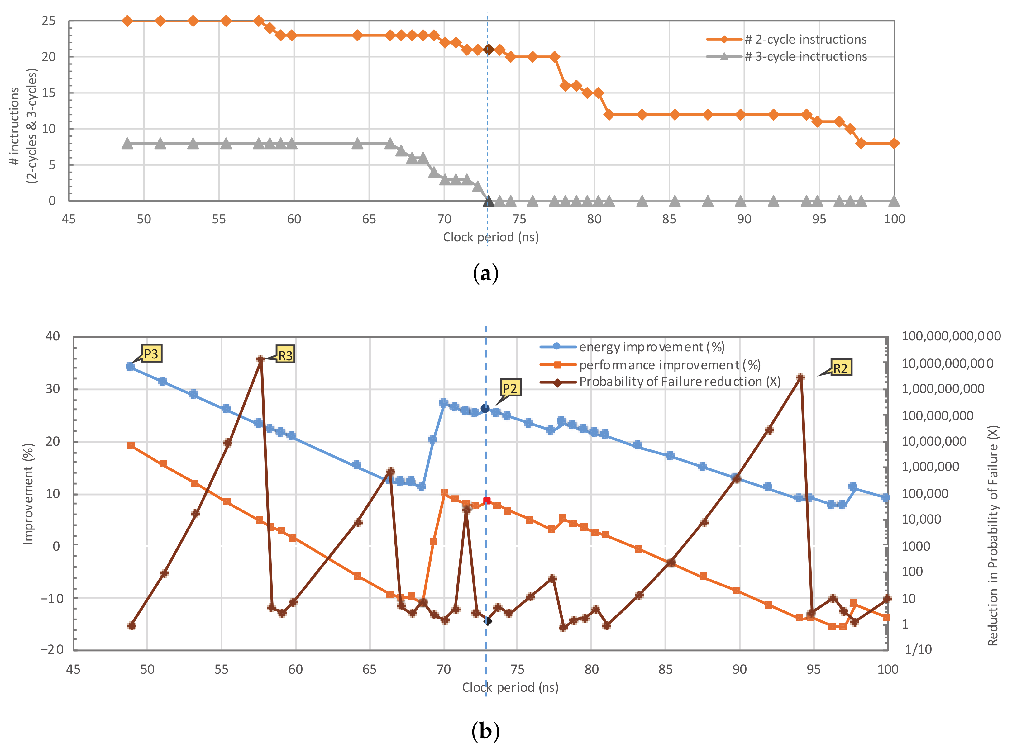
We changed the clock period of the Loose ALU and extracted the instructions, which should be executed in multiple cycles for each clock period. Here, the clock period is swept from 49 ns (one-third of the delay of the most critical instruction) to 100 ns to explain the impact of clock period on the circuit characteristics. As shown in Figure 12a, some instructions need to be executed in three cycles when the clock period is below 73 ns (which is half the delay of the most critical instruction—marked by a vertical dashed line in the figure).
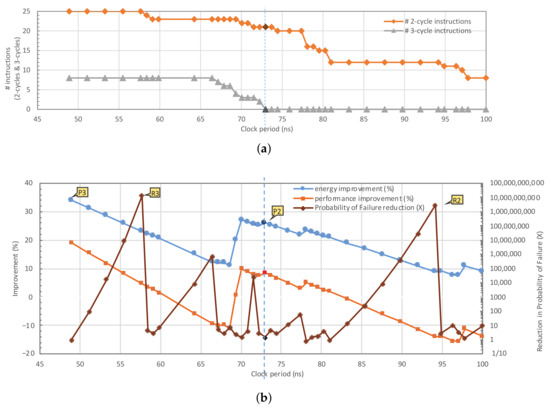
Figure 12.
Modifying the clock period of the ALU changes the set of 2-cycle and 3-cycle instructions, which impacts the energy, performance and reliability improvements significantly. The results are extracted for Loose ALU + INC/DEC running workload “equake” at V (for other workloads the improvement plots show a similar trend). The improvement values are relative to the Tight ALU. Four Pareto points are marked on the graph: P2 (R2) provides the best energy and performance (best reliability) when ALU is limited to execute all instructions in two clock cycles, and P3 (R3) provides the best energy and performance (best reliability) when some instructions can be executed in three clock cycles. (a) Number of 2-cycle and 3-cycle instructions for different clock period values. (b) Energy, performance and reliability improvements for different clock period values.
The energy and performance improvement of the ALU executing workload “equake” are plotted in Figure 12b for various clock periods. The improvement numbers are calculated in comparison with the Tight ALU, which executes all instructions in one clock cycle. When the clock period is reduced, the energy and performance improvements increase because the delay slacks of the instructions are trimmed. However, when any change in the sets of 1-cycle, 2-cycle or 3-cycle instructions happens due to the clock period reduction, i.e., some 1-cycle instructions become 2-cycle instructions or some 2-cycle instructions need to be executed in three cycles, the improvements suddenly drop. The maximum energy improvement (34%) and performance improvement (19%) are achieved when the clock period is 49 ns.
5.4.2. Impact of Workload on the Improvement Ratio
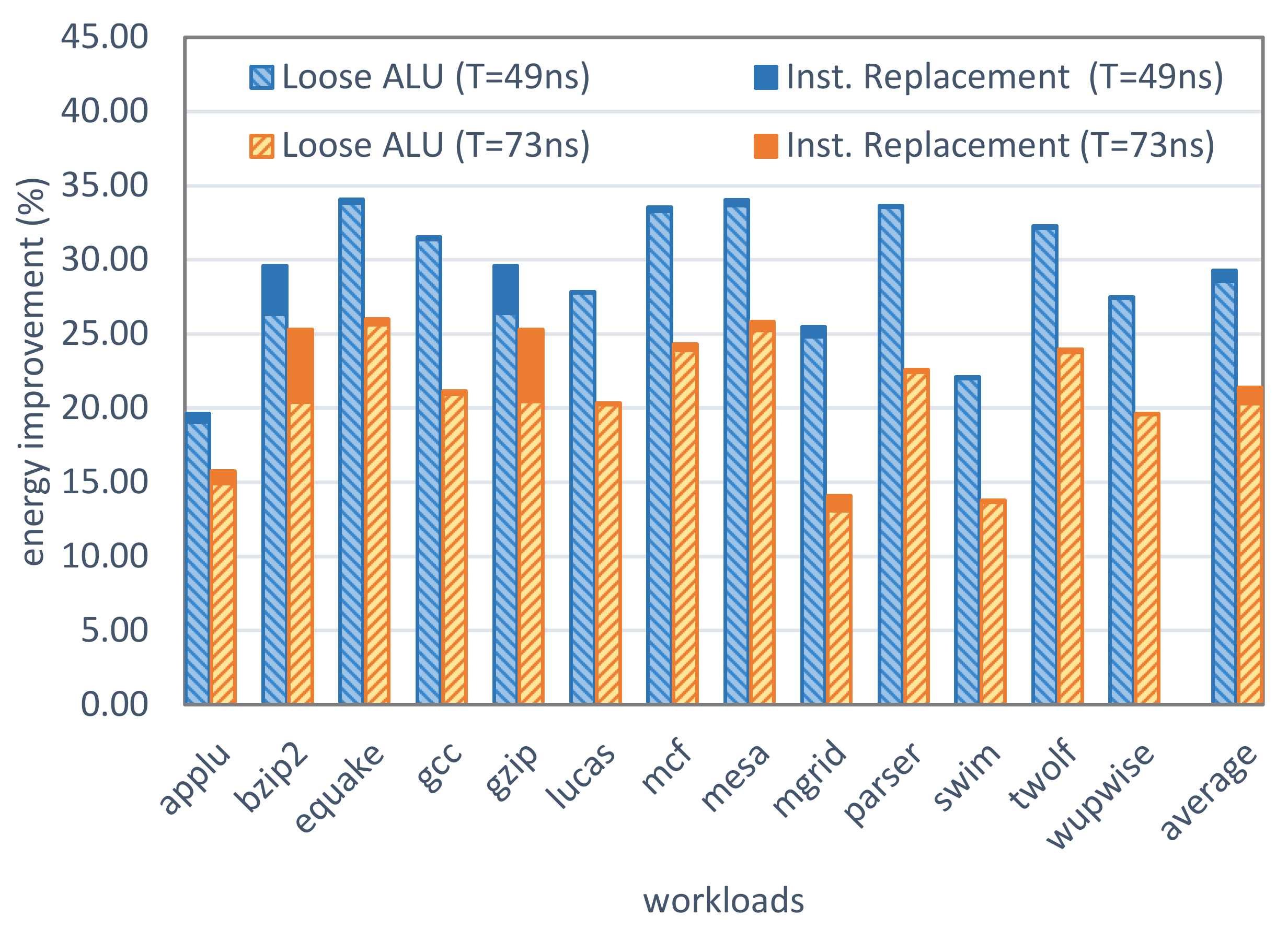
Executing a slow instruction has no performance or energy benefits because it utilizes the ALU for several clock cycles. However, executing a fast instruction, which can be executed in fewer clock cycle(s) will save some energy and improve performance. Since each workload executes a specific set of instructions, the amount of improvement is highly dependent on the profile of the instructions utilized by a workload. Workloads that frequently execute fast instructions will have better improvements using the proposed approach. We measured the amount of energy improvement for different workloads, as shown in Figure 13. The clock period is once set to 73 ns, which means all instructions are executed in at most two clock cycles, and then set to 49 ns to evaluate the results for when the instructions can occupy three clock cycles. The hatched bars in this figure show the amount of energy improvement in different workloads compared to the baseline. The improvement is smaller for workloads that frequently execute slow instructions (applu, mgrid, swim), and larger for workloads with more executions of fast instructions (equake, mesa, mcf, twolf). For example, 76% of the executed instructions in “applu” are among the eight slowest instructions (addq, lda, ldah, s4addq, s4subq, s8addq, s8subq, subq, as depicted in Figure 8b). However, this is only 45% for workload “equake”. The average energy improvement and the performance improvement over all workloads are 20.8% and 1.7%, respectively.
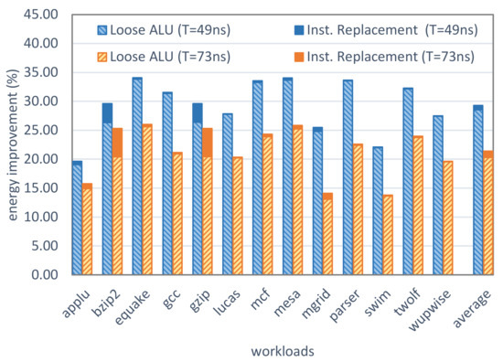
Figure 13.
Energy improvement over the baseline (Tight ALU). The additional improvement is also calculated for when addition/subtract instructions are replaced by increment/decrement instructions when possible (clock period is 73 and 49 ns).
5.4.3. High-Level Optimization Improvements
Whenever fast instructions are more utilized by a workload, the energy improvements are even higher. This concept can be incorporated at a higher level to perform application and compiler optimization, which further improves energy efficiency and performance. This can be done in various ways, as discussed in Section 4.2.3.
Our analysis of the ALU instruction stream shows that in some workloads, a number of add/subtract instructions can be replaced by increment/decrement. In workloads such as “bzip2” and “gzip”, which utilizes add and subtract a lot, it is possible to change up to 11% of all instructions to increment/decrement. Since increment/decrement instructions are faster compared to add/subtract instructions, the improvement in energy and performance is considerable for these types of workloads. The energy improvements and the boost from applying the instruction replacement are depicted in Figure 13 for two clock periods: 73 ns (all instructions are executed in at most two clock cycles) and 49 ns (three clock cycles). For 49 ns, the energy and performance improvements are 3% and 4.3% higher for “bzip2” and “gzip” when the instruction replacement technique is applied. The technique is still applicable to other workloads; however, the improvements are less (approximately 1%). Applying the instruction replacement technique increases the average energy and performance improvements to 29.3% and 12.8% when the clock period is 49 ns (21.4% and 2.4% on average when the clock period is 73 ns).
In order to show the benefits of data type conversion, we executed a simple “matrix manipulation” application, which calculates for given matrices and . The corresponding results are presented in Table 1 for two clock periods: 73 and 49 ns. With a clock period of 49 ns and 2-byte data type used for “matrix manipulation”, the energy and performance improvements of the multi-cycled Loose ALU over the baseline are 26.5% and 8.6%, respectively. However, changing the data type to a 1-byte data type increases the energy and performance improvements to 29.0% and 12% over the baseline.

Table 1.
Energy and performance improvements of executing the “matrix manipulation” workload with different data types.
Furthermore, the 1-byte data type is inherently more energy-efficient compared to the 2-byte data type (22.5 nJ vs. 27.9 nJ). Therefore, the cumulative energy improvement of changing the data type from 2-byte data type to 1-byte data type is 42.9% (going from 27.9 to 15.9 nJ). Additionally, the performance also improves by 29.2% (going from 502 to 356 s).
In summary, high-level optimization methods, such as instruction replacement and data type conversion, can be used to increase the benefits from the proposed instruction multi-cycling. However, the energy and performance improvement obtained by these methods is highly dependent on the executed workload.
5.4.4. Energy/Performance/Reliability Trade-Off
In the near-threshold voltage region, each instruction has a much wider delay distribution compared to the super-threshold region with a longer tail. Therefore, changing the clock period affects the tail of the distribution contributing to failures. We calculate the failure probability for each clock period according to Equation (15) and obtain the reliability improvement as the ratio of the failure probability between the baseline and the optimized ALU:
The reliability improvement is depicted in Figure 12b versus the clock period. There are points where the reliability improvement worsens, which are mostly points with very high energy and performance improvement. This is due to the fact that for these points of clock periods the timing margins of most of the instructions are very small, leading to a significant probability of failure even larger than the baseline. However, there are several points with orders of magnitude better reliability. For example, the reliability improvement ratio is ≈ when the clock period is 57.7 ns or 22,891 when the clock period is 71.5 ns. The performance and energy improvement is also significant in these points. The reason for such large reliability improvements is that the baseline has many critical or near-critical instructions with zero or minimal slack. However, the multi-cycling strategy is able to provide enough timing margin for many instructions such that the provided time for the execution of each instruction marks very high sigma values on the tails of all the delay distributions. Therefore, the designer is able to find a good trade-off among energy efficiency, performance and reliability according to the design requirements.
5.4.5. Discussion
It is evident from the results analyzed before that the multi-cycling approach can provide considerable energy and performance benefits, as well as reliability improvements. However, these results represent the ideal case where the clock period can be adjusted without any constraints.
In a real processor (or an ASIC), there may be other timing critical components, limiting the freedom for modifying the clock period. Hence, another operation point in Figure 12b might be chosen. In such scenarios, the entire processor has to operate at a higher frequency in order to exploit a short clock period for the ALU. This may require additional design tweaks for other parts of the processor. For this purpose, timing critical components of the processor can be split up into multiple “short-cycle” components. Consequently, this results in a deeper pipeline, requiring more control logic and more registers. However, this overhead should be compensated by the overall leakage savings of the entire processor due to the runtime benefits of our novel multi-cycling approach. In case a multi-cycle instruction has to be executed by the ALU, the pipeline frontend of the microprocessor is stopped (through using a no-operation instruction, or clock gating), such that the ALU can work for multiple cycles without change of the input vector.
An alternative solution is to execute multiple short instructions in the ALU per clock cycle. By that means, no major modifications of other processor components are necessary. For instance, to execute two instructions in a clock cycle, the high and low levels of the clock signal can be exploited as it was done in the Intel Pentium 4 [121]. Executing more than two instructions in one cycle requires additional shifted clock signals. Therefore, this scheme is only feasible for processors featuring reservation stations to execute multiple instructions per clock cycle.
In an energy efficient design, the operands of a functional unit are loaded from the memory before the functional unit starts executing the instruction, in order to improve power consumption and performance. These operands are typically stored in the local registers, which are easily accessible by the functional unit without much latency. As an example, the registers at the I/O of an ALU in a pipelined processor store the operands used by the ALU.
5.5. Functional Unit Partitioning Results
This section presents the results of applying the proposed functional unit partitioning to an ALU, based on the simulation setup presented in Section 5.3.
5.5.1. Clustering Results
The distance metrics are extracted based on the analysis of the SPEC benchmark workloads. The temporal distance metric is extracted for = 100. The dendrogram in Figure 14 illustrates the results of the AHC method. As shown in this figure, most of the rarely used instructions in Figure 9 are either grouped together or grouped with other closely similar structures. The original ALU can be partitioned into n smaller ALUs according to the dendrogram. One can determine the best n value, based on inconsistency coefficients [122]. However, as the overhead of hardware implementation increases with the number of clusters, we only have to limit n to have at most four clusters (ALUs). Here, we present results for partitioning the ALU into three and four smaller ALUs as the energy improvement for two ALUs vanishes away as the power-gating threshold () increases.
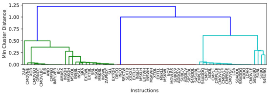
Figure 14.
Dendrogram illustration of the proposed AHC method for some of the instructions. The instructions are merged bottom-up to form larger clusters.
5.5.2. Circuit-Level Results
Based on the clustering method, the original ALU is partitioned into three ALUs (3-ALU) and four ALUs (4-ALU). Table 2 reports the area overhead and performance improvement of the 3-ALU and 4-ALU compared to the original ALU at 14 nm. In the performance improvement calculation, we also considered the delay of the extra multiplexer/demultiplexer circuit for both 4-ALU and 3-ALU designs.

Table 2.
Energy improvement results for 3-ALU and 4-ALU over Original ALU for 14 nm PTM [117].
Both 3-ALU and 4-ALU designs occupy more area compared to the original ALU as expected. The reported area overhead is the increase in the overall ALU area in percentage, considering all additional circuits. Please note that in modern processors, the die area is dominated by memory elements [123]; hence, the increased ALU area does not contribute to a significant change in the overall die area. On the other hand, these ALUs are faster than the original ALU because the logic implemented in each of the partitioned ALUs is simpler and more coherent. By reducing the supply voltage, the performance gain diminishes slowly, because the impact of process variation on the shorter critical paths of smaller ALUs is more than the long critical path in the original ALU.
Additionally, the overall energy improvement achieved by the proposed ALU partitioning method is extracted and reported in Table 2. This is done by calculating the percentage of the time that each smaller ALU can be power-gated based on a given power-gating threshold () and for each workload. As presented in Table 2, there is a significant energy improvement even in the super-threshold region ( V). The reason is that one of the partitioned ALUs is mostly in sleep mode because its instructions are rarely used (see Figure 9 and Figure 14). The percentage of the time an ALU is power-gated for a specific is the same for all supply voltages; however, the energy improvement by the proposed ALU partitioning technique is slightly more at lower supply voltages. The reason is that the leakage power contribution to the overall power consumption grows significantly by reducing the supply voltage. Therefore, reducing the same amount of leakage results in a larger percentage of energy saving at lower supply voltages.
Figure 15 compares the energy improvement results for 4-ALU at near-threshold region ( V) in two technology nodes: 10 and 14 nm. As shown, the energy improvement results for these technology nodes resemble each other closely. A similar trend is observed for the rest of the results.
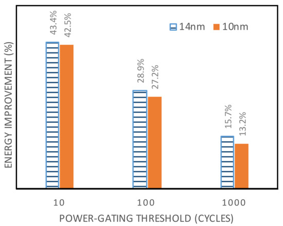
Figure 15.
Energy improvement of functional unit partitioning, on an ALU partitioned into 4 smaller units (4-ALU), for 10 and 14 nm technology nodes.
5.5.3. Performance and Reliability Trade-Off
The performance improvement of the functional unit partitioning, shown in Table 2, could be traded for reliability at low supply voltages, similar to what was explained for instruction multi-cycling in Section 5.4.
According to the results, it is possible to enjoy maximum performance improvement (for example 11% at V) or invest the achieved speed on reliability to get up to times lower failure probability. At the near-threshold supply voltage ( V) the maximum achievable reliability improvement is 11.5× (by trading 7% performance improvement from Table 2) because the delay distribution of the union ALU becomes wider than the original ALU due to its shorter critical path.
6. Summary
The assumptions and optimization targets for NTC circuit design are different from the conventional super-threshold design, due to large impact of variabilities as well as comparable contributions of leakage power and dynamic power. This paper presented two cross-layer design optimization approaches for NTC circuits to co-optimize energy-efficiency, reliability, and performance.
In the instruction multi-cycling approach, the idle time of the functional units is reduced by executing slow instructions in multiple clock cycles and fast instructions in one clock cycle. This approach consists of circuit redesign for smoother slack distribution across instructions (circuit level), multi-cycle execution of slow instructions (architecture level) and code replacement (compiler level). Our experimental results show that this approach achieves significant energy (34%) and performance (19%) improvement while providing orders of magnitude reduction of timing failure rate.
The proposed functional unit partitioning approach improves the energy efficiency and reliability of functional units by exploiting fine-grained power-gating. For this purpose, a large functional unit like an ALU is partitioned into several smaller (and faster) units based on the instruction usage pattern of the running applications and inherent similarity of the instructions. As a result, the smaller functional units can be power-gated whenever they are not used for a long time. Our simulation results show that the energy efficiency of an ALU can be improved by up to 43.4% in the NTV region. Additionally, the performance can be improved by at least 7.0%, or the reliability can be improved by 11.5 times in the NTV region.
Therefore, by revisiting the design of functional units as important components of data paths and utilizing cross-layer approaches, it is possible to optimize the energy-efficiency, performance, and reliability of NTC designs.
Author Contributions
Conceptualization and methodology, M.S.G. and M.T. All authors have read and agreed to the published version of the manuscript.
Funding
This research received no external funding.
Conflicts of Interest
The authors declare no conflict of interest.
References
- Moore, G. Cramming more components onto integrated circuits. Electronics 1965, 38, 114–117. [Google Scholar] [CrossRef]
- Moore, G.E. Progress in digital integrated electronics. In Proceedings of the International Electron Devices Meeting (IEDM), Washington, DC, USA, 1–3 December 1975; Volume 21, pp. 11–13. [Google Scholar]
- Brock, D.C.; Moore, G.E. Understanding Moore’s Law: Four Decades of Innovation; Chemical Heritage Foundation: Philadelphia, PA, USA, 2006. [Google Scholar]
- Borkar, S. Design challenges of technology scaling. IEEE Micro 1999, 19, 23–29. [Google Scholar] [CrossRef]
- Bohr, M. The new era of scaling in an SoC world. In Proceedings of the International Solid-State Circuits Conference (ISSCC), San Francisco, CA, USA, 8–12 February 2009; pp. 23–28. [Google Scholar]
- International Technology Roadmap for Semiconductors (ITRS). Available online: http://www.itrs2.net (accessed on 17 August 2020).
- International Roadmap for Devices and Systems (IRDS). Available online: https://irds.ieee.org (accessed on 17 August 2020).
- Dennard, R.H.; Gaensslen, F.H.; Rideout, V.L.; Bassous, E.; LeBlanc, A.R. Design of ion-implanted MOSFET’s with very small physical dimensions. IEEE J. Solid State Circuits 1974, 9, 256–268. [Google Scholar] [CrossRef]
- Bohr, M. A 30 year retrospective on Dennard’s MOSFET scaling paper. IEEE Solid State Circuits Soc. Newsl. 2007, 12, 11–13. [Google Scholar] [CrossRef]
- Borkar, S.; Chien, A.A. The Future of Microprocessors. Commun. ACM 2011, 54, 67–77. [Google Scholar] [CrossRef]
- Esmaeilzadeh, H.; Blem, E.; Amant, R.S.; Sankaralingam, K.; Burger, D. Dark silicon and the end of multicore scaling. In Proceedings of the International Symposium on Computer Architecture (ISCA), San Jose, CA, USA, 4–8 June 2011; pp. 365–376. [Google Scholar]
- Chang, L.; Frank, D.J.; Montoye, R.K.; Koester, S.J.; Ji, B.L.; Coteus, P.W.; Dennard, R.H.; Haensch, W. Practical Strategies for Power-Efficient Computing Technologies. Proc. IEEE 2010, 98, 215–236. [Google Scholar] [CrossRef]
- Esmaeilzadeh, H.; Blem, E.; St. Amant, R.; Sankaralingam, K.; Burger, D. Power Limitations and Dark Silicon Challenge the Future of Multicore. ACM Trans. Comput. Syst. (TOCS) 2012, 30, 1–27. [Google Scholar] [CrossRef]
- Evans, D. The Internet of Things: How the Next Evolution of the Internet Is Changing Everything. In CISCO White Paper; Cisco IBSG: San Jose, CA, USA, 2011; pp. 1–11. [Google Scholar]
- Ericsson, A. Enabling the internet of things. In Ericsson Mobility Report: On the Pulse of the Networked Society; Ericsson AB: Stockholm, Sweden, 2015; p. 10. [Google Scholar]
- Middleton, P. Forecast Analysis: Internet of Things—Endpoints, Worldwide, 2016 Update. 2017. Available online: https://www.gartner.com/en/documents/3841268/forecast-analysis-internet-of-things-endpoints-worldwide (accessed on 2 November 2020).
- Avgerinou, M.; Bertoldi, P.; Castellazzi, L. Trends in data centre energy consumption under the European code of conduct for data centre energy efficiency. Energies 2017, 10, 1470. [Google Scholar] [CrossRef]
- Pedram, M. Power minimization in IC design: Principles and applications. ACM TRansactions Des. Autom. Electron. Syst. (TODAES) 1996, 1, 3–56. [Google Scholar] [CrossRef]
- Pedram, M. Low power design methodologies and techniques: An overview. Microprocess. Rep. 1999, 486, 66. [Google Scholar]
- Tiwari, V.; Singh, D.; Rajgopal, S.; Mehta, G.; Patel, R.; Baez, F. Reducing Power in High-performance Microprocessors. In Proceedings of the Design Automation Conference (DAC), San Francisco, CA, USA, 15–19 June 1998; pp. 732–737. [Google Scholar]
- Semeraro, G.; Magklis, G.; Balasubramonian, R.; Albonesi, D.H.; Dwarkadas, S.; Scott, M.L. Energy-efficient processor design using multiple clock domains with dynamic voltage and frequency scaling. In Proceedings of the International Symposium on High-Performance Computer Architecture (HPCA), Cambridge, MA, USA, 2–6 February 2002; pp. 29–40. [Google Scholar]
- Burd, T.D.; Pering, T.A.; Stratakos, A.J.; Brodersen, R.W. A dynamic voltage scaled microprocessor system. IEEE J. Solid State Circuits 2000, 35, 1571–1580. [Google Scholar] [CrossRef]
- Chandrakasan, A.P.; Sheng, S.; Brodersen, R.W. Low-power CMOS digital design. IEEE J. Solid State Circuits 1992, 27, 473–484. [Google Scholar] [CrossRef]
- Soeleman, H.; Roy, K.; Paul, B.C. Robust subthreshold logic for ultra-low power operation. IEEE Trans. Very Large Scale Integr. (VLSI) Syst. 2001, 9, 90–99. [Google Scholar] [CrossRef]
- Gonzalez, R.; Gordon, B.M.; Horowitz, M.A. Supply and threshold voltage scaling for low power CMOS. IEEE J. Solid State Circuits 1997, 32, 1210–1216. [Google Scholar] [CrossRef]
- Jain, S.; Khare, S.; Yada, S.; Ambili, V.; Salihundam, P.; Ramani, S.; Muthukumar, S.; Srinivasan, M.; Kumar, A.; Gb, S.K.; et al. A 280 mV-to-1.2 V wide-operating-range IA-32 processor in 32 nm CMOS. In Proceedings of the International Solid-State Circuits Conference (ISSCC), San Francisco, CA, USA, 19–23 February 2012; pp. 66–68. [Google Scholar]
- Dreslinski, R.G.; Wieckowski, M.; Blaauw, D.; Sylvester, D.; Mudge, T. Near-threshold computing: Reclaiming moore’s law through energy efficient integrated circuits. Proc. IEEE 2010, 98, 253–266. [Google Scholar] [CrossRef]
- Kaul, H.; Anders, M.A.; Mathew, S.K.; Hsu, S.K.; Agarwal, A.; Krishnamurthy, R.K.; Borkar, S. A 320 mv 56 μw 411 gops/watt ultra-low voltage motion estimation accelerator in 65 nm cmos. IEEE J. Solid State Circuits 2009, 44, 107–114. [Google Scholar] [CrossRef]
- Pahlevan, A.; Picorel, J.; Zarandi, A.P.; Rossi, D.; Zapater, M.; Bartolini, A.; Del Valle, P.G.; Atienza, D.; Benini, L.; Falsafi, B. Towards near-threshold server processors. In Proceedings of the Design, Automation & Test in Europe Conference (DATE), Dresden, Germany, 14–18 March 2016; pp. 7–12. [Google Scholar]
- Dreslinski, R., Jr. Near Threshold Computing: From Single Core to Many-Core Energy Efficient Architectures. Ph.D. Thesis, University of Michigan, Ann Arbor, MI, USA, 2011. [Google Scholar]
- De, V. Fine-grain power management in manycore processor and System-on-Chip (SoC) designs. In Proceedings of the International Conference on Computer-Aided Design (ICCAD), Austin, TX, USA, 2–6 November 2015; pp. 159–164. [Google Scholar]
- Zhai, B.; Dreslinski, R.G.; Blaauw, D.; Mudge, T.; Sylvester, D. Energy Efficient Near-threshold Chip Multi-processing. In Proceedings of the International Symposium on Low Power Electronics and Design (ISLPED), Portland, OR, USA, 27–29 August 2007; pp. 32–37. [Google Scholar]
- Kaul, H.; Anders, M.; Hsu, S.; Agarwal, A.; Krishnamurthy, R.; Borkar, S. Near-threshold voltage (NTV) design: Opportunities and challenges. In Proceedings of the Design Automation Conference (DAC), San Francisco, CA, USA, 3–7 June 2012; pp. 1153–1158. [Google Scholar]
- Alidina, M.; Monteiro, J.; Devadas, S.; Ghosh, A.; Papaefthymiou, M. Precomputation-based sequential logic optimization for low power. IEEE Trans. Very Large Scale Integr. (VLSI) Syst. 1994, 2, 426–436. [Google Scholar] [CrossRef]
- Benini, L.; De Micheli, G.; Macii, E. Designing low-power circuits: Practical recipes. IEEE Circuits Syst. Mag. 2001, 1, 6–25. [Google Scholar] [CrossRef]
- Wei, L.; Chen, Z.; Johnson, M.; Roy, K.; De, V. Design and optimization of low voltage high performance dual threshold CMOS circuits. In Proceedings of the Design Automation Conference (DAC), San Francisco, CA, USA, 15–19 June 1998; pp. 489–494. [Google Scholar]
- Fujiwara, F.B. A Neutral Netlist of 10 Combinational Benchmark Circuits. In Proceedings of the International Symposium on Circuits and Systems (ISCAS), Kyoto, Japan, 5–7 June 1985; pp. 695–698. [Google Scholar]
- Brglez, F.; Pownall, P.; Hum, R. Accelerated ATPG and fault grading via testability analysis. In Proceedings of the International Symposium on Circuits and Systems (ISCAS), Kyoto, Japan, 5–7 June 1985; pp. 695–698. [Google Scholar]
- Sakurai, T.; Newton, A.R. Alpha-power law MOSFET model and its applications to CMOS inverter delay and other formulas. IEEE J. Solid State Circuits 1990, 25, 584–594. [Google Scholar] [CrossRef]
- Markovic, D.; Wang, C.C.; Alarcon, L.P.; Liu, T.; Rabaey, J.M. Ultralow-Power Design in Near-Threshold Region. Proc. IEEE 2010, 98, 237–252. [Google Scholar] [CrossRef]
- Enz, C.C.; Krummenacher, F.; Vittoz, E.A. An analytical MOS transistor model valid in all regions of operation and dedicated to low-voltage and low-current applications. Analog. Integr. Circuits Signal Process. 1995, 8, 83–114. [Google Scholar] [CrossRef]
- Bucher, M.; Bazigos, A.; Krummenacher, F.; Sallese, J.M.; Enz, C. EKV3. 0: An advanced charge based MOS transistor model. A design-oriented MOS transistor compact model. In Transistor Level Modeling for Analog/RF IC Design; Springer: Berlin/Heidelberg, Germany, 2006; pp. 67–95. [Google Scholar]
- Keller, S.; Harris, D.M.; Martin, A.J. A compact transregional model for digital CMOS circuits operating near threshold. IEEE Trans. Very Large Scale Integr. (VLSI) Syst. 2014, 22, 2041–2053. [Google Scholar] [CrossRef]
- Drego, N.; Chandrakasan, A.; Boning, D. Lack of spatial correlation in MOSFET threshold voltage variation and implications for voltage scaling. IEEE Trans. Semicond. Manuf. 2009, 22, 245–255. [Google Scholar] [CrossRef]
- Hanson, S.; Zhai, B.; Bernstein, K.; Blaauw, D.; Bryant, A.; Chang, L.; Das, K.K.; Haensch, W.; Nowak, E.J.; Sylvester, D.M. Ultralow-voltage, minimum-energy CMOS. IBM J. Res. Dev. 2006, 50, 469–490. [Google Scholar] [CrossRef]
- Kiamehr, S.; Ebrahimi, M.; Golanbari, M.S.; Tahoori, M.B. Temperature-aware dynamic voltage scaling to improve energy efficiency of near-threshold computing. IEEE Trans. Very Large Scale Integr. (VLSI) Syst. 2017, 25, 2017–2026. [Google Scholar] [CrossRef]
- Krishnamurthy, R.K.; Himanshu, K. Ultra-low voltage technologies for energy-efficient special-purpose hardware accelerators. Intel Technol. J. 2009, 13, 102–117. [Google Scholar]
- Bowman, K.; Tschanz, J.; Wilkerson, C.; Lu, S.L.; Karnik, T.; De, V.; Borkar, S. Circuit techniques for dynamic variation tolerance. In Proceedings of the Design Automation Conference (DAC), San Francisco, CA, USA, 26–31 July 2009; pp. 4–7. [Google Scholar]
- Ernst, D.; Das, S.; Lee, S.; Blaauw, D.; Austin, T.; Mudge, T.; Kim, N.S.; Flautner, K. Razor: Circuit-level correction of timing errors for low-power operation. IEEE Micro 2004, 24, 10–20. [Google Scholar] [CrossRef]
- Greskamp, B.; Torrellas, J. Paceline: Improving single-thread performance in nanoscale CMPs through core overclocking. In Proceedings of the International Conference on Parallel Architecture and Compilation Techniques (IEEE Computer Society), Brasov, Romania, 15–19 September 2007; pp. 213–224. [Google Scholar]
- Ramasubramanian, S.G.; Venkataramani, S.; Parandhaman, A.; Raghunathan, A. Relax-and-retime: A methodology for energy-efficient recovery based design. In Proceedings of the Design Automation Conference (DAC), Austin, TX, USA, 2–6 June 2013; p. 111. [Google Scholar]
- Liu, Y.; Ye, R.; Yuan, F.; Kumar, R.; Xu, Q. On logic synthesis for timing speculation. In Proceedings of the International Conference on Computer-Aided Design (ICCAD), San Jose, CA, USA, 5–8 November 2012; pp. 591–596. [Google Scholar]
- Golanbari, M.S.; Kiamehr, S.; Tahoori, M.B. Hold-time Violation Analysis and Fixing in Near-Threshold Region. In Proceedings of the International Workshop on Power and Timing Modeling, Optimization and Simulation (PATMOS), Bremen, Germany, 21–23 September 2016. [Google Scholar]
- Zhai, B.; Hanson, S.; Blaauw, D.; Sylvester, D. A variation-tolerant sub-200 mV 6-T subthreshold SRAM. IEEE J. Solid State Circuits 2008, 43, 2338. [Google Scholar] [CrossRef]
- Chang, L.; Montoye, R.K.; Nakamura, Y.; Batson, K.A.; Eickemeyer, R.J.; Dennard, R.H.; Haensch, W.; Jamsek, D. An 8T-SRAM for variability tolerance and low-voltage operation in high-performance caches. IEEE J. Solid State Circuits 2008, 43, 956–963. [Google Scholar] [CrossRef]
- Chang, L.; Fried, D.M.; Hergenrother, J.; Sleight, J.W.; Dennard, R.H.; Montoye, R.K.; Sekaric, L.; McNab, S.J.; Topol, A.W.; Adams, C.D.; et al. Stable SRAM cell design for the 32 nm node and beyond. In Symposium on VLSI Technology; IEEE: Piscataway, NJ, USA, 2005; pp. 128–129. [Google Scholar]
- Kulkarni, J.P.; Kim, K.; Roy, K. A 160 mV, fully differential, robust schmitt trigger based sub-threshold SRAM. In Proceedings of the International Symposium on Low Power Electronics and Design (ISLPED), Portland, OR, USA, 27–29 August 2007; pp. 171–176. [Google Scholar]
- Calhoun, B.H.; Chandrakasan, A. A 256kb sub-threshold SRAM in 65nm CMOS. In Proceedings of the International Solid-State Circuits Conference (ISSCC), San Francisco, CA, USA, 6–9 February 2006; pp. 2592–2601. [Google Scholar]
- Hu, J.; Yu, X. Low voltage and low power pulse flip-flops in nanometer CMOS processes. Curr. Nanosci. 2012, 8, 102–107. [Google Scholar] [CrossRef]
- Pinckney, N.; Blaauw, D.; Sylvester, D. Low-power near-threshold design: Techniques to improve energy efficiency. IEEE Solid State Circuits Mag. 2015, 7, 49–57. [Google Scholar] [CrossRef]
- Fuketa, H.; Hirairi, K.; Yasufuku, T.; Takamiya, M.; Nomura, M.; Shinohara, H.; Sakurai, T. 12.7-times energy efficiency increase of 16-bit integer unit by power supply voltage (V DD) scaling from 1.2 V to 310 mV enabled by contention-less flip-flops (CLFF) and separated V DD between flip-flops and combinational logics. In Proceedings of the International Symposium on Low Power Electronics and Design (ISLPED), Fukuoka, Japan, 1–3 August 2011; pp. 163–168. [Google Scholar]
- Chandra, V.; Aitken, R. Impact of technology and voltage scaling on the soft error susceptibility in nanoscale CMOS. In Proceedings of the IEEE International Symposium on Defect and Fault Tolerance of VLSI Systems, Boston, MA, USA, 1–3 October 2008; pp. 114–122. [Google Scholar]
- Cannon, E.H.; Reinhardt, D.D.; Gordon, M.S.; Makowenskyj, P.S. SRAM SER in 90, 130 and 180 nm bulk and SOI technologies. In Proceedings of the IEEE International Reliability Physics Symposium Proceedings (IRPS), Phoenix, AZ, USA, 25–29 April 2004; pp. 300–304. [Google Scholar]
- Hazucha, P.; Karnik, T.; Walstra, S.; Bloechel, B.A.; Tschanz, J.W.; Maiz, J.; Soumyanath, K.; Dermer, G.E.; Narendra, S.; De, V.; et al. Measurements and analysis of SER-tolerant latch in a 90-nm dual-V/sub T/CMOS process. IEEE J. Solid State Circuits 2004, 39, 1536–1543. [Google Scholar] [CrossRef]
- Naseer, R.; Draper, J. DF-DICE: A scalable solution for soft error tolerant circuit design. In Proceedings of the International Symposium on Circuits and System (ISCAS), Island of Kos, Greece, 21–24 May 2006; pp. 3890–3893. [Google Scholar]
- Zhang, M.; Mitra, S.; Mak, T.; Seifert, N.; Wang, N.J.; Shi, Q.; Kim, K.S.; Shanbhag, N.R.; Patel, S.J. Sequential element design with built-in soft error resilience. IEEE Trans. Very Large Scale Integr. (VLSI) Syst. 2006, 14, 1368–1378. [Google Scholar] [CrossRef]
- Zhou, Q.; Mohanram, K. Transistor sizing for radiation hardening. In Proceedings of the International Reliability Physics Symposium (IRPS), Phoenix, AZ, USA, 25–29 April 2004; pp. 310–315. [Google Scholar]
- Ebrahimi, M.; Rao, P.M.B.; Seyyedi, R.; Tahoori, M.B. Low-cost multiple bit upset correction in SRAM-based FPGA configuration frames. IEEE Trans. Very Large Scale Integr. (VLSI) Syst. 2016, 24, 932–943. [Google Scholar] [CrossRef]
- Chang, I.J.; Kim, J.J.; Park, S.P.; Roy, K. A 32 kb 10T sub-threshold SRAM array with bit-interleaving and differential read scheme in 90 nm CMOS. IEEE J. Solid State Circuits 2009, 44, 650–658. [Google Scholar] [CrossRef]
- Fu, X.; Li, T.; Fortes, J.A.B. Soft error vulnerability aware process variation mitigation. In Proceedings of the International Symposium on High Performance Computer Architecture (HPCA), Raleigh, NC, USA, 14–18 February 2009; pp. 93–104. [Google Scholar]
- Golanbari, M.S. Design and Optimization for Resilient Energy Efficient Computing. Ph.D. Thesis, Karlsruher Institut für Technologie (KIT), Karlsruhe, Germany, 2019. [CrossRef]
- Markov, S.; Zain, A.S.M.; Cheng, B.; Asenov, A. Statistical variability in scaled generations of n-channel UTB-FD-SOI MOSFETs under the influence of RDF, LER, OTF and MGG. In Proceedings of the IEEE International SOI Conference (SOI), Napa, CA, USA, 1–4 October 2012; pp. 1–2. [Google Scholar]
- Seok, M.; Chen, G.; Hanson, S.; Wieckowski, M.; Blaauw, D.; Sylvester, D. CAS-FEST 2010: Mitigating variability in near-threshold computing. IEEE J. Emerg. Sel. Top. Circuits Syst. 2011, 1, 42–49. [Google Scholar] [CrossRef]
- Hanson, S.; Zhai, B.; Seok, M.; Cline, B.; Zhou, K.; Singhal, M.; Minuth, M.; Olson, J.; Nazhandali, L.; Austin, T.; et al. Performance and variability optimization strategies in a sub-200 mV, 3.5 pJ/inst, 11nW subthreshold processor. In IEEE Symposium on VLSI Circuits; IEEE: Piscataway, NJ, USA, 2007; pp. 152–153. [Google Scholar]
- Kakoee, M.R.; Sathanur, A.; Pullini, A.; Huisken, J.; Benini, L. Automatic synthesis of near-threshold circuits with fine-grained performance tunability. In Proceedings of the International Symposium on Low Power Electronics and Design (ISLPED), Austin, TX, USA, 18–20 August 2010; pp. 401–406. [Google Scholar]
- Myers, J.; Savanth, A.; Gaddh, R.; Howard, D.; Prabhat, P.; Flynn, D. A subthreshold ARM cortex-M0+ subsystem in 65 nm CMOS for WSN applications with 14 power domains, 10T SRAM, and integrated voltage regulator. IEEE J. Solid State Circuits 2016, 51, 31–44. [Google Scholar]
- Karpuzcu, U.R.; Kim, N.S.; Torrellas, J. Coping with parametric variation at near-threshold voltages. IEEE Micro 2013, 33, 6–14. [Google Scholar] [CrossRef]
- Kim, S.; Kwon, I.; Fick, D.; Kim, M.; Chen, Y.P.; Sylvester, D. Razor-lite: A side-channel error-detection register for timing-margin recovery in 45nm SOI CMOS. In Proceedings of the International Solid-State Circuits Conference (ISSCC), San Francisco, CA, USA, 17–21 February 2013; pp. 264–265. [Google Scholar]
- Austin, T.; Bertacco, V.; Blaauw, D.; Mudge, T. Opportunities and challenges for better than worst-case design. In Proceedings of the Asia and South Pacific Design Automation Conference (ASP-DAC), Shanghai, China, 18–21 January 2005; pp. 2–7. [Google Scholar]
- Gebregiorgis, A.; Bishnoi, R.; Tahoori, M.B. A Comprehensive Reliability Analysis Framework for NTC Caches: A System to Device Approach. IEEE Trans. Comput. Aided Des. Integr. Circuits Syst. 2018, 38, 439–452. [Google Scholar] [CrossRef]
- Zhai, B.; Pant, S.; Nazhandali, L.; Hanson, S.; Olson, J.; Reeves, A.; Minuth, M.; Helfand, R.; Austin, T.; Sylvester, D.; et al. Energy-efficient subthreshold processor design. IEEE Trans. Very Large Scale Integr. (VLSI) Syst. 2009, 17, 1127–1137. [Google Scholar] [CrossRef]
- Gebregiorgis, A.; Golanbari, M.S.; Kiamehr, S.; Oboril, F.; Tahoori, M.B. Maximizing Energy Efficiency in NTC by Variation-Aware Microprocessor Pipeline Optimization. In Proceedings of the International Symposium on Low Power Electronics and Design (ISLPED), San Francisco, CA, USA, 8–10 August 2016; pp. 272–277. [Google Scholar]
- Zhai, B.; Hanson, S.; Blaauw, D.; Sylvester, D. Analysis and mitigation of variability in subthreshold design. In Proceedings of the International Symposium on Low Power Electronics and Design (ISLPED), San Diego, CA, USA, 8–10 August 2005; pp. 20–25. [Google Scholar]
- Gebregiorgis, A.; Tahoori, M.B. Fine-Grained Energy-Constrained Microprocessor Pipeline Design. IEEE Trans. Very Large Scale Integr. (VLSI) Syst. 2018, 26, 457–469. [Google Scholar] [CrossRef]
- Nazhandali, L.; Zhai, B.; Olson, J.; Reeves, A.; Minuth, M.; Helfand, R.; Pant, S.; Austin, T.; Blaauw, D. Energy optimization of subthreshold-voltage sensor network processors. ACM Sigarch Comput. Archit. News 2005, 33, 197–207. [Google Scholar] [CrossRef]
- Ramadass, Y.K.; Chandrakasan, A.P. Minimum energy tracking loop with embedded DC–DC converter enabling ultra-low-voltage operation down to 250 mV in 65 nm CMOS. IEEE J. Solid State Circuits 2008, 43, 256–265. [Google Scholar] [CrossRef]
- Ikenaga, Y.; Nomura, M.; Nakazawa, Y.; Hagihara, Y. A circuit for determining the optimal supply voltage to minimize energy consumption in LSI circuit operations. IEEE J. Solid State Circuits 2008, 43, 911–918. [Google Scholar] [CrossRef]
- Koskinen, L.; Hiienkari, M.; Mäkipää, J.; Turnquist, M.J. Implementing minimum-energy-point systems with adaptive logic. IEEE Trans. Very Large Scale Integr. (VLSI) Syst. 2016, 24, 1247–1256. [Google Scholar] [CrossRef]
- Mehta, N.; Makinwa, K.A. Minimum energy point tracking for sub-threshold digital CMOS circuits using an in-situ energy sensor. In Proceedings of the International Symposium on Circuits and Systems (ISCAS), Beijing, China, 19–23 May 2013; pp. 570–573. [Google Scholar]
- Mehta, N.; Amrutur, B. Dynamic supply and threshold voltage scaling for CMOS digital circuits using in-situ power monitor. IEEE Trans. Very Large Scale Integr. (VLSI) Syst. 2012, 20, 892–901. [Google Scholar] [CrossRef]
- Wang, A.; Chandrakasan, A.P.; Kosonocky, S.V. Optimal supply and threshold scaling for subthreshold CMOS circuits. In Proceedings of the IEEE Computer Society Annual Symposium on VLSI, Pittsburgh, PA, USA, 25–26 April 2002; pp. 7–11. [Google Scholar]
- Calhoun, B.H.; Wang, A.; Chandrakasan, A. Modeling and sizing for minimum energy operation in subthreshold circuits. IEEE J. Solid State Circuits 2005, 40, 1778–1786. [Google Scholar] [CrossRef]
- Karpuzcu, U.R.; Sinkar, A.; Kim, N.S.; Torrellas, J. EnergySmart: Toward energy-efficient manycores for near-threshold computing. In Proceedings of the International Symposium on High-Performance Computer Architecture (HPCA), Shenzhen, China, 23–27 February 2013; pp. 542–553. [Google Scholar]
- Seo, S.; Dreslinski, R.G.; Woh, M.; Park, Y.; Charkrabari, C.; Mahlke, S.; Blaauw, D.; Mudge, T. Process variation in near-threshold wide SIMD architectures. In Proceedings of the Design Automation Conference (DAC), San Francisco, CA, USA 3–7 June 2012; pp. 980–987. [Google Scholar]
- Wieckowski, M.; Park, Y.M.; Tokunaga, C.; Kim, D.W.; Foo, Z.; Sylvester, D.; Blaauw, D. Timing yield enhancement through soft edge flip-flop based design. In Proceedings of the Custom Integrated Circuits Conference (CICC), San Jose, CA, USA, 21–24 September 2008; pp. 543–546. [Google Scholar]
- Joshi, V.; Blaauw, D.; Sylvester, D. Soft-edge flip-flops for improved timing yield: Design and optimization. In Proceedings of the International Conference on Computer-Aided Design (ICCAD), San Jose, CA, USA, 5–8 November 2007; pp. 667–673. [Google Scholar]
- Gammie, G.; Wang, A.; Chau, M.; Gururajarao, S.; Pitts, R.; Jumel, F.; Engel, S.; Royannez, P.; Lagerquist, R.; Mair, H.; et al. A 45 nm 3.5 g baseband-and-multimedia application processor using adaptive body-bias and ultra-low-power techniques. In Proceedings of the International Solid-State Circuits Conference (ISSCC), San Francisco, CA, USA, 3–7 February 2008; pp. 258–611. [Google Scholar]
- Golanbari, M.S.; Kiamehr, S.; Ebrahimi, M.; Tahoori, M.B. Variation-aware near threshold circuit synthesis. In Proceedings of the Design, Automation & Test in Europe Conference (DATE), Dresden, Germany, 14–18 March 2016. [Google Scholar]
- Krimer, E.; Pawlowski, R.; Erez, M.; Chiang, P. Synctium: A near-threshold stream processor for energy-constrained parallel applications. IEEE Comput. Archit. Lett. 2010, 9, 21–24. [Google Scholar] [CrossRef]
- Oboril, F.; Firouzi, F.; Kiamehr, S.; Tahoori, M.B. Negative bias temperature instability-aware instruction scheduling: A cross-layer approach. J. Low Power Electron. 2013, 9, 389–402. [Google Scholar] [CrossRef]
- Oboril, F.; Firouzi, F.; Kiamehr, S.; Tahoori, M. Reducing NBTI-induced processor wearout by exploiting the timing slack of instructions. In Proceedings of the Eighth IEEE/ACM/IFIP International Conference on Hardware/Software Codesign and System Synthesis, Tampere, Finland, 7–12 October 2012; pp. 443–452. [Google Scholar]
- Annavaram, M. A case for guarded power gating for multi-core processors. In Proceedings of the International Symposium on High-Performance Computer Architecture (HPCA), San Antonio, TX, USA, 12–16 February 2011. [Google Scholar]
- Leverich, J.; Monchiero, M.; Talwar, V.; Ranganathan, P.; Kozyrakis, C. Power management of datacenter workloads using per-core power gating. Comput. Archit. Lett. 2009, 8, 48–51. [Google Scholar] [CrossRef]
- Bose, P.; Buyuktosunoglu, A.; Darringer, J.A.; Gupta, M.S.; Healy, M.B.; Jacobson, H.; Nair, I.; Rivers, J.A.; Shin, J.; Vega, A.; et al. Power management of multi-core chips: Challenges and pitfalls. In Proceedings of the Design, Automation & Test in Europe Conference (DATE), Dresden, Germany, 12–16 March 2012. [Google Scholar]
- Hu, Z.; Buyuktosunoglu, A.; Srinivasan, V.; Zyuban, V.; Jacobson, H.; Bose, P. Microarchitectural techniques for power gating of execution units. In Proceedings of the International Symposium on Low Power Electronics and Design (ISLPED), Newport Beach, CA, USA, 9–11 August 2004; pp. 32–37. [Google Scholar]
- Golanbari, M.S.; Gebregiorgis, A.; Oboril, F.; Kiamehr, S.; Tahoori, M.B. A Cross-Layer Approach for Resiliency and Energy Efficiency in Near Threshold Computing. In Proceedings of the International Conference on Computer-Aided Design (ICCAD), Austin, TX, USA, 7–10 November 2016. [Google Scholar]
- Golanbari, M.S.; Gebregiorgis, A.; Moradi, E.; Kiamehr, S.; Tahoori, M.B. Balancing resiliency and energy efficiency of functional units in ultra-low power systems. In Proceedings of the Asia and South Pacific Design Automation Conference (ASP-DAC), Jeju Island, Korea, 22–25 January 2018. [Google Scholar]
- Kaufman, L.; Rousseeuw, P.J. Finding Groups in Data: An Introduction to Cluster Analysis; John Wiley & Sons: Hoboken, NJ, USA, 2009; Volune 344. [Google Scholar]
- Wang, N.; Wang, H.; Jin, Y.; Ye, J. Integrating operation scheduling and binding for functional unit power-gating in high-level synthesis. In Proceedings of the 2017 IEEE 12th International Conference on ASIC (ASICON), Guiyang, China, 25–28 October 2017; pp. 1129–1132. [Google Scholar]
- Jeon, D.; Seok, M.; Chakrabarti, C.; Blaauw, D.; Sylvester, D. A super-pipelined energy efficient subthreshold 240 MS/s FFT core in 65 nm CMOS. IEEE J. Solid State Circuits 2012, 47, 23–34. [Google Scholar] [CrossRef]
- DeGroot, M.H.; Schervish, M.J. Probability and Statistics; Pearson Education: London, UK, 2012. [Google Scholar]
- Kuhn, K.J.; Giles, M.D.; Becher, D.; Kolar, P.; Kornfeld, A.; Kotlyar, R.; Ma, S.T.; Maheshwari, A.; Mudanai, S. Process technology variation. IEEE Trans. Electron Devices 2011, 58, 2197–2208. [Google Scholar] [CrossRef]
- Wang, N.J.; Quek, J.; Rafacz, T.M.; Patel, S.J. Characterizing the effects of transient faults on a high-performance processor pipeline. In Proceedings of the International Conference on Dependable Systems and Networks, Florence, Italy, 28 June–1 July 2004; pp. 61–70. [Google Scholar]
- Synopsys Design Compiler. Available online: https://www.synopsys.com (accessed on 2 November 2020).
- Cadence Encounter Timing System. Available online: http://www.cadence.com (accessed on 2 November 2020).
- ECSM Specification. Available online: https://www.si2.org (accessed on 2 November 2020).
- Sinha, S.; Yeric, G.; Chandra, V.; Cline, B.; Cao, Y. Exploring sub-20nm FinFET design with predictive technology models. In Proceedings of the Design Automation Conference (DAC), San Francisco, CA, USA, 3–7 June 2012; pp. 283–288. [Google Scholar]
- Synopsys 32/28 nm PDK. Available online: https://www.synopsys.com/community/university-program/teaching-resources.html (accessed on 2 November 2020).
- Cadence Virtuoso Variety Statistical Characterization Solution. Available online: http://www.cadence.com (accessed on 2 November 2020).
- Binkert, N.; Beckmann, B.; Black, G.; Reinhardt, S.K.; Saidi, A.; Basu, A.; Hestness, J.; Hower, D.R.; Krishna, T.; Sardashti, S.; et al. The gem5 simulator. ACM Sigarch Comput. Archit. News 2011, 39, 1–7. [Google Scholar] [CrossRef]
- Hinton, G.; Sager, D.; Upton, M.; Boggs, D.; Group, D.P.; Corp, I. The Microarchitecture of the Pentium 4 Processor. Intel Technol. J. 2001, 1, 2001. [Google Scholar]
- Tan, P.N.; Steinbach, M.; Kumar, V. Introduction to Data Mining; Pearson Education: Delhi, India, 2007. [Google Scholar]
- Karunaratne, M.; Oomann, B. An optimal memory BISR implementation. J. Comput. 2013, 8. [Google Scholar] [CrossRef]
Publisher’s Note: MDPI stays neutral with regard to jurisdictional claims in published maps and institutional affiliations. |
© 2020 by the authors. Licensee MDPI, Basel, Switzerland. This article is an open access article distributed under the terms and conditions of the Creative Commons Attribution (CC BY) license (http://creativecommons.org/licenses/by/4.0/).

