Review

Near-Threshold Voltage Design Techniques for Heterogenous Manycore System-on-Chips

Circuit Research, Intel Labs, Intel Corporation, Hillsboro, OR 97124, USA
*
Author to whom correspondence should be addressed.
J. Low Power Electron. Appl. 2020, 10(2), 16; https://doi.org/10.3390/jlpea10020016
Submission received: 14 April 2020 / Revised: 7 May 2020 / Accepted: 7 May 2020 / Published: 14 May 2020
(This article belongs to the Special Issue Circuits and Systems Advances in Near Threshold Computing)

Abstract

:
Aggressive power supply scaling into the near-threshold voltage (NTV) region holds great potential for applications with strict energy budgets, since the energy efficiency peaks as the supply voltage approaches the threshold voltage (VT) of the CMOS transistors. The improved silicon energy efficiency promises to fit more cores in a given power envelope. As a result, many-core Near-threshold computing (NTC) has emerged as an attractive paradigm. Realizing energy-efficient heterogenous system on chips (SoCs) necessitates key NTV-optimized ingredients, recipes and IP blocks; including CPUs, graphic vector engines, interconnect fabrics and mm-scale microcontroller (MCU) designs. We discuss application of NTV design techniques, necessary for reliable operation over a wide supply voltage range—from nominal down to the NTV regime, and for a variety of IPs. Evaluation results spanning Intel’s 32-, 22- and 14-nm CMOS technologies across four test chips are presented, confirming substantial energy benefits that scale well with Moore’s law.

1. Introduction

Near-threshold computing promises dramatic improvements in energy efficiency. For many CMOS designs, the energy consumption reaches an absolute minimum in the NTV regime that is of the order of magnitude improvement over super-threshold operation [1,2,3]. However, frequency degradation due to aggressive voltage scaling may not be acceptable across all single-threaded or performance-constrained applications. The key challenge is to lock-in this excellent energy efficiency benefit at NTV, while addressing the impacts of (a) loss in silicon frequency, (b) increased performance variations and (c) higher functional failure rates in memory and logic circuits. Enabling digital designs to operate over a wide voltage range is key to achieving the best energy efficiency [2], while satisfying varying application performance demands. To tap the full latent potential of NTC, multi-layered co-optimization approaches that crosscut architecture, devices, design, circuits, tool flows and methodologies, and coupled with fine-grain power management techniques are mandatory to realize NTC circuits and systems in scaled CMOS process nodes.
The overarching goal of this work is to advance NTV computing, demonstrate its energy benefits, to quantify and overcome the barriers that have historically relegated ultralow-voltage operation to niche markets. We present four multi-voltage designs across three technology nodes, featuring many-core SoC building blocks. The IPs demonstrate wide dynamic power-performance range, including reliable NTV regime operation for maximum energy efficiency. Key innovations in NTV circuit design methods and CAD approaches for wide-dynamic range design, including optimizations to design methodology are highlighted.
A design summary for the four NTV silicon prototypes is presented in Table 1. The first design describes an Intel Architecture IA-32 processor fabricated in 32-nm SoC platform technology with 2nd generation high-k/metal gate transistors [4]. The chip is capable of reliable ultra-low voltage operation and energy efficient performance across the wide voltage range from 280 mV to 1.2 V. The CPU (Figure 1a) consists of a Pentium™ class IA-32 core [5] with superscalar in-order pipeline, dynamic branch prediction and 8 KB of separate L1 instruction and data caches. Core logic and memory blocks are powered by independent voltage domains to allow processor core and the memories (L1 caches + microcode ROM) to operate at their individual optimal power levels for best overall energy efficiency. This capability allows the IA core logic to aggressively voltage scale well beyond memory minimum operating voltage (Vmin) limits. A multi-voltage, NTV-aware core design synthesis and performance verification (PV) methodology is employed with measured core operation down to 280 mV sub-threshold regime. A minimum-energy voltage optimum (VOPT) is observed at 450 mV for the NTV-CPU, signifying 4.7× better energy efficiency over VDD-max (1.2 V) operation [6].
Single instruction, multiple data (SIMD) permutation operations are key for maximizing high-performance microprocessor vector data path utilization in multimedia, graphics, and signal processing workloads [7]. The second prototype is a wide dynamic range design (240 mV to 1.2 V), presenting an ultra-low-voltage reconfigurable 4-way to 32-way SIMD vector permutation engine [8] (Figure 1b) consisting of a 32-entry × 256b 3-read/1-write ported register file (RF) with a 256b byte-wise any-to-any permute crossbar for 2-D shuffle operations across a 32 × 32 matrix. The register file with three read ports and one write port is used for vertical shuffle. The permute crossbar is used for horizontal shuffle. The SIMD engine is fabricated in a 22-nm SoC platform technology featuring 3-D tri-gate and high-k/metal gate devices [9]. Tri-gate or FinFET devices offer steeper subthreshold swing and improved short-channel effects and offer better variability and energy efficiency at NTV. The engine incorporates vector flip-flops, stacked min-delay buffers, shared gates to average min-sized transistor variations, and ultra-low-voltage split-output (ULVS) level shifters to improve logic Vmin by 150 mV, while enabling a 9× peak energy efficiency of 585 GOPS/W measured at 260 mV supply voltage and a temperature of 50 °C.
Packet-switched routers are communication systems of choice for modern many-core SoCs [12,13]. The third NTV design describes a 2 × 2 2-D mesh network-on-chip (NoC) fabric (Figure 1c) which incorporates a 6-port, 2-lane packet-switched input-buffered wormhole router as a key building block [10]. The resilient NTV-NoC and router incorporates end-to-end forward error correction code (ECC) and within router recovery from transient timing failures using error-detection sequential (EDS) circuits and a novel architectural flow control units (FLIT) replay scheme. The router operates across a wide frequency (voltage) range from 1 GHz (0.85 V) to 67 MHz (340 mV), dissipating 28.5 mW to 675 μW and achieves 3.3× improvement in energy-efficiency at 400 mV VOPT. The NTV-NoC is fabricated in the same 22-nm SoC technology [9] and achieves 63% higher bandwidths at VOPT over a non-resilient router, when operating beyond the point-of-first failure (PoFF).
The final NTV prototype showcases a wireless sensor node (WSN) platform that integrates a mm-scale, 0.79 mm2 NTV IA-32 Quark™ microcontroller (Figure 1d) (MCU) [14,15], built using a 14-nm 2nd generation tri-gate CMOS process. The WSN platform includes a solar cell, energy harvester, flash memory, sensors and a Bluetooth Low Energy (BLE) radio, to enable always-on always-sensing (AOAS) and advanced edge computing capabilities in Internet-of-Things (IoT) systems [11]. The MCU features four independent voltage-frequency islands (VFI), a low-leakage SRAM array, an on-die oscillator clock source capable of operating at sub-threshold voltage, power-gating and multiple active/sleep states, managed by an integrated power management unit (PMU). The MCU operates across a wide frequency (voltage) range of 297 MHz (1 V) to 0.5 MHz (308 mV) and achieves 4.8× improvement in energy efficiency at an optimum supply voltage (VOPT) of 370 mV, operating at 3.5 MHz. The WSN, powered by a solar cell, demonstrates sustained MHz AOAS operation, consuming only 360 μW.
This paper is organized as follows: Section 2 describes various NTV design techniques for SRAM and logic circuits. Architecture driven adaptive mechanisms to address higher functional failure rates and variation-tolerant resiliency at NTV for SoC fabrics are described in Section 3. Section 4 presents the tools, flows and recipes for wide-dynamic range design. In addition, solutions for multi-voltage global clock generation and distribution are introduced. Key experimental results from measuring all four prototypes are presented, analyzed, and discussed in Section 5. Finally, Section 6 concludes the paper and suggests future work.

2. NTV Circuit Design Methodology

The most common limit to voltage scaling is failure of SRAM and logic circuits. SRAM cells fail at low voltage because device mismatches degrade stability of the bit-cell for read, write or data retention. SRAM cells typically use the smallest transistors. Also, they are the most abundant among all circuit types on a die. Therefore, the Vmin of the SRAM cell array limits Vmin of the entire chip. Logic circuits, clocking, and sequentials fail at low voltage because of noise and process variations. Alpha and cosmic ray-induced soft errors cause transient failure of memory, sequentials, and logic at NTV. Frequency starts degrading exponentially as the supply voltage approaches VT. This sets a limit on Vmin. This limit can be alleviated to some extent by tri-gate transistors. Since they have a steeper sub-threshold swing, they can provide a lower VT for the same leakage current target. Aging degradations cause failure of SRAM cells at low voltages since different transistors in the cell undergo different amounts of VT shift under voltage–temperature stress and thus worsen device mismatches in the bit-cells. All these effects degrade and limit Vmin. The following sections describe low-voltage design techniques used for SRAM memory, combinational cells, sequentials and voltage level shifters circuits.

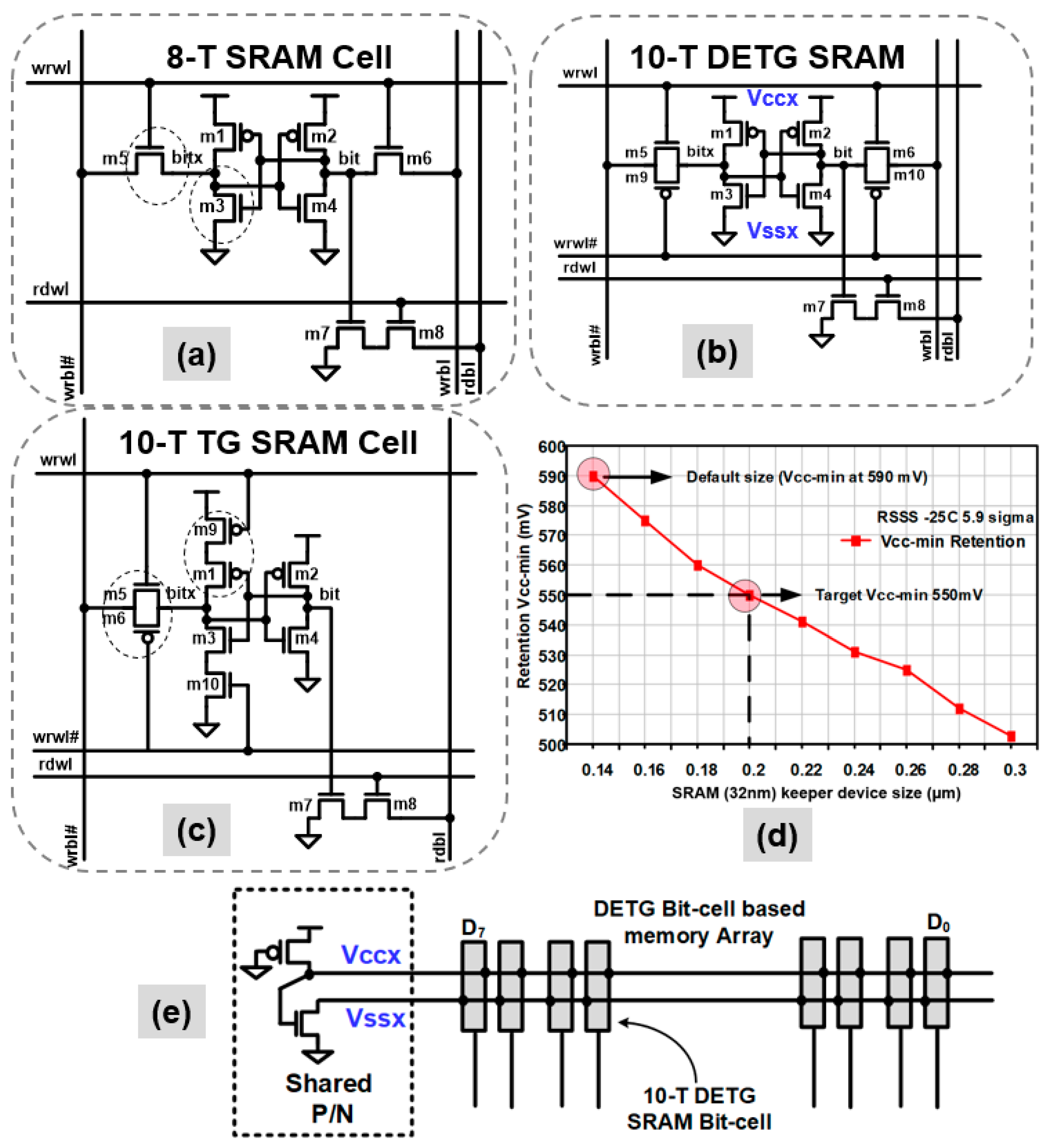
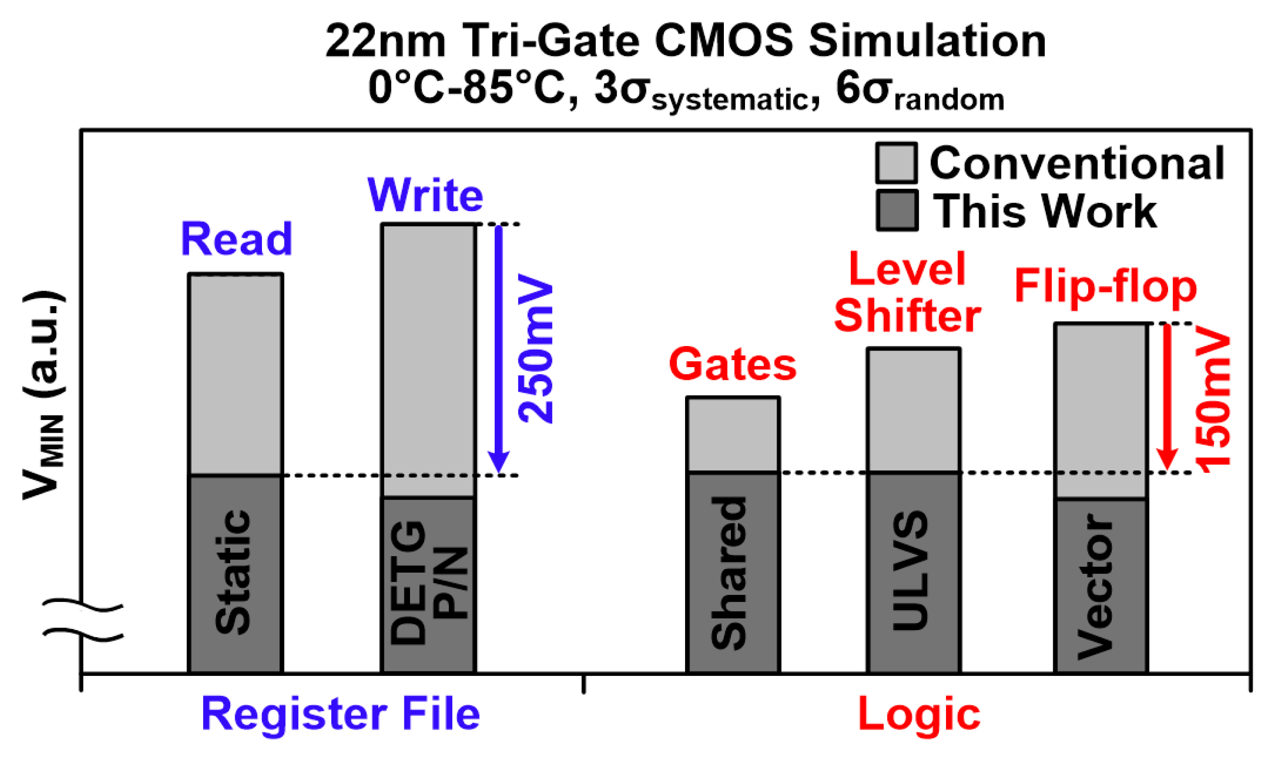
2.1. SRAM Memory and Register File (RF) Optimizations

An 8-T SRAM cell (Figure 2a) is commonly used in single-VDD microprocessor cores, particularly in performance critical low-level caches and multi-ported register-file arrays. The 8-T cell offers fast simultaneous read and write, dual-port capability, and generally lower Vmin than the 6-T cell. With independent read and write ports in the 8-T cell, significantly improved read noise margins can be realized over the traditional 6-T SRAM cell, at an additional area expense. The noise margin improvement is due to the elimination of the read-disturb condition of the internal memory node by the introduction of a separate read port in the SRAM cell. As a result, variability tolerance is greatly enhanced, making it a desirable design choice for ULP SRAM memory operating at lower supply voltages down to NTV and energy-optimum points.
The 8-T bit-cell is still prone to write failures due to write contention between strong PMOS pull-up and a weak NMOS transfer device across PVT variation. This contention becomes worse as VDD is lowered, limiting Vmin. A variation-tolerant dual-ended transmission gate (DETG) cell is implemented on the 22-nm NTV-SIMD register file array by replacing the NMOS transfer devices with full transmission gates (Figure 2b). This design enables a strong “1” and “0” write on both sides of the cross-coupled inverter pair. The DETG cell always has two NMOS or two PMOS devices to write a “1” or “0”, on nodes bit and bitx. This inherent redundancy averages the random variation effect across the transistors, improving both contention and write-completion. Moreover, the cell is symmetric with respect to PMOS and NMOS skew which reduces the effect of systematic variation. DETG cell simulations show 24% improvement in write delay, allowing a 150 mV reduction in write Vmin. However, the DETG cell is contention limited at its write Vmin, which can be reduced by the shared P/N circuits. An always “ON” PMOS and NMOS is shared across the virtual supplies of eight DETG cells (Figure 2e). The shared P/N circuit limits the strength of the cross-coupled inverters across variations reducing write contention by 22%. This circuit optimization results in an additional 125 mV write reduction compared to DETG, enabling an overall 275 mV write Vmin reduction when compared to the 8-T SRAM cell.
Caches in the 32-nm NTV-CPU use a modified, single-ended and fully interruptible 10-T transmission gate (TG) SRAM bit-cell (Figure 2c), which allows for contention-free write operations. This topology enables a 250 mV improvement in write Vmin over an 8-T bit-cell. With this improvement, bit-cell retention now becomes a key VDD limiter. The simulated retention voltage data for the 10-T TG SRAM, as a function of keeper device size (m9, m10) and in the presence of random variations (5.9σ, slow skew, −25 °C) is shown in Figure 2d. Clearly, larger keeper devices lower the retention voltage. The keeper device is increased from 140-nm to 200-nm to realize a 550 mV retention Vmin target. For reliable read operation, bit-lines incorporate a scan-controlled, programmable stacked keeper, which can be configured to three or four PMOS device stacks to reduce read contention and improve read Vmin, across wide operating voltage/frequency range.
To achieve low standby power in the WSN, all on-die memories and caches on the 14-nm NTV-MCU use a custom 8-T (Figure 2a), 0.155-µm2 bit-cell, built using 84-nm gate pitch ultra-low power (ULP) transistors [14]. The 8-T bit-cell provides a well-balanced trade-off in Vmin and area over the 6-T and 10-T SRAM cells. The ULP transistor optimized memory arrays are designed to provide low standby leakage. However, as summarized in Table 2, a 5× performance slowdown is estimated over standard performance (SP) transistor 8T memory at 500 mV, but is still fast enough for edge compute applications. Context-aware power-gating of each 2 KB array is supported for further leakage reduction with no state retention. The ULP array also enables 26× lower leakage (at 500 mV supply) and has a 55% area cost over an SP-based 8T memory array, drawn on a 70 nm gate pitch. The ULP memory leakage scales from 114 pA at 1 V voltage down to 8.28 pA per bit at the retention limit of 308 mV, as measured at room temperature (25 °C).
Process, voltage and temperature (PVT) and aging adaptive on-die boosting of read word-line (RWL) and write word-line (WWL) as a common circuit assist technique for further lowering SRAM Vmin is described in [16,17]. Boosting RWL enables larger read “ON” current without forcing a larger PMOS keeper. Boosting WWL helps write Vmin for two reasons—it improves contention without upsizing NMOS pass device size (or lowering its VTH), and improving write completion by writing a “1” from the other side. At iso-array area, on-die WL boosting achieves twice as much Vmin reduction over bit- cell upsizing [16]. However, word-line boosting requires an integrated charge-pump, or another method for generating a boosted voltage on die.

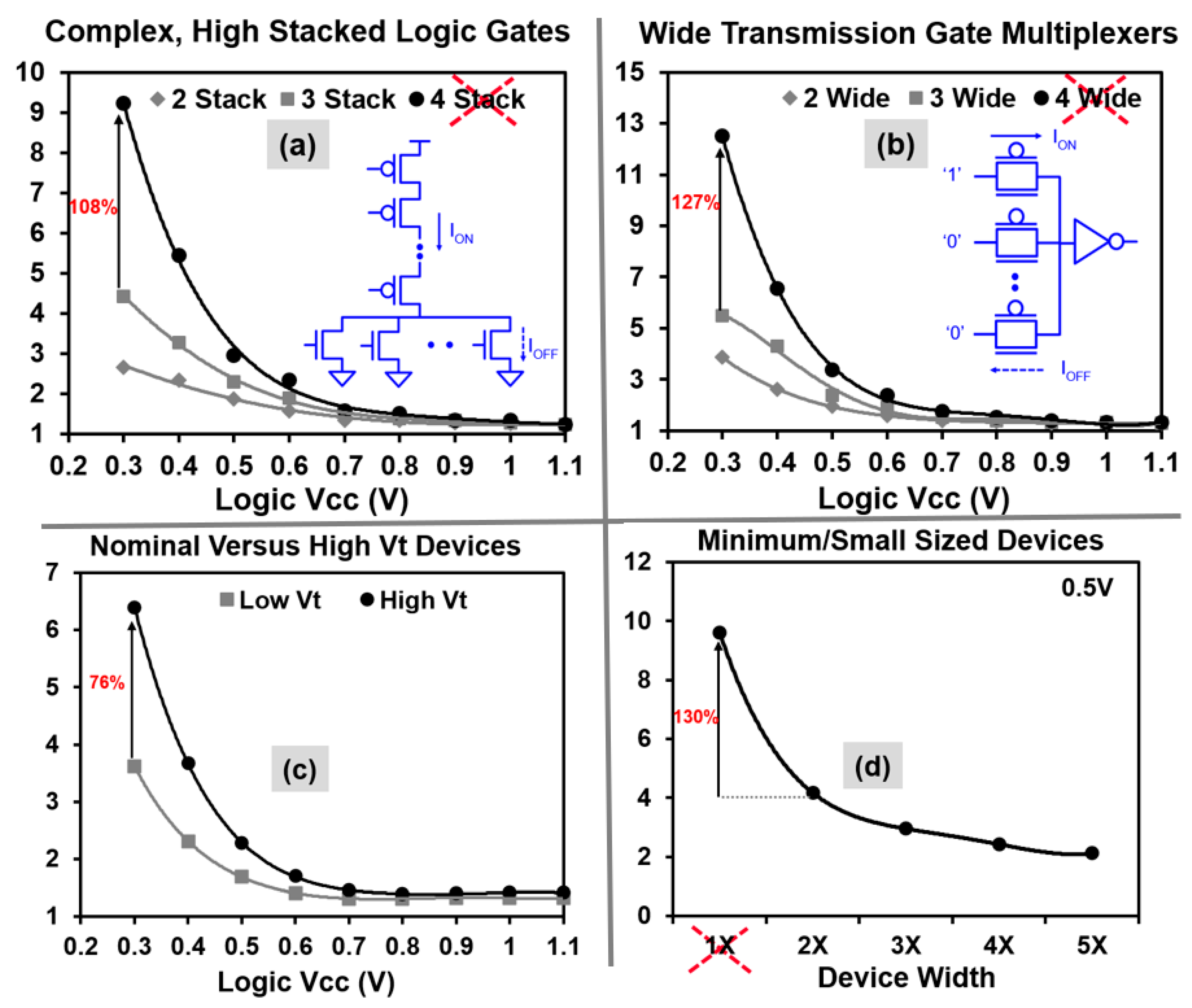
2.2. Combinational Cells Design Criteria

Circuits are optimized for robust and reliable ultra-low voltage operation. A variation-aware pruning is performed on the standard cell library to eliminate the circuits which exhibit DC failures or extreme delay degradation at NTV due to reduced transistor on/off current ratios and increased sensitivity to process variations. Simulated 32-nm normalized gate delays (y-axis), as a function of VDD for logic devices in the presence of random variations (6σ) is presented in Figure 3. Complex logic gates with four or more stacked devices and wide transmission-gate multiplexers with four or more inputs are pruned from the library because they exhibit more than 108% and 127% delay degradation compared to three stack or three-wide multiplexers respectively (Figure 3a,b). Critical timing paths are designed using low VT devices because high VT devices indicate 76% higher delay penalty at 300 mV supply, in the presence of variation (Figure 3c). All minimum-sized gates with transistor widths less than 2× of the process-allowed minimum (ZMIN) are filtered from the library due to 130% higher variation impact (Figure 3d), and the use of single fin-width devices is limited in 22-nm and 14-nm logic design.

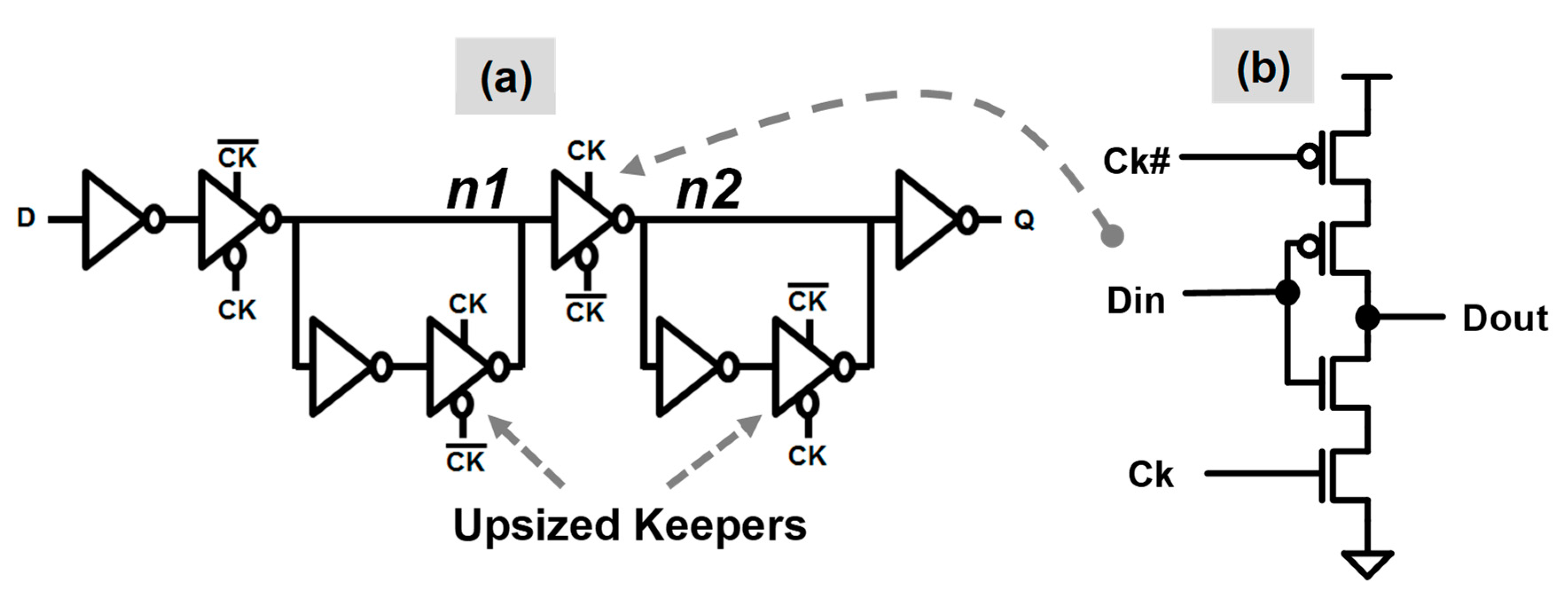
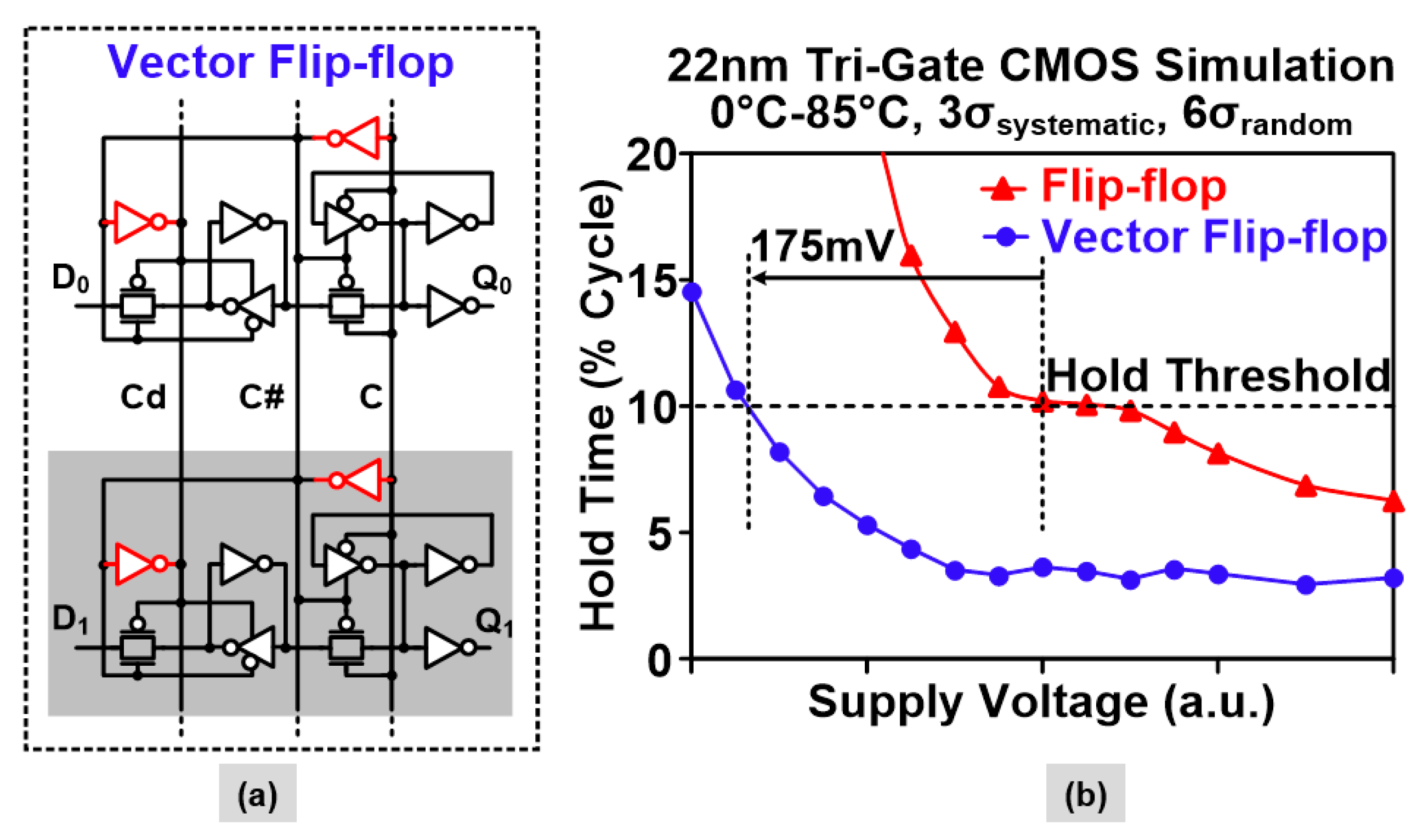
2.3. Sequential Circuit Optimizations

At lower supply voltages, degradation in transistor Ion/Ioff ratio, random and systematic process variations, affect the stability of storage nodes in flip-flops. Conventional transmission gate based master-slave flip-flop circuits typically have weak keepers for state nodes and larger transmission gates. During the state retention phase, the on-current of weak keeper contends with the off-current of the strong transmission gate affecting state node stability. Additionally, charge-sharing between the internal master and slave nodes (write-back glitch) can result in state bit-flip due to reduced noise margins at low VDD. The NTV-CPU employs custom sequential circuits to ensure robust operation at lower voltages under process variations. A clocked CMOS-style flip-flop design (Figure 4) replaces master and slave transmission gates with clocked inverters, thereby eliminating the risk of data write-back through the pass gates. In addition, keepers are upsized to improve state node retention and are made fully interruptible to avoid contention during the write phase of the clock, thus improving Vmin.
Clock edges also degrade severely at low voltages, since local clock drivers inside flip-flops are small (ZMIN) and prone to process variations. This can cause hold-time degradations and min-delay failures. The NTV-SIMD engine employs vector flip-flops, where the clock outputs of local drivers are shared across the flip-flops. As shown in Figure 5a, the drivers on nodes C, C# and Cd are shared across multiple flip-flops. This helps average the impact of device parameter variations. In addition, vector flip-flops enable lower clock power since they present a reduced input capacitance to the clock tree drivers. Under worst-case variation, if one of the local clock inverters becomes weak, the other shared clock inverter will compensate for the reduced drive strength. Vector flip-flop simulations (22-nm) across two adjacent cells with shared local min-sized clock inverters (Figure 5b) show better hold time violations at NTV and improved hold time margins by 175 mV. Stacked min-delay buffers limit variation-induced transistor speed up, further improving hold time margins at NTV by 7–30%.

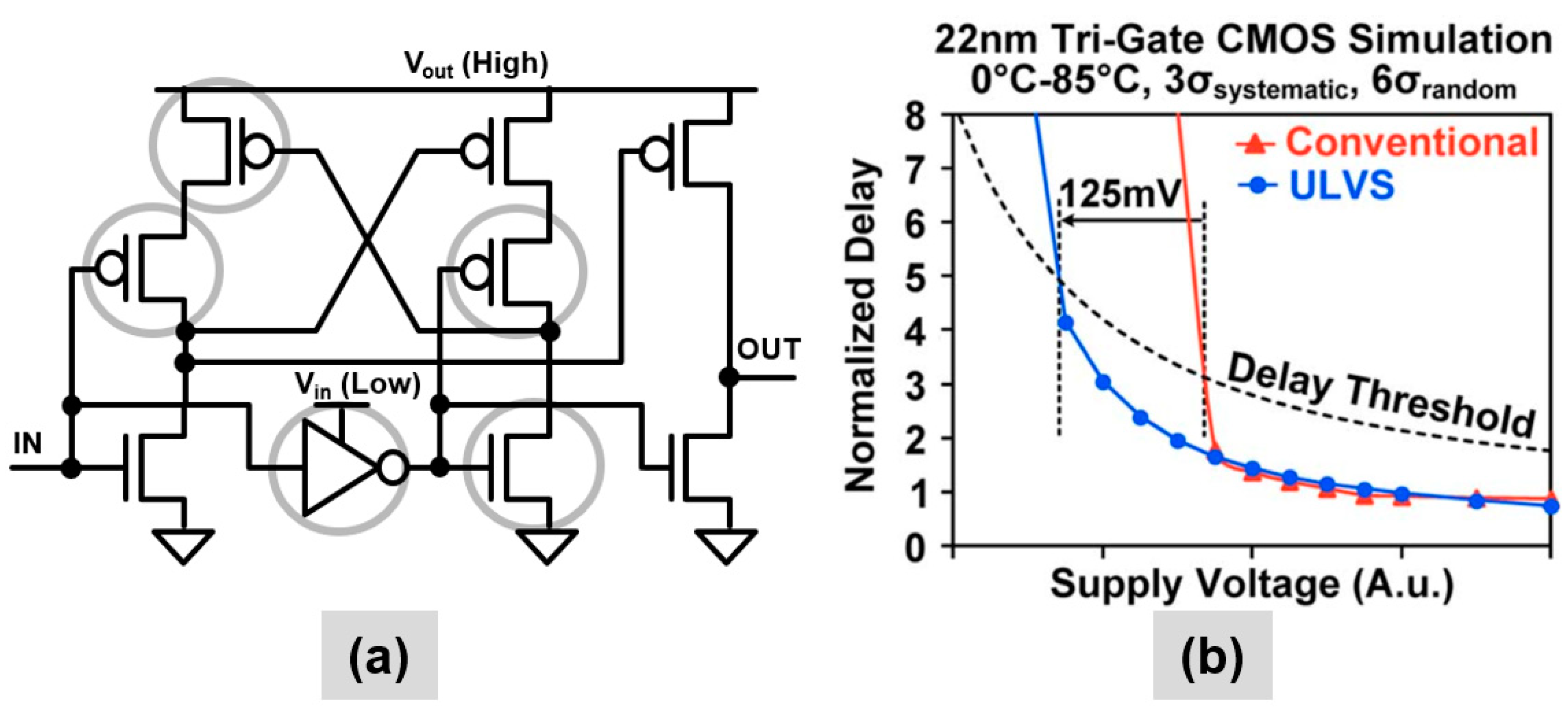
2.4. Level Shifter Circuit Optimizations

NTV designs, operating at low supply voltages require level shifters to communicate with circuits at the higher voltages (e.g., I/O). Similar to register file writes, conventional CVSL level shifters are inherently contention circuits. The need for wide range, ultra-low voltage level shifter to a high supply voltage further exacerbates this contention. The ultra-low voltage split-output, or ULVS, level shifter decouples the CVSL stage from the output driver stage and interrupts the contention devices, thus improving Vmin by 125 mV (Figure 6). Full interruption of contention devices occurs for voltages Vin ≥ Vout, while for voltages Vin < Vout the contention devices are only partially interrupted, but still is beneficial at low voltages. For equal fan-in and fan-out, the ULVS level shifter weakens contention devices, thereby reducing power by 25% to 32%.
Figure 7 summarizes improvements achieved from applying multiple circuit techniques for both the register file and logic circuits across 0–85 °C in the 22-nm SIMD engine. The static register file read circuits and shared P/N DETG write SRAM bit-cells improve overall register file Vmin by 250 mV. Shared gates, ULVS level shifters, and vector flip-flops improve overall logic Vmin by 150 mV.

3. Architecture Driven NTV Resilient NoC Fabrics

Architectural techniques can help regain some of the performance loss from engaging aggressive VDD reduction. The limits to NTC-based parallelism to reclaim performance have been discussed in [18]. Dynamic adaptation techniques have been shown to monitor the available timing margin and guard bands in the design and dynamically modulate the voltage/frequency (V/F), thus preventing occurrence of timing errors [19]. Architecture-assisted resilient techniques, on the other hand, are more aggressive with the V/F push. In this case, the errors are allowed to happen, they are detected and then corrected using appropriate replay mechanisms.
Replica path-based methods such as tunable replica circuits (TRC) have been proposed [20] for error detection in flip-flop based static CMOS logic blocks. In this approach, a set of replica circuits are calibrated to match the critical path pipeline stage delay and timing errors are detected by double-sampling the TRC outputs. The key requirement is that the TRC must always fail before the critical path fails. The TRC is an area-efficient and non-intrusive technique, but it cannot leverage the probabilities of critical path activation, multiple simultaneous switching at inputs of complex gates, or worst case coupling from adjacent signal lines. An alternative in-situ approach for timing error detection uses error detection sequentials (EDS) in the critical paths of the pipeline stage. Timing errors are detected by a double-sampling mechanism using a flip-flop and a latch (Figure 8b) [21]. Errors are corrected by performing a replay operation at higher V or lower F. The V/F can also be adapted by monitoring the error rate and accounting for error recovery overheads.
NoCs have rapidly become the accepted method for connecting a large number of on-chip components. Packet-switched routers are key building blocks of NoCs [13]. Margins for operating V/F used to guarantee error-free operation limit achievable energy efficiency and performance at VOPT. While error-correction codes (ECC) have been previously used to mitigate transient failures in routers [22], the associated performance and energy overheads can be significant for detection and correction of multi-bit failures. Timing error detection using EDS has been used for processor pipelines with minimal overhead [21]. An NTV router, designed in a 22-nm node and enhanced with EDS and a FLIT replay scheme, provides resilience to multi-bit timing failures for on-die communication. The goal is to evaluate the performance and energy benefits of single-error correction double-error detection (SECDED) ECC method over an EDS-based approach, from nominal VDD down to NTV.

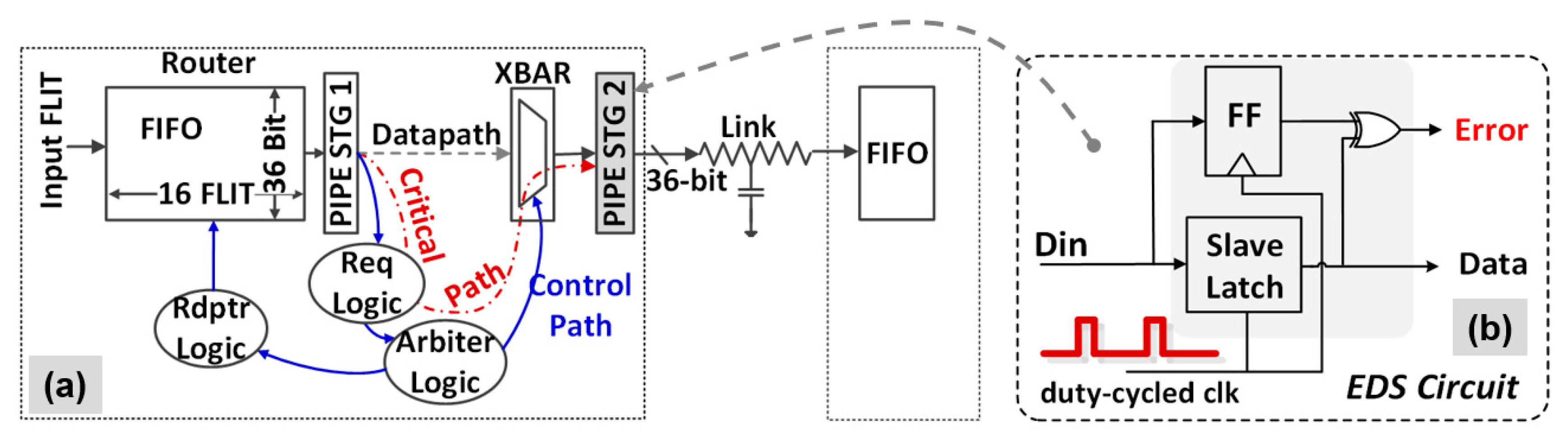
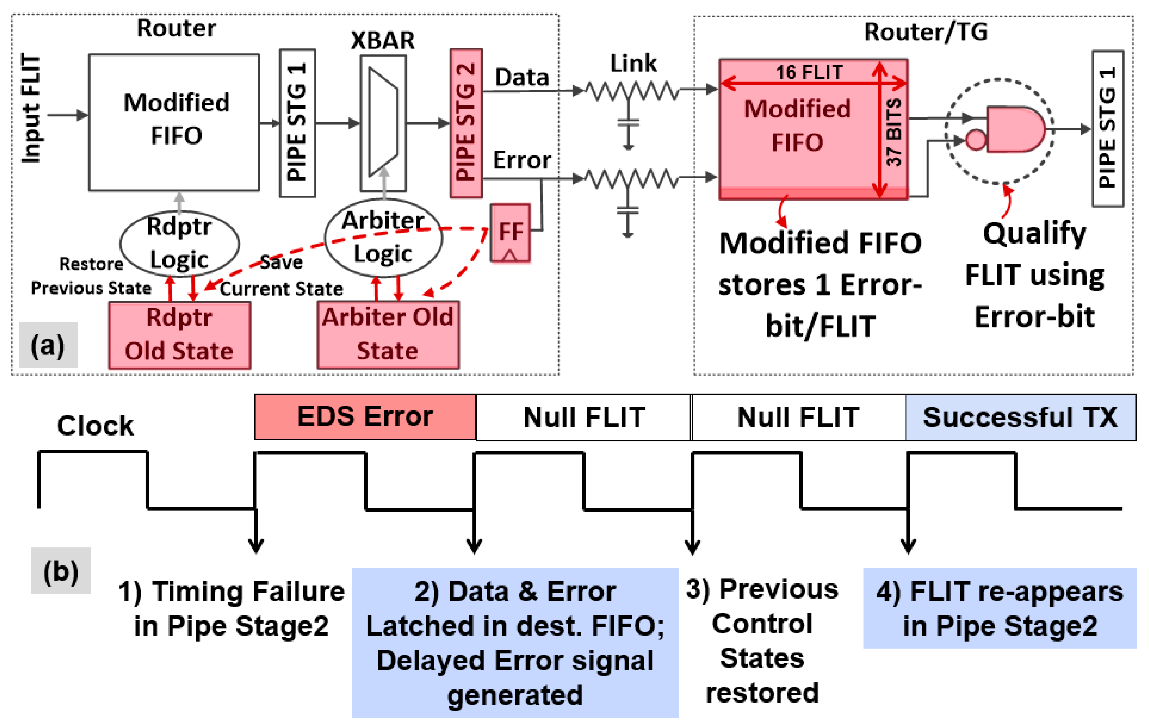
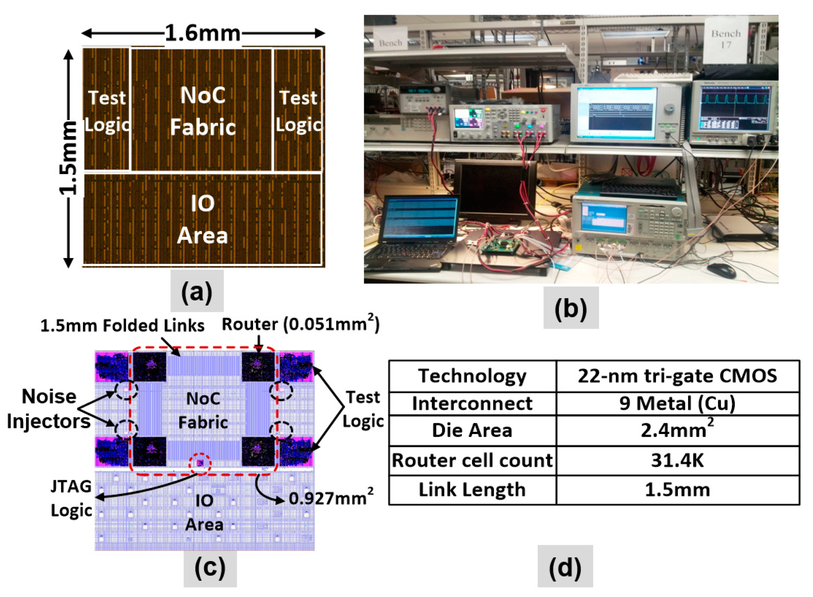
Resilient Router Architecture and Design

The 6-port packet-switched router in the 2 × 2 2-D mesh NoC fabric communicates with the traffic generator (TG) via two local ports and with neighboring routers using four bidirectional, 36-bit 1.5 mm long on-die links (Figure 1c). Inbound router FLITs are buffered in a 16-entry 36-bit wide FIFO (Figure 8a). The most critical timing path in the router consists of request generation, lane and port arbitration, FIFO read, followed by a fully non-blocking crossbar (XBAR) traversal. Any failure in this timing path is detected by the EDS circuit (Figure 8b) embedded in the output pipe stage (STG 2). The two-cycle EDS enhanced router can be run in two modes, with and without error detection. The TG contains SECDED logic which appends or retrieves nine ECC bits from a packet’s tail FLIT, thus allowing end-to-end detection and correction of errors in the payload. A programmable noise injector [21] is introduced at each node on VNoC supply to induce noise events during packet transmission.
The router control logic recovers from timing failures by saving critical states for the last two FLIT transmissions (Figure 9a). In the event of a timing failure, the Error signal generated by the EDS circuit in STG 2 is captured along with the erroneous FLIT in the recipient’s FIFO, modified to accommodate an additional error bit as shown. Forward error correction is achieved by qualifying the FIFO output with the Error flag. In the router with the timing failure, the Error signal is latched to mitigate metastability. This synchronized Error flag is then used to roll-back the arbiters and FIFO read pointers to the previous functionally correct state. The current FLIT is again forwarded as part of replay. Error synchronization and roll-back incur two clock cycles of delay between an error event and successful recovery (Figure 9b). To avoid min-delay failures at STG 2, a clock with scan-tunable duty cycle control is implemented for the EDS latches. Additional min-delay buffers are inserted in the crossbar data path for added hold margin at a 2.4% area cost. In addition, the resilient router incurs the following overheads: (a) About 2.5% of router sequentials are converted to EDS; (b) Enabling replay causes a 10.5% increase in sequential count with 1.6% area overhead; and (c) The power overhead for the entire router is 8.7% with a 2.8% area cost.

4. Designing for Wide-Dynamic Range: Tools, Flows and Methodologies

Device optimizations need to work in concert with automated CAD design flows for optimal results. The 14-nm NTV-WSN design uses HP, standard-performance (SP), ULP, and thick-gate (TG)—all four transistor families in 14-nm second-generation tri-gate SoC platform technology [14]. To minimize variation induced skews, the clock distribution is completely designed using HP devices. The lower threshold voltage (VT) of the HP devices allows improved delay predictability on the clock paths at NTV. SP devices are used for 100% of logic cells to achieve sufficient speeds during active mode of operation, with memory using ULP transistors for low standby power. The bidirectional CMOS IO circuits are designed using high voltage (1.8 V) TG transistors.
The optimized cell library for wide operational range is characterized at 0.5 V, 0.75 V and 1.05 V VDD corners for design synthesis and timing convergence and are optimized for robust and reliable ultra-low voltage operation. Statistical static timing analysis (SSTA) is employed—a method which replaces the normal deterministic timing of gates and interconnects with probability distributions and provides a distribution of possible circuit outcomes [23,24]. As discussed in Section 2.2, variation-aware SSTA study is performed on the standard cell library to eliminate the circuits which exhibit DC failures or extreme delay degradation due to reduced transistor on/off current ratios and increased sensitivity to process variations. As a result, the standard cell library was conservatively constrained for use in the NTV optimized designs.
Achieving the performance targets across the entire voltage range is challenging since critical path characteristics change considerably due to non-linear scaling of device delay and a disproportionate scaling of device versus interconnect (wire) delay. It is critical to identify an optimal design point such that the targeted power and performance are achieved at a given corner without a significant compromise at the other corner. Synthesis corner evaluations for the NTV-CPU (Figure 10a) suggest that 0.5 V, 80 MHz synthesis achieves the target frequency at both 0.5 V (80 MHz) and 1.05 V (650 MHz). In comparison, it is observed that 1.05 V synthesis does not sufficiently size up the device dominated data paths which become critical at lower voltages, resulting in 40% lower performance at 0.5 V. Although 1.05 V synthesis achieves lower leakage and better design area, the 0.5 V corner was selected for final design synthesis of the NTV prototypes, considering its low voltage performance benefits and promise for wide operational range. Performance, area and power metrics at the two extreme design corners in a 32-nm node are presented in Figure 10b. For subsequent NTV prototypes, a multi-corner design performance verification (PV) methodology that simultaneously co-optimizes timing slack across all the three performance corners was developed. This PV approach ensures that performance targets are met across the wide voltage operational range. The method accounts for non-linear scaling of device delays in the critical path versus interconnect delay scaling across wide VDD. At low voltages, severe effects of process variations result in path delay uncertainties and may cause setup (max) or hold (min) violations. Setup violations can be corrected by frequency binning. However, hold violations can cause critical functional failures. The design timing convergence methodology is enhanced to consider the effect of random variations and provide enough variation-aware hold margin guard-bands for robust NTV operation.

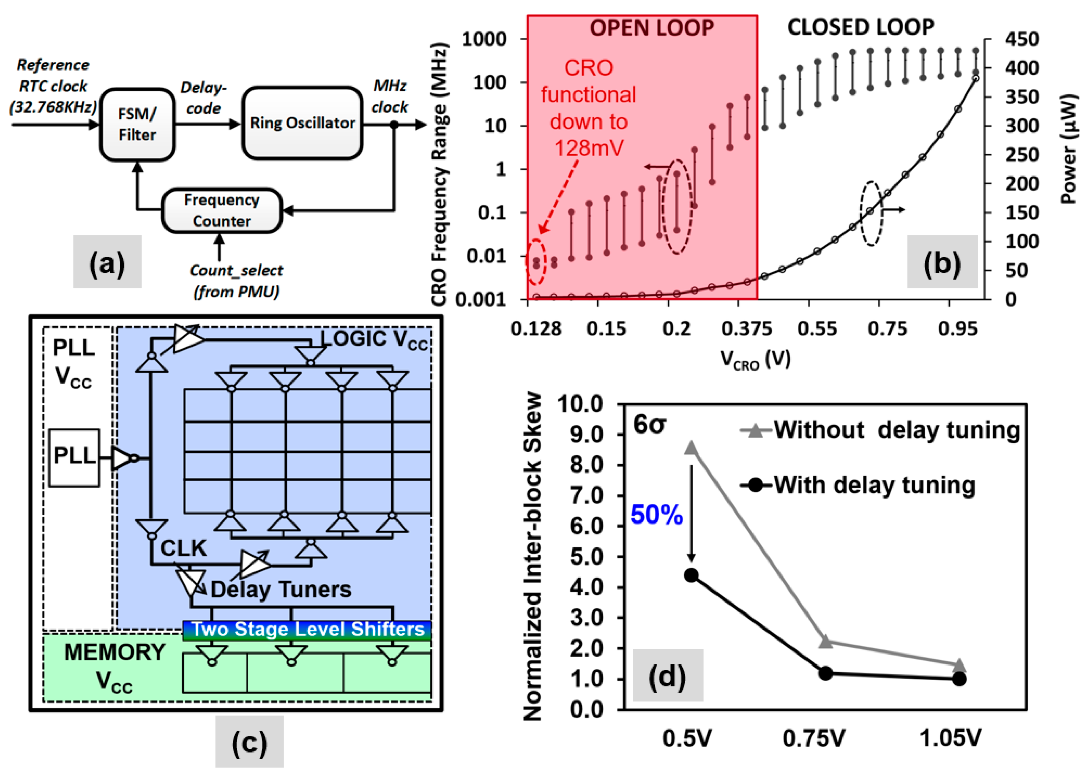
NTV Clocking Architecture

A calibrated ring oscillator (CRO) serves as a low-power on-chip high-frequency (MHz) clock source for the 14-nm NTV-MCU. The CRO is a frequency-locked loop (Figure 11a) that uses an RTC as a reference to generate a MHz clock output. Internally, the CRO tracks the frequency of oscillation from a ring oscillator and generates a delay code that adjusts the oscillation frequency to closely match the target frequency based on the reference clock. The CRO can operate in (1) closed-loop mode, where it accurately tracks the target frequency, as well as in (2) open loop mode at ultralow voltages, producing clock with tens of KHz frequency, enough for always-on (AON) sensing operation on the MCU. Silicon characterization data for the CRO is presented in Figure 11b. The on-die CRO locks to a wide range of target frequencies from 1 V down to 0.4 V. The CRO dissipates 60 µW (450 mV) while generating a 16 MHz output to clock the MCU at VOPT. In open-loop condition, the CRO is functional down to a deep sub-threshold voltage of 128 mV, dissipating 3.8 µW, while generating a 7-kHz clock output. The CRO achieves a measured clock period jitter of 4.6 ps at 400-MHz operation.
The low-VDD global clock distribution network on the NTV-CPU (Figure 11c) is designed with low-VT devices to minimize clock skew across logic and memory voltage domain crossings, across the entire operating voltage range, and considers the effect of random variations. The clock tree incorporates two-stage level shifters and programmable delay buffers in the clock path. The level shifters in the clock path track the delay in the data-path level shifters. In addition, programmable lookup table based delay buffers can be tuned to compensate for any inter-block skew variations. SSTA (6σ) variation analysis shows 50% skew reduction at 0.5 V from clock delay tuning (Figure 11d).

5. Key Results from Experimental NTV Prototypes

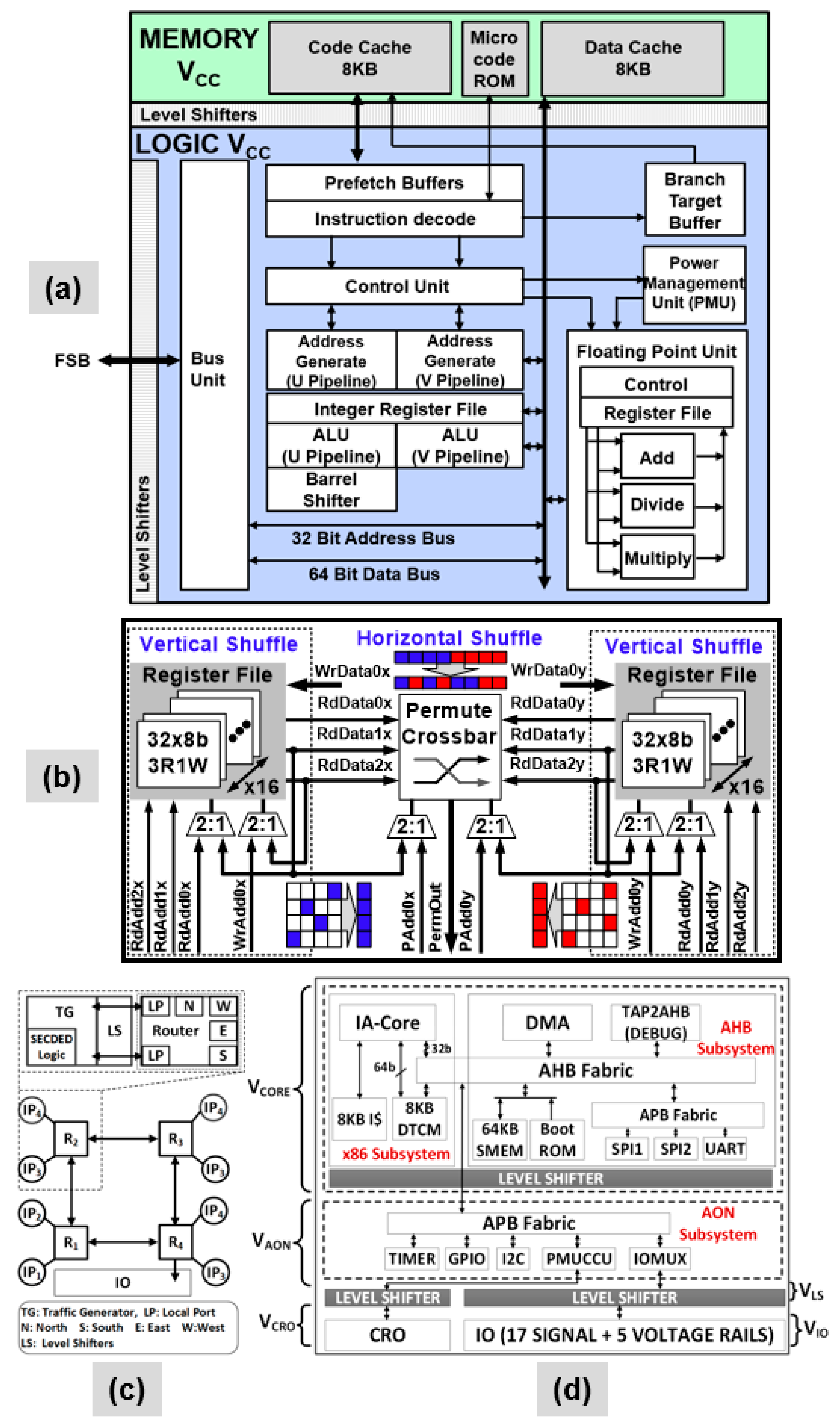
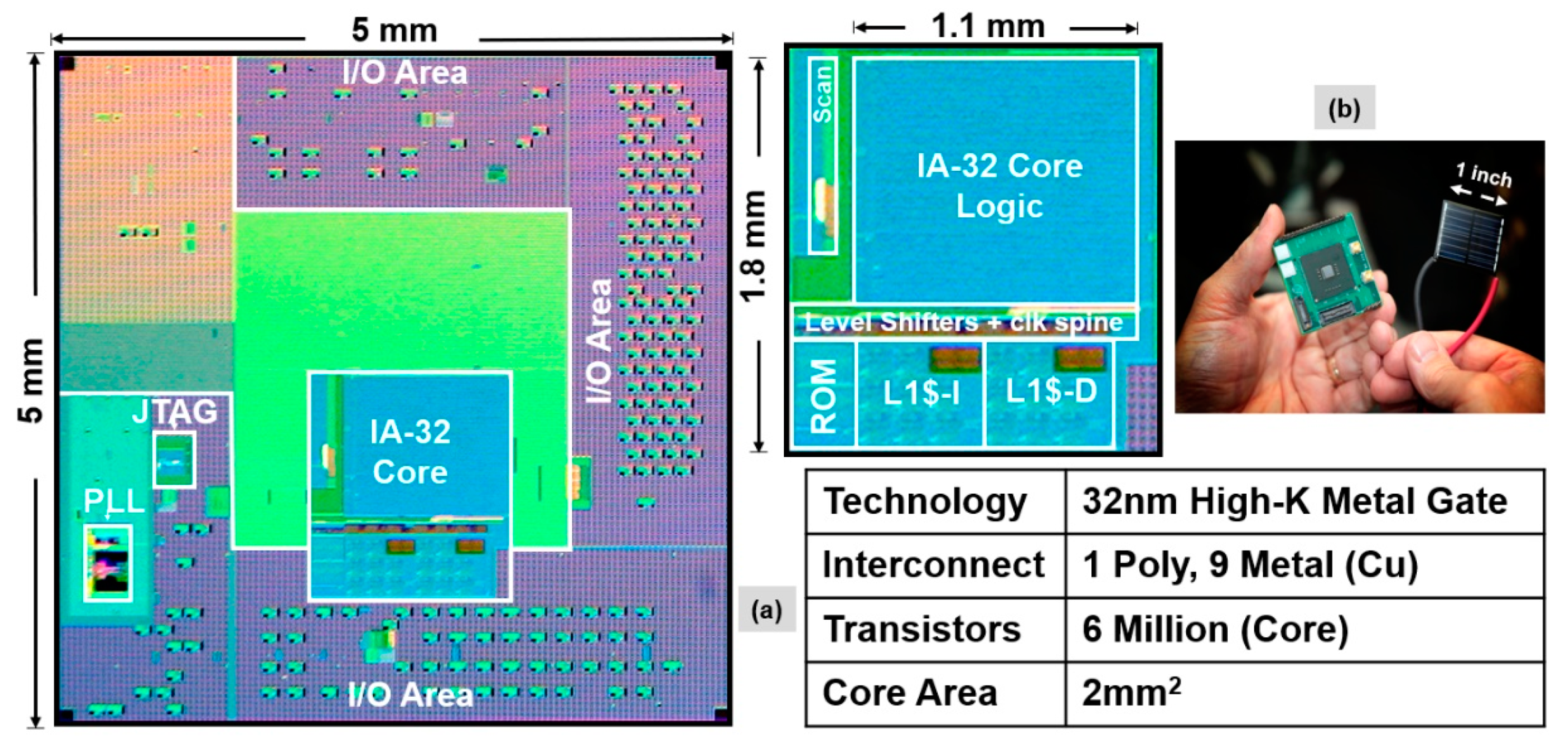
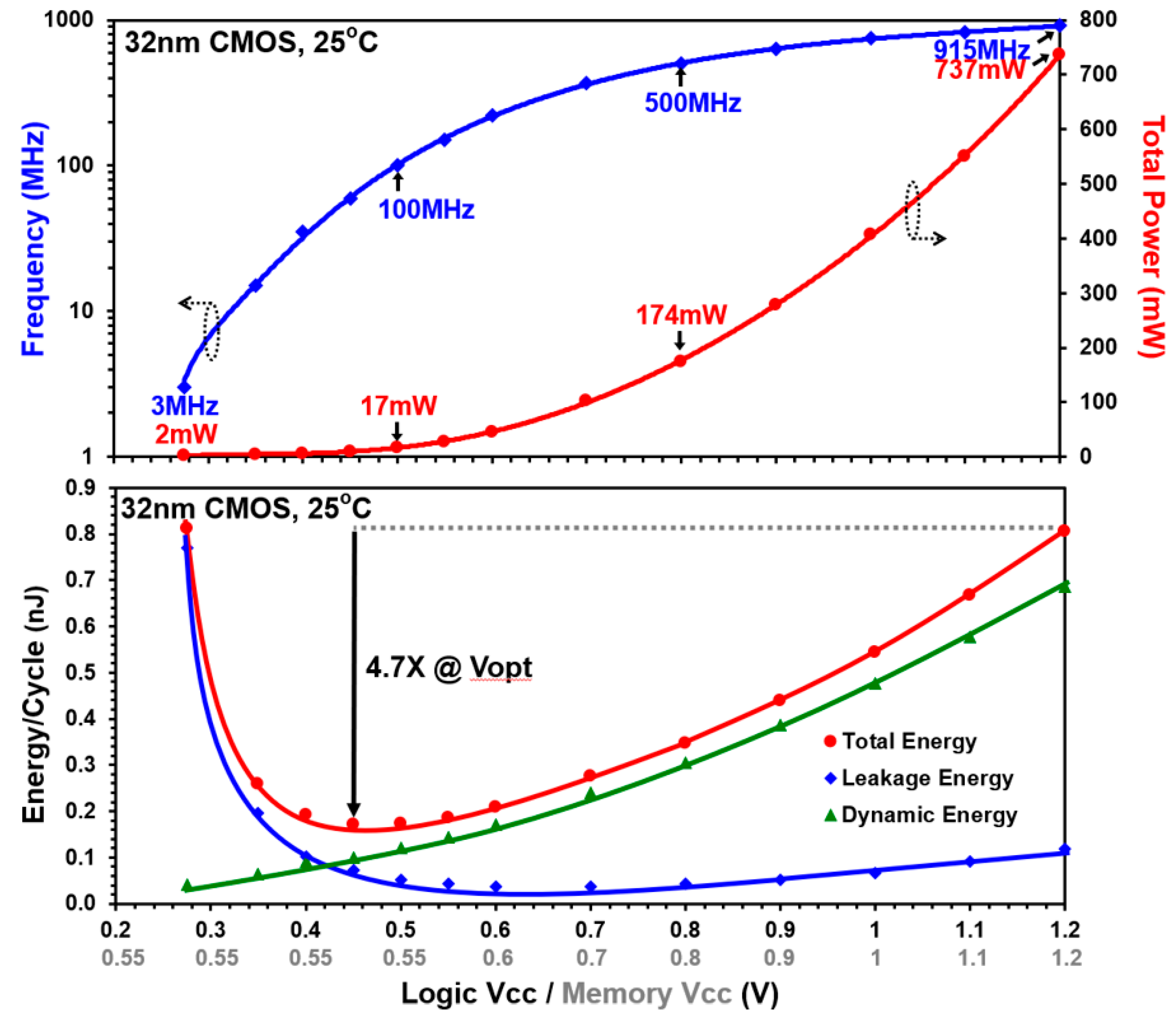
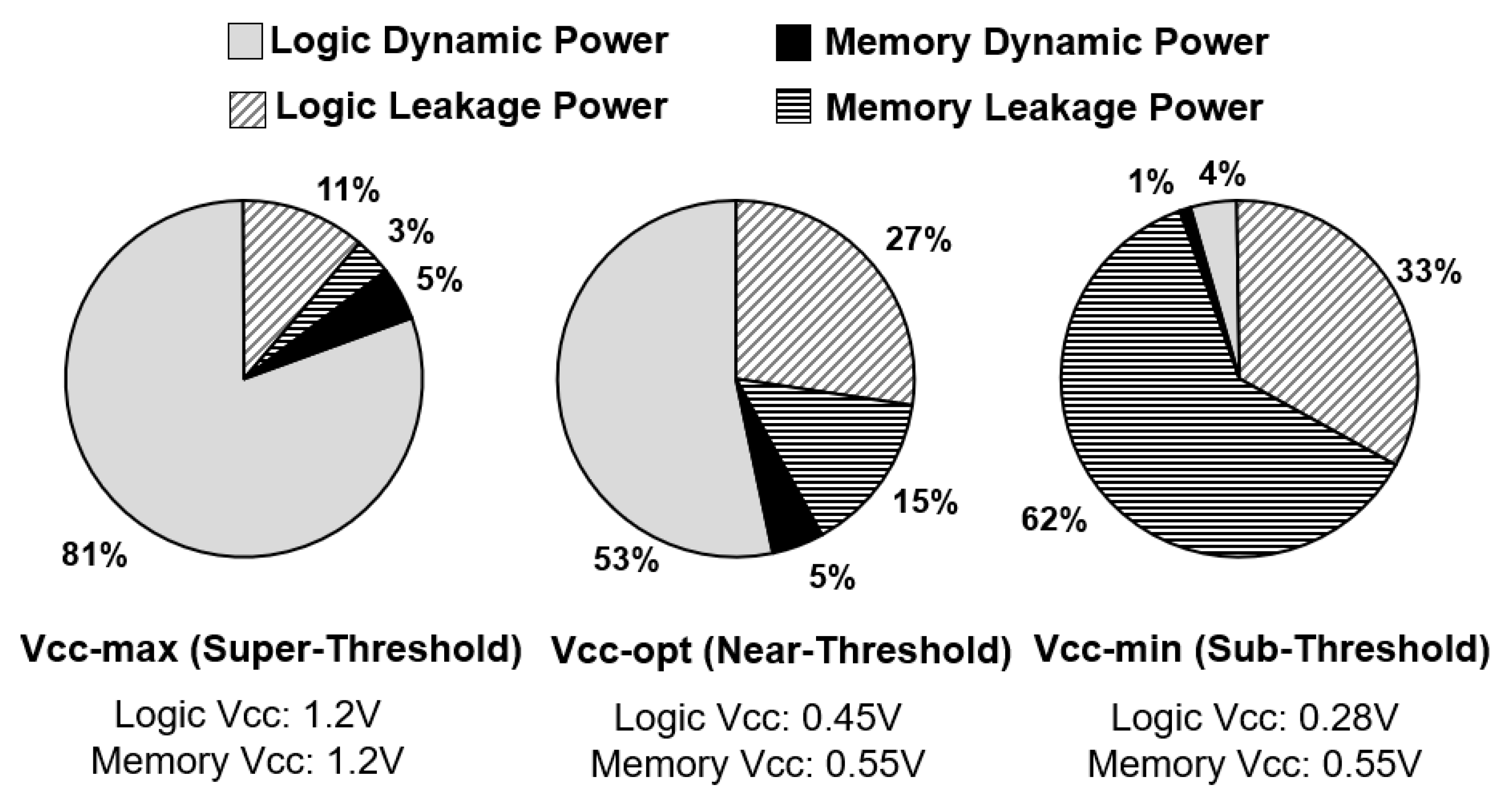
5.1. NTV-CPU Results

The NTV Processor is fabricated in a 32-nm CMOS process technology with nine layers of copper interconnect. Figure 12a shows the IA-32 die and core micrographs with a core area of 2 mm2. Figure 12b shows the packaged IA processor and the solar cell (1 square inch area) used to power the core. The IA core is operational over a wide voltage range from 280 mV to 1.2 V. Figure 13 shows the measured total core power and maximum operational frequency (Fmax) across the voltage range, measured while running the Pentium Built-In Self-Test (BIST) in a continuous loop mode. Starting at 1.2 V and 915 MHz, core voltage and performance scales down to 280 mV and 3 MHz, reducing total power consumption from 737 mW to a mere 2 mW. With a dual-VDD design, memories stay at its measured VDD-min of 0.55 V while allowing IA core logic to scale further down till 280 mV.
Figure 13 also plots the measured total energy per cycle across the wide voltage range along with its dynamic and leakage components. Minimum energy operation is achieved at NTV, with the total energy reaching minima of 170 pJ/cycle at 450 mV (VOPT), demonstrating 4.7× improvement in energy efficiency compared to the VDD-max (1.2V) corner.
The pie-charts in Figure 14 shows a total core power breakup across super-threshold, near-threshold and sub-threshold regions. The contribution of logic dynamic power reduces drastically from 81% at VDD-max to only 4% at VDD-min (280 mV). Chip leakage power contribution as a proportion of total power starts increasing in the near-threshold voltage region and accounts for 42% of the total core power at VDD-opt. At VDD-min point, memories continue to stay at a higher VDD than logic (550 mV), thus contributing 63% of the total core power.

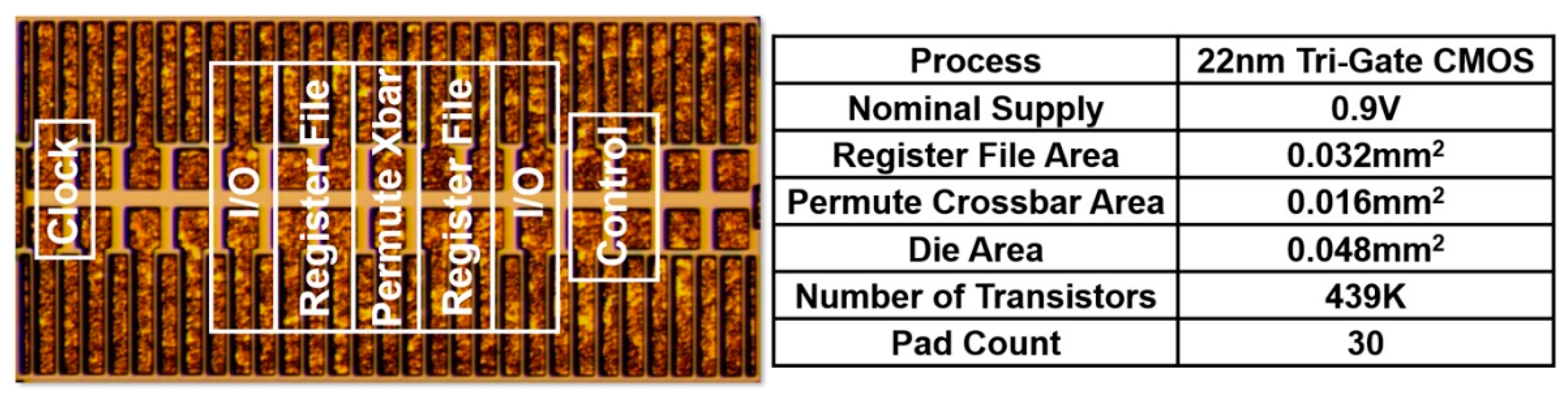
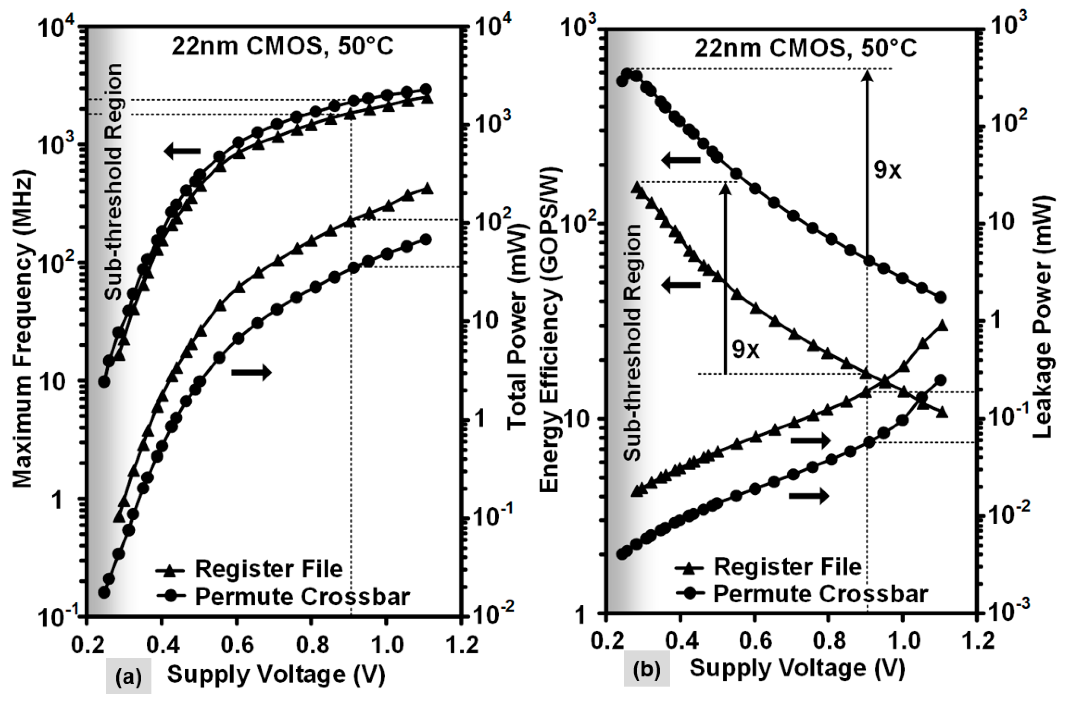
5.2. NTV-SIMD Engine Results

The SIMD permutation engine operates at a nominal supply voltage of 0.9 V and is implemented in a 22-nm tri-gate bulk CMOS technology featuring high-k metal-gate transistors and strained silicon technology. Figure 15 shows the die micrograph of the chip with a total compute die area of 0.048 mm2. The permutation engine with 2-dimensional shuffle results in 36% to 63% fewer register file reads, writes, and permutes compared to a conventional 256b shuffle-based implementation. The SIMD engine contains 439,000 transistors.
Frequency and power measurements for the SIMD engine components are presented in Figure 16, obtained by sweeping the supply voltage from 280 mV to 1.1 V in a temperature-stabilized environment of 50 °C. Chip measurements show that the register file and crossbar operate from 3 GHz (1.1 V) down to 10 MHz (280 mV). The register file dissipates 227 mW (1.1 V) and 108 µW (280 mV) respectively, while the permute crossbar consumes 69 mW–19 µW over the same VDD range. The maximum energy efficiency of 154 GOPS/W (1 OP = three 256b reads and one 256b write) is obtained at a supply voltage of 280 mV (VOPT) and is 9× higher than the efficiency at nominal voltage. The 256b byte-wise any-to-any permute crossbar executes horizontal shuffle operations down to supply voltages of 240 mV. Peak energy efficiency of 585 GOPS/W (1 OP = one 32-way 256b permutation) is achieved at a supply voltage of 260 mV, also with 9× better energy efficiency.

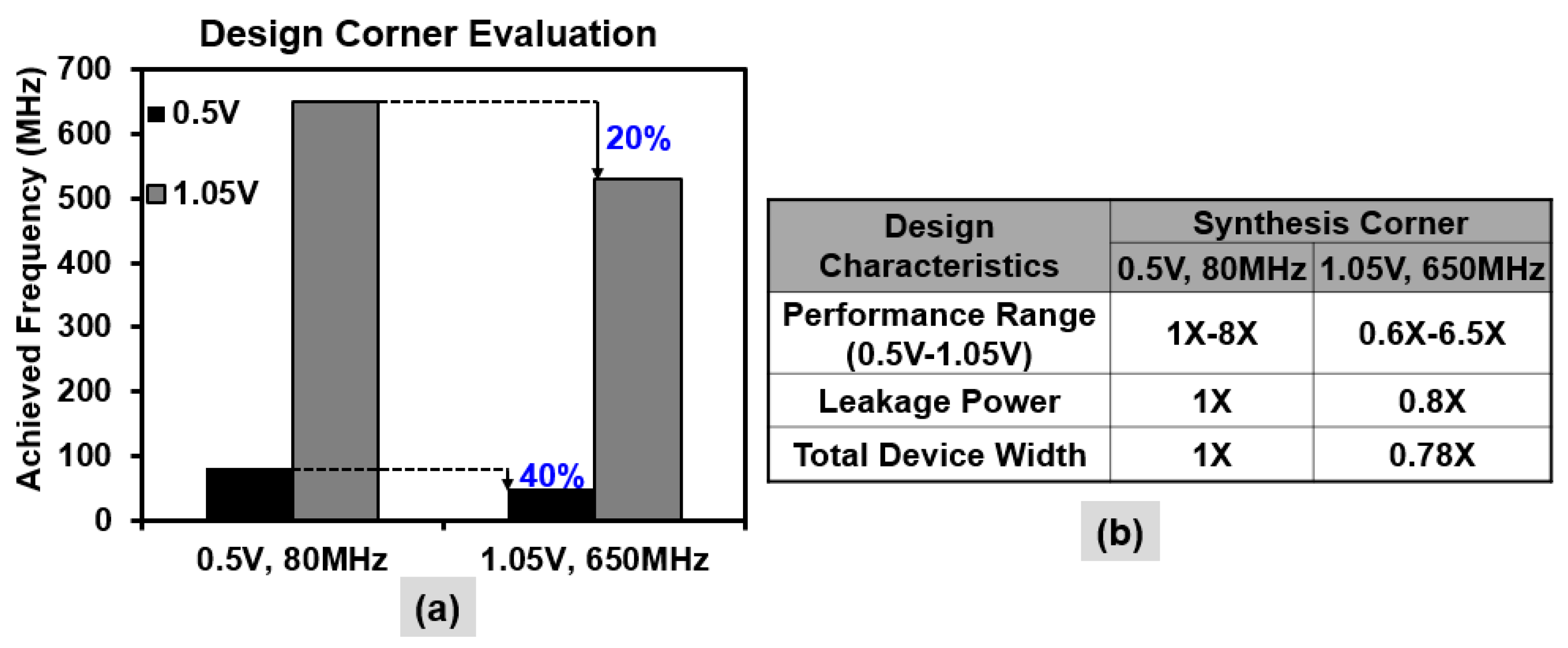
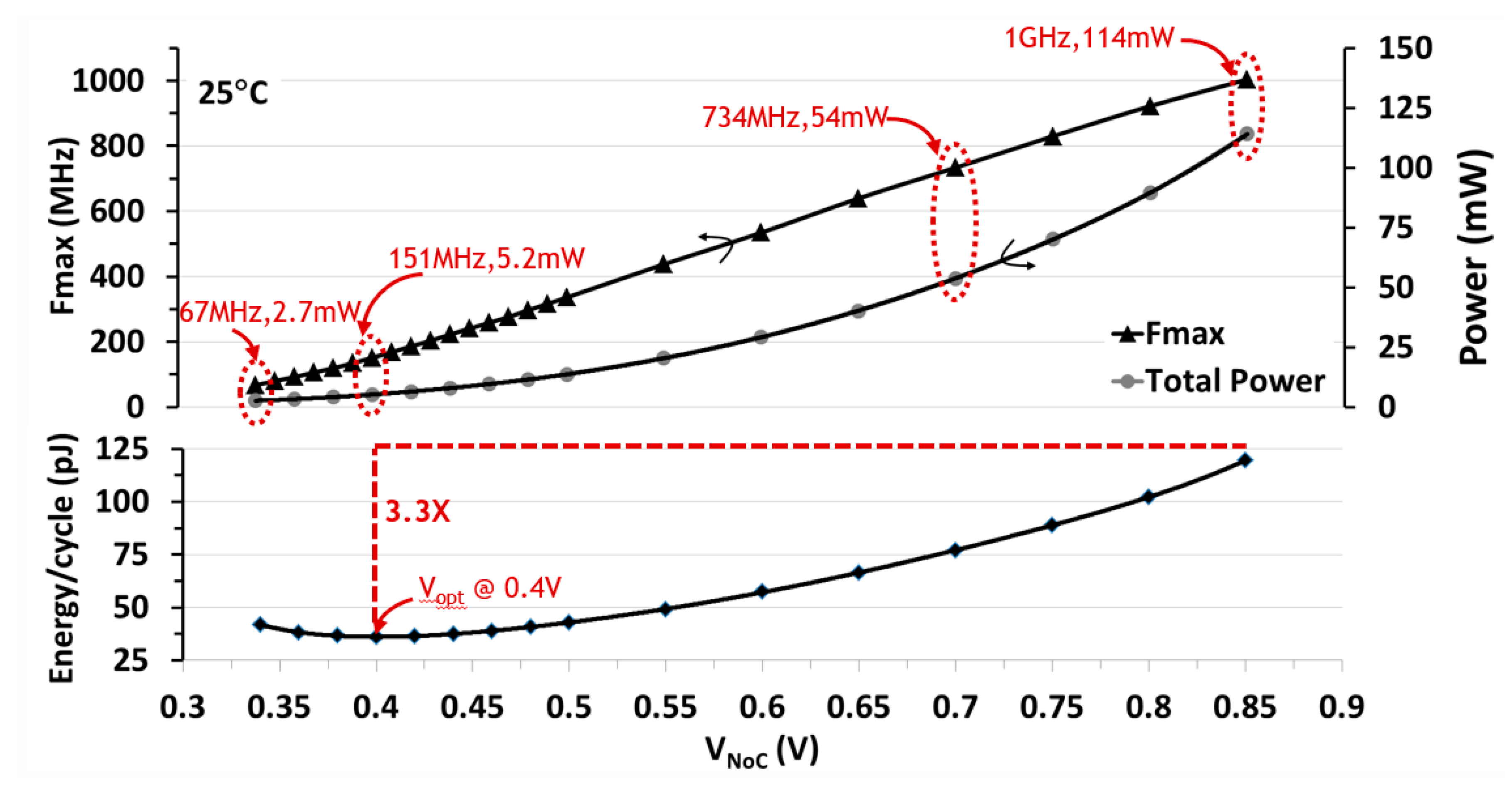
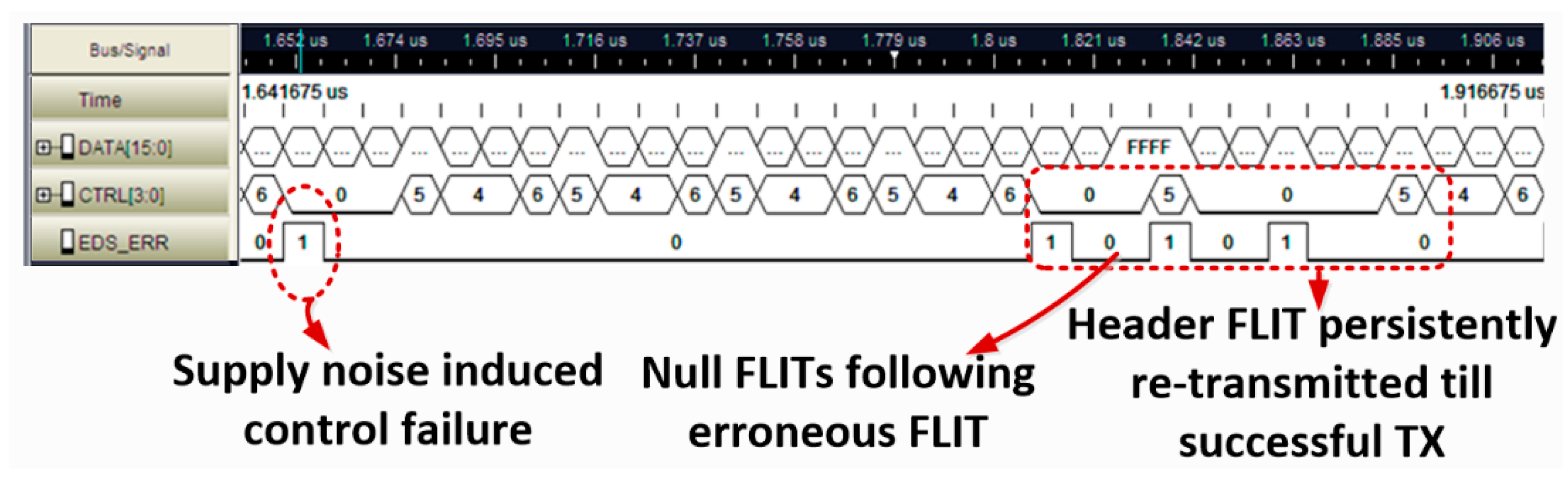
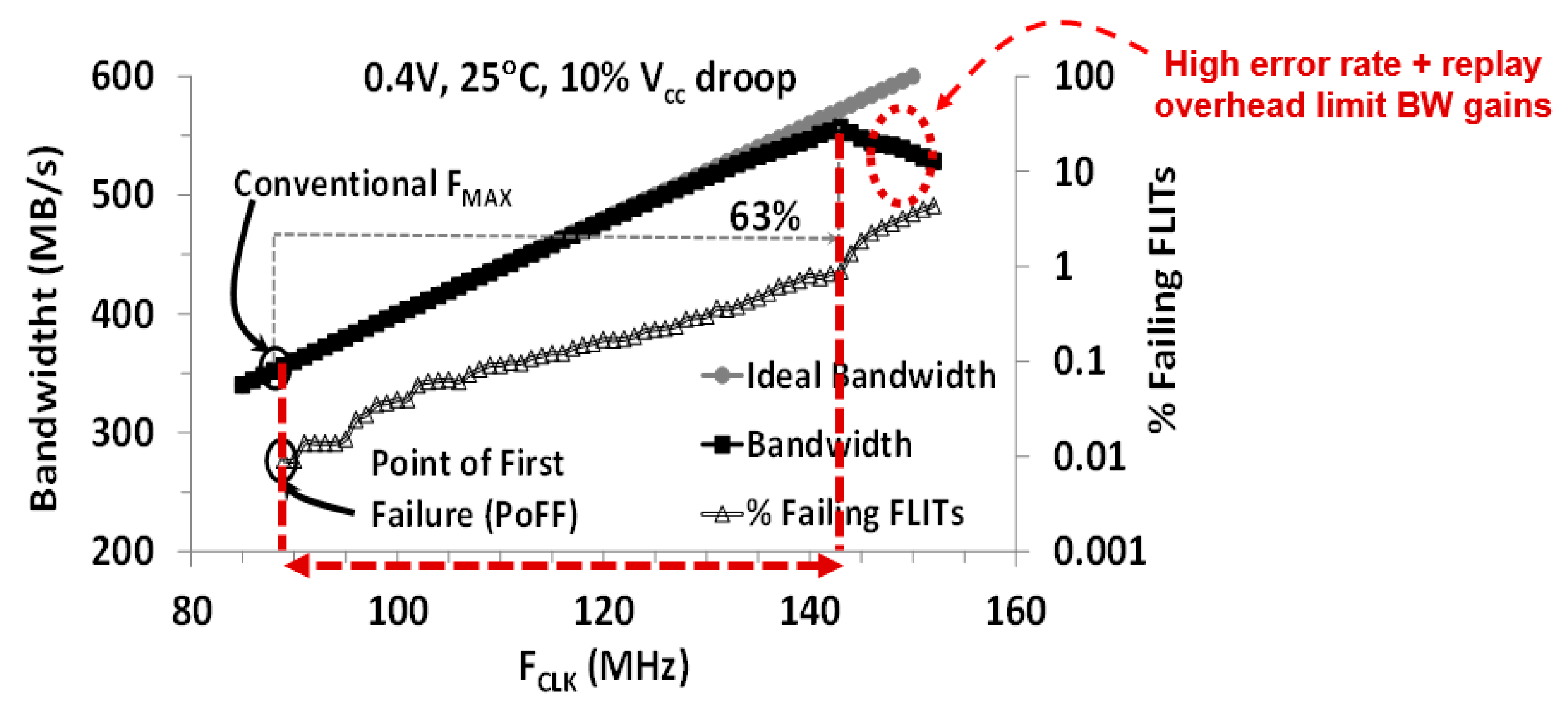
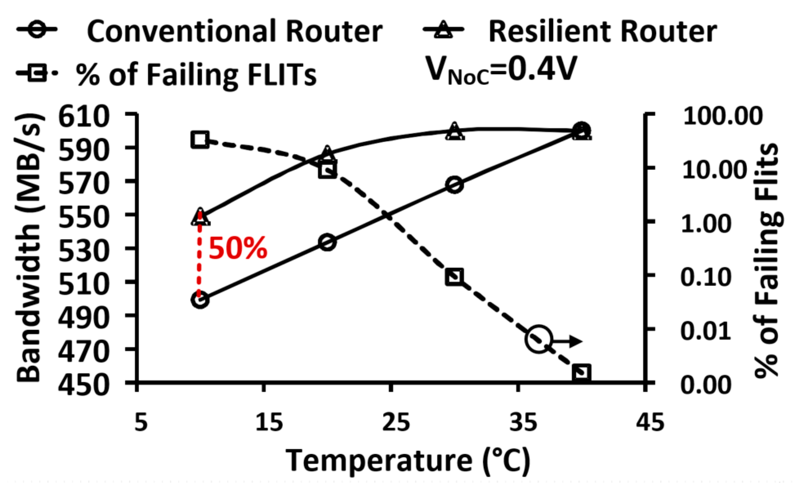
5.3. NTV-NoC Measurement Results and Learnings

The 2 × 2 2-D mesh-based resilient NoC prototype is fabricated in a 22 nm, 9-metal layer technology. Each router port features bidirectional, 36-bit wide, 1.5 mm long on-die links. The die area is 2.4 mm2 with a NoC area of 0.927 mm2 and a router area being 0.051 mm2, as highlighted in the NoC die and NoC layout photographs (Figure 17a,c). There are approximately 31,400 cells in each router. The experimental setup and key design characteristics are shown in Figure 17b,d.
Silicon measurements are performed at 25 °C for a representative NoC traffic pattern with FLIT injection at each router port every clock cycle at 10% data activity. The 2 × 2 NoC is functional over a wide operating range (Figure 18) with maximum frequency (FMAX) of 1 GHz (0.85 V), 734 MHz (0.7 V), 151 MHz (400 mV), scaling down to 67 MHz (340 mV). A 3.3X improvement in energy-efficiency is achieved at a VOPT of 400mV with an aggregate router bandwidth (BW) of 3.6 GB/s.
The measured NoC silicon logic analyzer trace (Figure 19) shows a supply noise-induced timing failure on the control bits of the packet header FLIT, followed by two cycles of bubble (null) FLITS and persistent retransmission (replay) of the FLIT until successful recovery. As shown, timing error synchronization and roll-back incurs a 2-cycle delay between an error event and successful recovery.
Figure 20 plots the measured BW for the resilient router at 400 mV, in the presence of a 10% VNoC droop induced by the on-die noise injectors. The number of erroneous FLIT increases exponentially with FCLK. To account for such droop, a non-resilient router must operate with 28% (700 mV) and 63% (400 mV) FCLK margins, respectively, thus limiting FMAX. The resilient router reclaims these margins and offers near-ideal BW improvement until higher error rates and FLIT replay overheads limit overall BW gains. Past the point-of-first failure (PoFF), both control and data bits are corrupted. While ECC can identify data bit failures, control bit failures can invalidate the entire FLIT, rendering any ECC scheme ineffective. If control paths are designed with enough timing margins such that the control bits do not fail, the FCLK gain from SECDED ECC is only 7% beyond PoFF, since several data bits fail simultaneously. In contrast, at 400 mV, the EDS scheme provides tolerance to multi-bit failures over a 9X wider FCLK range, past PoFF. Compared to a conventional router implementation, the resilient router offers 28% higher bandwidth for 5.7% energy overhead at 700 mV and 63% higher bandwidth with 14.6% energy improvement at 400 mV.

Resilience to Inverse Temperature Dependence Effects

As the supply voltage approaches VT, elevated (lowered) silicon temperature results in increased (decreased) device currents. This phenomenon is generally known as Inverse Temperature Dependence (ITD) [25]. With process scaling and the introduction of high-κ/metal-gate, devices exhibit higher (negative) temperature coefficient along with weaker mobility temperature sensitivity [26]. This inverses the impact of temperature rise on delay, particularly as VDD is lowered, where a small change in VT results in a large current change—requiring large timing margins for NTV designs. As device and VDD scaling exacerbates ITD, the need for characterizing and understanding ITD, and incorporating adaptive architectures becomes even more imperative. Measurements on the 22-nm NoC prototype indicate that ITD effects are observed at NTV, with router timing failures increasing as the die temperature decreases. Data in Figure 21 shows at 400 mV operation, a 30 °C temperature decrease (from 40 °C → 10 °C) causes the percentage of failing FLITs to rapidly increase. However, the resilient router recovers from transient timing failures due to EDS circuit error detection and the FLIT replay mechanism. This improves BW and FCLK margins by 50% at 10 °C, when compared to a non-resilient router design.

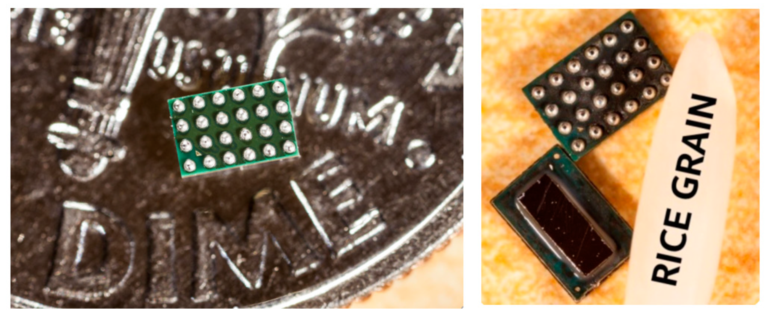
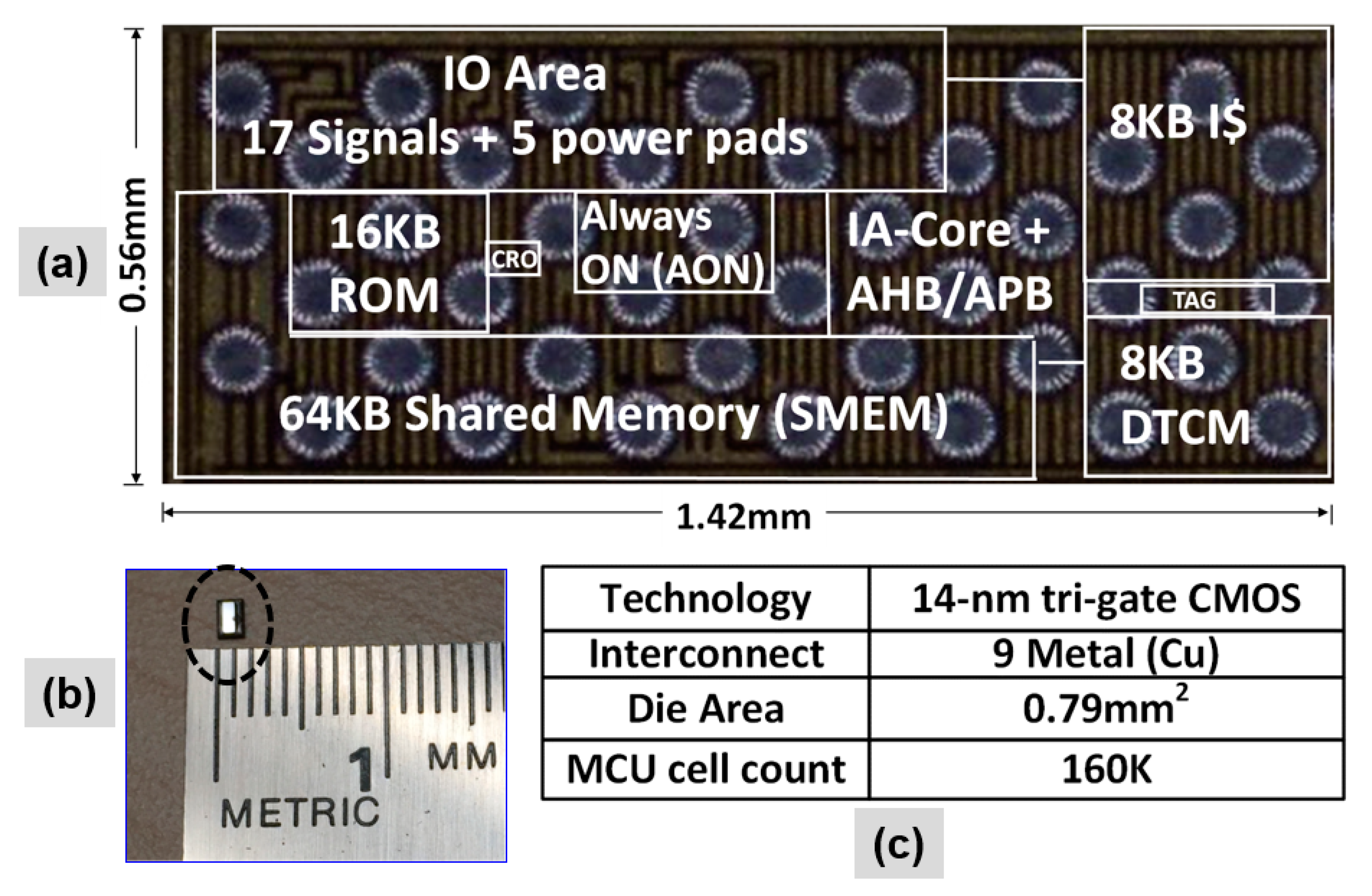
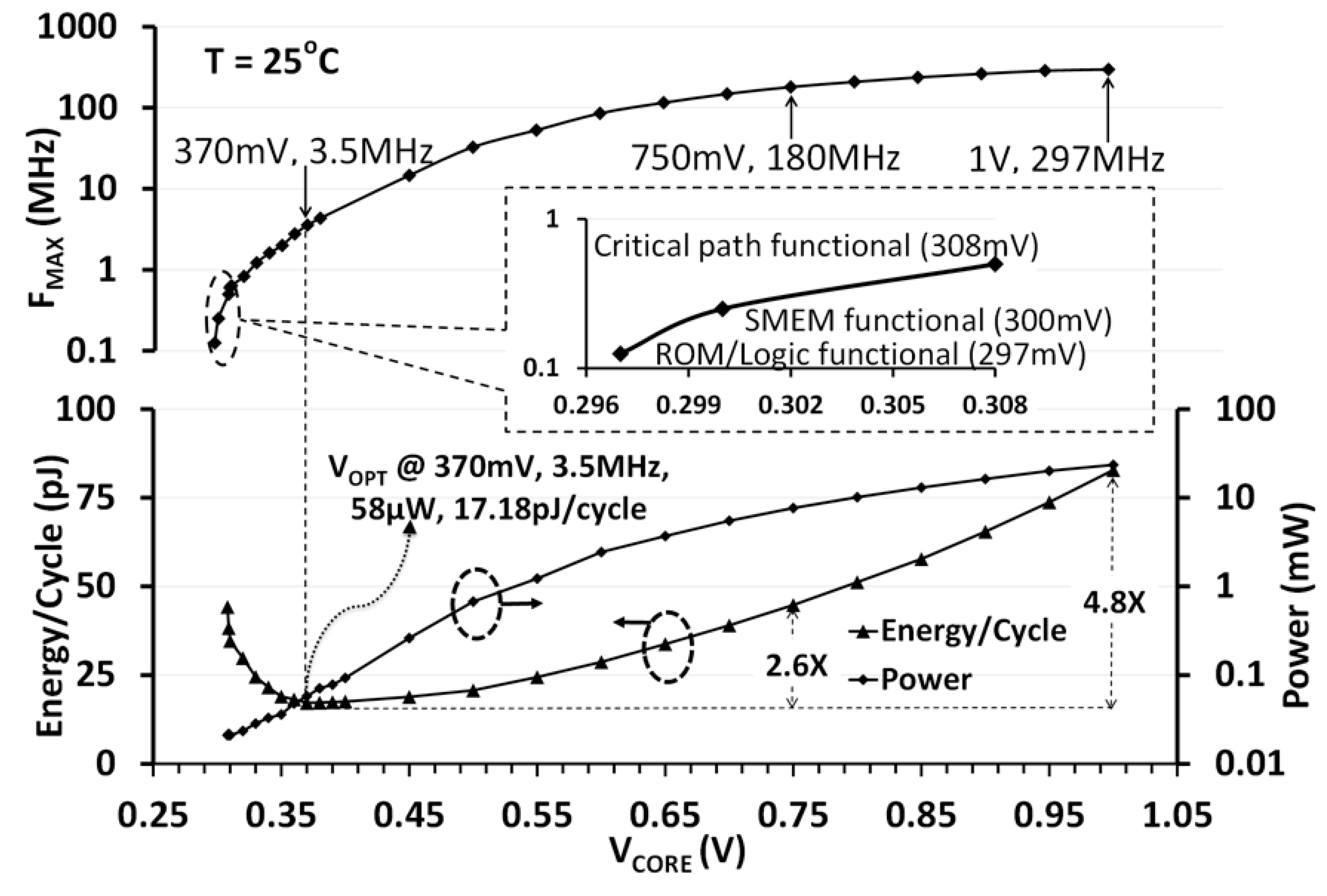
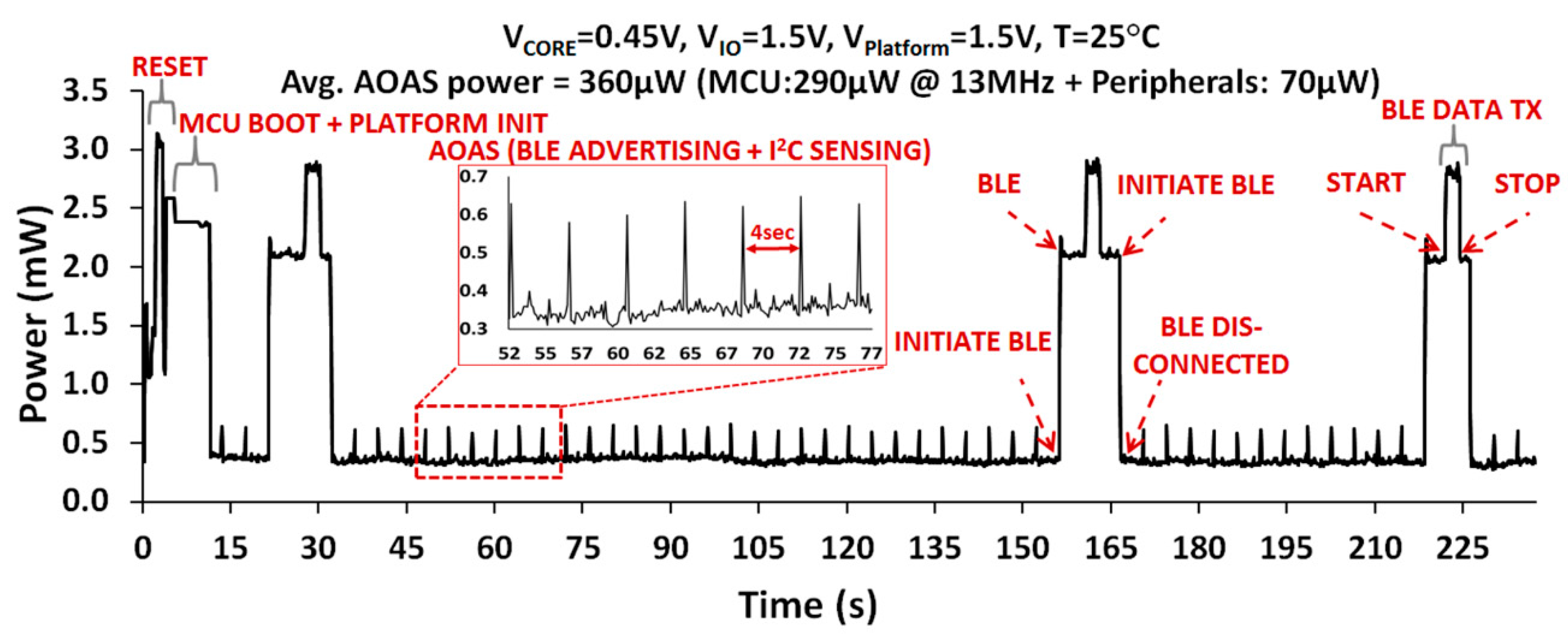
5.4. NTV-MCU Measurement Results and WSN Operation

The MCU is fabricated using 14-nm tri-gate CMOS technology with nine metal interconnect layers (Figure 22). The MCU cell count is approximately 160 K and the die area is 0.79 mm2 (0.56 mm × 1.42 mm). The surface-mount ball grid array (BGA) package has 24 pins with an area of 4.08 mm2 (2.46 mm × 1.66 mm). The die photograph with key IP blocks identified and design characteristics are highlighted in Figure 23. The diminutive low-power MCU can serve as a key component for future autonomous, self-powered “smart dust” WSNs [27]—which can sense, compute, and wirelessly relay real-time information about the ambient.
The IA MCU is functional over a wide operating range (Figure 24) from 297 MHz (1 V) scaling down to 0.5 MHz (308 mV) at 25 °C. While the entire MCU is functional down to 308 mV, SMEM functionality was validated down to 300 mV by independently writing and reading to it via the TAP debug interface. The ROM and the AHB logic are found to be functional down to 297 mV. With the MCU continuously executing a data encryption workload (AES-128), the minimum energy point is observed at 370 mV (VOPT) at T = 25 °C. At VOPT, the MCU operates at 3.5 MHz and dissipates 58 µW power, which translates to an energy-efficiency metric of 17.18 pJ/cycle. Compared to super-threshold operation at 1 V, NTV operation at VOPT achieves 4.8× improvement in energy efficiency.
The MCU integrates 8 KB of Instruction cache (I$) and 8 KB data tightly coupled memory (DTCM). DTCM functions as a local scratch-pad memory, offering low latency (single cycle) and deterministic access, particularly valuable for data-intensive workloads. For typical WSN workloads with code footprint ~16 KB, MCU energy can be further improved by enabling I$ and DTCM. Enabling I$ and DTCM helps to exploit any code and data locality present in the application, thereby reducing the active power consumed in AHB interconnect and large SMEM (64 KB) access. Our experiments show 40% energy improvement is achievable from enabling both I$ and DTCM.
The WSN incorporating the NTV CPU operates continuously using the energy harvested by a 1 cm2 solar cell from indoor light (1000 lux), with sensor data transmitted over BLE radio. The measured WSN power profile in AOAS mode over a 4-min interval is shown in Figure 25. In the AOAS operating mode (with BLE advertising + sensor polling every four seconds), average power (PAVG) for the entire WSN is 360 µW, with the MCU contributing 290 µW (13 MHz, 0.45 V). The MCU power further drops to 120 µW in deep sleep state. In the deep sleep state, the core (IA + AHB) and CRO domains are power gated. The AON logic is still powered-ON and driven by RTC clock.

6. Conclusions and Future Work

NTV computing with wide dynamic operational range offers the flexibility to provide the performance on demand for a variety of workloads while minimizing energy consumption. The technology has the potential to permeate the entire range of computing—from ultra energy-efficient servers, personal and mobile computing to self-powered WSNs. It allows us to exploit the advantages of continued Moore’s law to provide highest energy efficiency for throughput-oriented parallel workloads without compromising performance. The overheads of NTV design techniques in complex SoCs must be carefully balanced against impacts on power-performance at the higher end of the operating regime. Adaptive designs with in-situ monitoring circuitry can help detect and fix timing errors dynamically, but at an added cost. Four case-studies highlighting novel resilient architecture and circuit techniques, multi-voltage designs, and variation-aware design methodologies are presented for realizing robust NTV SoCs in scaled CMOS process nodes. In general, designs can tradeoff performance for reduced leakage power to realize better energy gains at NTV. The results demonstrate 3–9× energy benefits at NTV and the proposed design automation methodology can indeed help achieve greater energy reduction. As a future work project, we intend to build unified reliability models for NTC circuits and systems and validate the model against experimental data obtained across a wide voltage range.

Author Contributions

Conceptualization, S.V., S.P., S.H., A.A., R.K., J.T. and V.D.; methodology, S.V., S.H. and S.P.; software, S.P.; validation, S.V., S.P., A.A. and S.H.; investigation, S.P., A.A. and V.D.; resources, S.V.; data curation, S.P. and S.H.; writing—original draft preparation, S.V.; writing—review and editing, S.V., S.P., S.H., R.K. and V.D.; visualization, S.V.; supervision, S.V., R.K., J.T. and V.D.; project administration, S.V. All authors have read and agreed to the published version of the manuscript.

Funding

This research received no external funding.

Acknowledgments

The authors thank S. Jain, S. Khare, V. Honkote, M. Abbott, T. Majumder, P. Aseron, T. Nguyen, H. Kaul, M. Anders, M. Khellah, S. Mathew at Intel Labs, D. Mallik, and V. Grossnickle at Intel for technical contributions, encouragement, and support and the efforts of Intel’s ATTD team with chip package design and assembly.

Conflicts of Interest

The authors declare no conflict of interest.

References

  1. Ronald, G.; Dreslinski, M.; Wieckowski, D.; Blaauw, D.; Sylvester, D.; Mudge, T. Near-threshold computing: Reclaiming Moore’s law through energy efficient integrated circuits. Proc. IEEE 2010, 98, 253–266. [Google Scholar]
  2. De, V.; Vangal, S.; Krishnamurthy, R. Near Threshold Voltage (NTV) Computing. IEEE Des. Test 2016, 34, 1. [Google Scholar] [CrossRef]
  3. Hanson, S.; Zhai, B.; Bernstein, K.; Blaauw, D.; Bryant, A.; Chang, L.; Das, K.K.; Haensch, W.; Nowak, E.J.; Sylvester, D.M. Ultra low-voltage, minimum energy CMOS. IBM J. Res. Dev. 2006, 50, 469–490. [Google Scholar] [CrossRef] [Green Version]
  4. Jan, C.-H.; Agostinelli, M.; Buehler, M.; Chen, Z.-P.; Choi, S.-J.; Curello, G.; Deshpande, H.; Gannavaram, S.; Hafez, W.; Jalan, U.; et al. A 32nm SoC platform technology with 2nd generation high-k/metal gate transistors optimized for ultra low power, high performance, and high density product applications. IEEE Int. Electron Devices Meet. 2009, 1–4. [Google Scholar] [CrossRef]
  5. Schutz, J. A 3.3V 0.6um BiCMOS Superscalar Microprocessor. In Proceedings of the International Solid State Circuits Conference, Digest of Technical Papers, San Francisco, CA, USA, 16–18 February 1994; pp. 202–203. [Google Scholar]
  6. Jain, S.; Khare, S.; Yada, S.; Ambili, V.; Salihundam, P.; Ramani, S.; Muthukumar, S.; Srinivasan, M.; Kumar, A.; Gb, S.K.; et al. A 280mV-to-1.2V wide-operating-range IA-32 processor in 32nm CMOS. In Proceedings of the 2012 IEEE International Solid-State Circuits Conference, Digest of Technical Papers, San Francisco, CA, USA, 19–23 February 2012; pp. 66–68. [Google Scholar]
  7. Flachs, B.; Asano, S.; Dhong, S.; Hofstee, P.; Gervais, G.; Kim, R.; Le, T.; Liu, P.; Leenstra, J.; Liberty, J.; et al. A streaming processing unit for a CELL processor. In Proceedings of the ISSCC 2005 IEEE International Digest of Technical Papers Solid-State Circuits Conference, San Francisco, CA, USA, 10 February 2005; Volume 1, pp. 134–135. [Google Scholar] [CrossRef]
  8. Hsu, S.; Agarwal, A.; Anders, M.; Mathew, S.; Kaul, H.; Sheikh, F.; Krishnamurthy, R. A 280mV-to-1.1V 256b reconfigurable SIMD vector permutation engine with 2-dimensional shuffle in 22nm CMOS. In Proceedings of the 2012 IEEE International Solid-State Circuits Conference, Institute of Electrical and Electronics Engineers, San Francisco, CA, USA, 19–23 February 2012; pp. 178–180. [Google Scholar]
  9. Jan, C.-H.; Bhattacharya, U.; Brain, R.; Choi, S.-J.; Curello, G.; Gupta, G.; Hafez, W.; Jang, M.; Kang, M.; Komeyli, K.; et al. A 22nm SoC platform technology featuring 3-D tri-gate and high-k/metal gate, optimized for ultra low power, high performance and high density SoC applications. In Proceedings of the 2012 International Electron Devices Meeting, San Francisco, CA, USA, 10–13 December 2012; pp. 311–314. [Google Scholar] [CrossRef]
  10. Paul, S.; Abbott, M.; Kishinevsky, E.; Aseron, P.; Vangal, S.; De, V.; Taylor, G. A 3.6 GB/s 1.3 mW 400 mV 0.051 mm2 near-threshold voltage resilient router in 22-nm tri-gate CMOS. In Proceedings of the VLSI Circuits Symposium Digest of Technical Papers, Kyoto, Japan, 12–14 June 2013; pp. C30–C31. [Google Scholar]
  11. Paul, S.; Honkote, V.; Kim, R.; Majumder, T.; Aseron, P.; Grossnickle, V.; Sankman, R.; Mallik, D.; Jain, S.; Vangal, S.; et al. An energy harvesting wireless sensor node for IoT systems featuring a near-threshold voltage IA-32 microcontroller in 14nm tri-gate CMOS. In Proceedings of the 2016 IEEE Symposium on VLSI Circuits (VLSI-Circuits), Honolulu, HI, USA, 15–17 June 2016; pp. 1–2. [Google Scholar] [CrossRef]
  12. Vangal, S.R.; Howard, J.; Ruhl, G.; Dighe, S.; Wilson, H.; Tschanz, J.; Finan, D.; Singh, A.P.; Jacob, T.; Jain, S.; et al. An 80-Tile Sub-100-W TeraFLOPS Processor in 65-nm CMOS. IEEE J. Solid-State Circuits 2008, 43, 29–41. [Google Scholar] [CrossRef]
  13. Vangal, S.; Singh, A.P.; Howard, J.; Dighe, S.; Borkar, N.; Alvandpour, A. A 5.1GHz 0.34mm2 Router for Network-on-Chip Applications. In Proceedings of the 2007 IEEE Symposium on VLSI Circuits, Kyoto, Japan, 14–16 June 2007; pp. 42–43. [Google Scholar] [CrossRef]
  14. Jan, C.H.; Al-Amoody, F.; Chang, H.Y.; Chang, T.; Chen, Y.W.; Dias, N.; Hafez, W.; Ingerly, D.; Jang, M.; Karl, E.; et al. A 14 nm SoC platform technology featuring 2nd generation tri-gate transistors, 70 nm gate pitch, 52 nm metal pitch, and 0.0499 µm2 SRAM cells, optimized for low power, high performance and high density SoC products. In Proceedings of the 2015 Symposium on VLSI Technology (VLSI Technology), Kyoto, Japan, 16–18 June 2015. [Google Scholar]
  15. Intel Corporation. Intel Quark Processors. Available online: http://www.intel.com/content/www/us/en/embedded/products/quark/overview.html (accessed on 1 April 2020).
  16. Raychowdhury, A.; Geuskens, B.; Kulkarni, J.P.; Tschanz, J.; Bowman, K.; Karnik, T.; Lu, S.-L.; De, V.; Khellah, M.M. PVT-and-aging adaptive wordline boosting for 8T SRAM power reduction. In Proceedings of the 2010 IEEE International Solid-State Circuits Conference (ISSCC), San Francisco, CA, USA, 7–11 February 2010; pp. 352–353. [Google Scholar] [CrossRef]
  17. Kulkarni, J.P.; Geuskens, B.; Karnik, T.; Khellah, M.; Tschanz, J.; De, V. Capacitive-coupling wordline boosting with self-induced VCC collapse for write VMIN reduction in 22-nm 8T SRAM. In Proceedings of the 2012 IEEE International Solid-State Circuits Conference, San Francisco, CA, USA, 19–23 February 2012; pp. 234–236. [Google Scholar] [CrossRef]
  18. Pinckney, N.; Sewell, K.; Dreslinski, R.G.; Fick, D.; Mudge, T.; Sylvester, D.; Blaauw, D. Assessing the performance limits of parallelized near-threshold computing. In Proceedings of the 49th Annual Design Automation Conference, Association for Computing Machinery (ACM), San Francisco, CA, USA, 3–7 June 2012; p. 1147. [Google Scholar]
  19. Tschanz, J.; Lam, C.; Shuman, M.; Tokunaga, C.; Somasekhar, D.; Tang, S.; Finan, D.; Karnik, T.; Borkar, N.; Kurd, N.; et al. Adaptive Frequency and Biasing Techniques for Tolerance to Dynamic Temperature-Voltage Variations and Aging. In Proceedings of the 2007 IEEE International Solid-State Circuits Conference Digest of Technical Papers, San Francisco, CA, USA, 11–15 February 2007; pp. 292–604. [Google Scholar]
  20. Tschanz, J.; Bowman, K.; Walstra, S.; Agostinelli, M.; Karnik, T.; De, V. Tunable replica circuits and adaptive voltage-frequency techniques for dynamic voltage, temperature, and aging variation tolerance. In Proceedings of the 2009 Symposium on VLSI Circuits, Digest of Technical Papers, Kyoto, Japan, 16–18 June 2009; pp. 112–113. [Google Scholar]
  21. Bowman, K.A.; Tschanz, J.W.; Kim, N.S.; Lee, J.C.; Wilkerson, C.B.; Lu, S.-L.L.; Karnik, T.; De, V. Energy-Efficient and Metastability-Immune Resilient Circuits for Dynamic Variation Tolerance. IEEE J. Solid-State Circuits 2008, 44, 49–63. [Google Scholar] [CrossRef]
  22. Rossi, D.; Metra, C.; Nieuwland, A.K.; Katoch, A. New ECC for crosstalk effect minimization. IEEE Des. Test Comput. 2005, 22, 340–348. [Google Scholar] [CrossRef]
  23. Amin, C.S.; Menezes, N.; Killpack, K.; Dartu, F.; Choudhury, U.; Hakim, N.; Ismail, Y.I. Statistical static timing analysis. In Proceedings of the 42nd Design Automation Conference, Association for Computing Machinery (ACM), Anaheim, CA, USA, 13–17 June 2005; p. 652. [Google Scholar]
  24. Singhee, A.; Singhal, S.; Rutenbar, R.A. Practical, fast Monte Carlo statistical static timing analysis: Why and how. In Proceedings of the 2008 IEEE/ACM International Conference on Computer-Aided Design, San Jose, CA, USA, 10–13 November 2008; pp. 190–195. [Google Scholar]
  25. Cho, M.; Khellah, M.; Chae, K.; Ahmed, K.; Tschanz, J.; Mukhopadhyay, S. Characterization of Inverse Temperature Dependence in logic circuits. In Proceedings of the IEEE 2012 Custom Integrated Circuits Conference, San Jose, CA, USA, 9–12 September 2012; pp. 1–4. [Google Scholar]
  26. Han, S.; Guo, D.; Wang, X.; Mocuta, A.C.; Henson, W.K.; Rim, K. Reverse Temperature Dependence of Circuit Performance in High-k/Metal-Gate Technology. IEEE Electron Device Lett. 2009, 30, 1344–1346. [Google Scholar]
  27. Warneke, B.; Last, M.; Liebowitz, B.; Pister, K. Smart Dust: Communicating with a cubic-millimeter computer. Computer 2001, 34, 44–51. [Google Scholar] [CrossRef]
Figure 1. Block diagrams for four NTV prototypes: (a) Pentium™ class IA-32 CPU; (b) Reconfigurable 256-bit wide SIMD vector permutation engine with 2-D Shuffle; (c) Resilient four node (2 × 2) 2-D Mesh NoC fabric with routers (R1–R4); (d) mm-scale MCU with NTV Quark IA-32 core for µW WSNs.
Jlpea 10 00016 g001
Figure 2. The prototypes use variability-tolerant SRAM bit-cells: (a) 8-T SRAM bit-cell used in the NTV-MCU; (b) The SIMD engine uses a 10-T dual-ended transmission gate (DETG) SRAM topology; (c) An alternate 10-T transmission gate (TG) SRAM bit-cell used in the NTV-CPU; (d) Simulated retention voltage simulations for the 10-T TG SRAM in 32-nm, as a function of keeper device size (m9, m10) in the presence of random variations (5.9σ, slow skew, −25 °C); (e) The shared PMOS/NMOS on the virtual supplies improve memory write Vmin by 125 mV in the 22-nm DETG based memory array.
Jlpea 10 00016 g002
Figure 3. Simulated 32-nm normalized gate delays (y-axis) vs. supply voltage for logic devices in the presence of random variations (6σ). To limit excessive gate delays at NTV, the data indicates that: (a) Transistor stack sizes need to be limited to three, including; (b) Wide pass-gate multiplexers; (c) High VT devices have 76% higher delay penalty over nominal VT flavors due to variations; and (d) Minimum width (1×, ZMIN) devices show 130% higher delay at 500 mV, requiring restricted use.
Jlpea 10 00016 g003
Figure 4. Low-voltage pass-gate free sequential circuit: (a) clocked-CMOS-style flip-flop implementation; (b) Clocked inverter logic gate.
Jlpea 10 00016 g004
Figure 5. Averaging impact of device parameter variations at NTV: (a) vector flip-flop topology with shared clock input drivers; (b) Simulated hold time improvement in 22-nm node in the presence of random variations (6σ).
Jlpea 10 00016 g005
Figure 6. Ultra-low voltage split-output (ULVS) level shifter: (a) Circuit diagram with critical devices circled; (b) Simulated 22-nm Vmin benefit of 125mV node in the presence of random variations (6σ).
Jlpea 10 00016 g006
Figure 7. Simulated 22nm SIMD engine register file and logic optimization benefits across 0–85 °C, 3σ systematic, 6σ random variation.
Jlpea 10 00016 g007
Figure 8. NTV-NoC: (a) Two-stage router data path and control logic indicating critical timing path; (b) Pipe stage 2 is enhanced with EDS circuit to detect failures in critical timing paths down to NTV.
Jlpea 10 00016 g008
Figure 9. Internal router architecture: (a) Modifications to enable FLIT replay and forward error correction; (b) Clock cycle diagram showing stages of timing failure detection, replay and recovery.
Jlpea 10 00016 g009
Figure 10. NTV-CPU: (a) Optimizations for wide range design convergence; (b) Design criteria varies widely at NTV (0.5 V) vs.1.05 V corner.
Jlpea 10 00016 g010
Figure 11. Multi-voltage global clock generation and distribution: (a) Calibrated Ring Oscillator (CRO) used in 14-nm NTV-MCU; (b) CRO operating range in both open/closed loops with µW power consumption; (c) The global clock distribution in the 32-nm NTV-CPU uses multi-stage level shifters; (d) Simulated clock skew reduction benefit from voltage specific delay tuning using look-up tables.
Jlpea 10 00016 g011
Figure 12. NTV-CPU: (a) Full-Chip 32-nm die and core micrographs and characteristics; (b) Packaged IA-32 silicon and the small solar cell used to power the core.
Jlpea 10 00016 g012
Figure 13. NTV-CPU measured power, performance and energy characteristics across wide VDD.
Jlpea 10 00016 g013
Figure 14. Measured NTV-CPU power breakdown across wide voltage range. Note that the memory supply scales down to 550mV, while the core logic operates well into the sub-threshold regime.
Jlpea 10 00016 g014
Figure 15. NTV-SIMD vector engine die micrographs and characteristics.
Jlpea 10 00016 g015
Figure 16. Measured NTV-SIMD engine: (a) Maximum frequency and power vs. VDD (b) Energy efficiency vs. VDD.
Jlpea 10 00016 g016
Figure 17. NTV-NoC design: (a) Die photograph with supply noise injectors; (b) Experiment setup; (c) NoC layout with key IP blocks identified and 1.5 mm folded links (d) Die characteristics.
Jlpea 10 00016 g017
Figure 18. Measured 2 × 2 NoC power, performance and energy characteristics across wide voltage range with EDS and replay mechanisms disabled.
Jlpea 10 00016 g018
Figure 19. Silicon logic analyzer trace showing successful recovery of FLITs from timing failures.
Jlpea 10 00016 g019
Figure 20. Improvement in resilient router bandwidth at VOPT (400 mV) over a non-resilient version.
Jlpea 10 00016 g020
Figure 21. Measured NTV-NoC resilience to temperature variations and ITD effects at 400 mV. Timing failures in a conventional router increases at a faster rate over an EDS-enhanced one. The percentage of failing FLITS is indicated in the secondary y-axis.
Jlpea 10 00016 g021
Figure 22. The 32-b IA NTV MCU is packaged in a miniature 4.08-mm2 (2.46 mm × 1.63 mm) 24-pin BGA substrate.
Jlpea 10 00016 g022
Figure 23. NTV-MCU 14-nm design: (a) Die photograph with key IP blocks identified. The die area is dominated by 64 KB of shared memory (SMEM); (b) Packaged 4 mm2 die; (c) Die characteristics.
Jlpea 10 00016 g023
Figure 24. Measured 14-nm NTV-MCU power, performance, and energy efficiency across wide VDD.
Jlpea 10 00016 g024
Figure 25. Measured WSN power profile in AOAS mode over a 4-min interval.
Jlpea 10 00016 g025
Table 1. A summary of four NTV-optimized silicon designs from Intel Labs.
ISSCC 2012 [6]ISSCC 2012 [8]VLSI 2013 [10]VLSI 2016 [11]
NTV Design32-b ×86 CPU SIMD Engine2D NoC fabric mm-scale MCU
Intel CMOS Technology32-nm high-K/metal-gate 22-nm Tri-gate 22-nm Tri-gate14nm Tri-gate
Die Area (mm2)20.048Router: 0.051
2 × 2 Mesh: 0.93
0.79
VDD range and VOPT (V)0.28–1.2
(VOPT = 0.45)
0.24–1.1
(VOPT = 0.26)
0.34–0.85
(VOPT = 0.4)
0.308–1.0
(VOPT = 0.37)
Frequency range (MHz)3–91510–29000.5–29767–1000
Energy @ VOPT Benefit170pJ/cyclea, 4.7×1.9pJ/cycle,
36pJ/cycleb,
3.3×
17.18pJ/cyclec,
4.8×
Total on-chip memory8KB I$ + 8KB D$1KB Reg. file (RF) memoryNone8KB I$ + 8KB DTCM + 64KB SMEM + 16KB BootROM
a Pentium BIST workload, b For 2 × 2 NoC, c MCU always-active, running AES encryption.
Table 2. Comparison between 8T SRAMS build with ULP and SP bit-cells.
8T SRAM Device Type.Gate PitchNormalized Frequency (0.5V)Normalized Leakage
(0.5V, 25C)
14 nm Bit-Cell Area (µm2)
Standard performance (SP)70nm26×0.100 µm2
Ultralow power (ULP, NTV MCU Memory)84nm0.155 µm2 (1.55×)

